

General Description
The MAX8731 is an SMBus™ programmable multichemistry battery charger. The MAX8731 uses a minimal
command set to easily program the charge voltage,
charge current, and adapter current limit.
The MAX8731 charges one to four Li+ series cells and
delivers up to 8A charge current. The MAX8731 drives
n-channel MOSFETs for improved efficiency and
reduced cost. Low-offset current-sense amplifiers provide high accuracy with 10mΩ sense resistors.
The MAX8731 current-sense amplifiers provide high
accuracy (3% at 3.5A) and also provide fast cycle-bycycle current-mode control to protect against battery
short circuit and system load transients.
The charger employs dual remote-sense, which reduces
charge time by measuring the feedback voltage directly
at the battery, improving accuracy of initial transition into
constant-voltage mode. The MAX8731 provides 0.5%
battery voltage accuracy directly at the battery terminal.
The MAX8731 provides a digital output that indicates the
presence of the AC adapter, as well as an analog output
that indicates the adapter current within 4% accuracy.
The MAX8731 is available in a small 5mm x 5mm,
28-pin, thin (0.8mm) QFN package. An evaluation kit is
available to reduce design time. The MAX8731 is available in lead-free packages.
Applications
Notebook Computers
Tablet PCs
Medical Devices
Portable Equipment with Rechargeable Batteries
Features
♦ 0.5% Battery Voltage Accuracy
♦ 3% Input Current-Limit Accuracy
♦ 3% Charge-Current Accuracy
♦ SMBus 2-Wire Serial Interface
♦ Cycle-by-Cycle Current Limit
Battery Short-Circuit Protection
Fast Response for Pulse Charging
Fast System-Load-Transient Response
♦ Dual-Remote-Sense Inputs
♦ Monitor Outputs for
Adapter Current (4% Accuracy)
AC Adapter Detection
♦ 11-Bit Battery Voltage Setting
♦ 6-Bit Charge-Current/Input-Current Setting
♦ 8A (max) Battery Charger Current
♦ 11A (max) Input Current
♦ +8V to +26V Input Voltage Range
♦ Charges Li+, NiMH, and NiCd Battery Chemistries
MAX8731
SMBus Level 2 Battery Charger with
Remote Sense
________________________________________________________________ Maxim Integrated Products 1
Ordering Information
Typical Operating Circuit
19-3923; Rev 0; 1/06
For pricing, delivery, and ordering information, please contact Maxim/Dallas Direct! at
1-888-629-4642, or visit Maxim’s website at www.maxim-ic.com.
SMBus is a trademark of Intel Corp.
+Indicates lead-free packaging.
EVALUATION KIT
AVAILABLE
Pin Configuration
TOP VIEW
DCIN
DHI
BST
V
CSSN
CSSP
22
LX
23
24
25
26
CC
27
28
12
PGND
DLO
CSIP
LDO
2021 19 17 16 15
*EXPOSED PADDLE
GND
ACIN
THIN QFN
5mm x 5mm
CSIN
18
MAX8731
4567
3
CCI
REF
CCS
FBSB
CCV
FBSA
DAC
14
BATSEL
ACOK
13
12
GND
V
11
DD
10
SCL
SDA
9
8
IINP
PART TEMP RANGE PIN-PACKAGE
MAX8731ETI+ -40°C to +85°C 28 Thin QFN (5mm x 5mm)
OPTIONAL
HOST
SCL
SDA
VDD
CSSP CSSN
ACIN
DCIN
ACOK
REF
GND
BATSEL
SCL
SDA
V
DD
GND
IINP CCV
DAC
MAX8731
CCS
DHI
DLO
PGND
BST
CSIP
CSIN
FBSA
FBSB
LDO
V
CCI
LX
CC
N
N
EXTERNAL
LOAD
SELECTOR
BATSEL
BATTERY
A
BATTERY
B
SMBus Level 2 Battery Charger with
Remote Sense
2 _______________________________________________________________________________________
ABSOLUTE MAXIMUM RATINGS
ELECTRICAL CHARACTERISTICS
(V
DCIN
= VLX= V
CSSP
= V
CSSN
= 19V, V
BST
- VLX= 4.5V, V
FBSA
= V
FBSB
= V
CSIP
= V
CSIN
= 16.8V, BATSEL = GND = PGND = 0,
C
LDO
= 1µF, VCC= LDO, C
REF
= 1µF, C
DAC
= 0.1µF, VDD= 3.3V, ACIN = 2.5V; pins CCI, CCV, and CCS are compensated per
Figure 1; T
A
= 0°C to +85°C, unless otherwise noted. Typical values are at TA= +25°C.)
Stresses beyond those listed under “Absolute Maximum Ratings” may cause permanent damage to the device. These are stress ratings only, and functional
operation of the device at these or any other conditions beyond those indicated in the operational sections of the specifications is not implied. Exposure to
absolute maximum rating conditions for extended periods may affect device reliability.
DCIN, CSSN, CSIN, FBSA, FBSB to GND..............-0.3V to +28V
CSSP to CSSN, CSIP to CSIN, PGND to GND ......-0.3V to +0.3V
BST to GND ............................................................-0.3V to +32V
BST to LX..................................................................-0.3V to +6V
DHI to LX.................................................-0.3V to +(V
BST
+ 0.3)V
DLO to PGND..........................................-0.3V to +(LDO + 0.3)V
LX to GND .................................................................-6V to +28V
CCI, CCS, CCV, DAC, REF,
IINP to GND...........................................-0.3V to (V
VCC
+ 0.3)V
V
DD
, SCL, SDA, BATSEL, ACIN, ACOK, VCCto GND,
LDO to PGND ......................................................-0.3V to +6V
Continuous Power Dissipation (T
A
= +70°C)
28-Pin Thin QFN
(derate 20.8mW/°C above +70°C)........................1666.7 mW
Operating Temperature Range ...........................-40°C to +85°C
Junction Temperature......................................................+150°C
Storage Temperature Range .............................-60°C to +150°C
Lead Temperature (soldering, 10s) .................................+300°C
MAX8731
PARAMETER CONDITIONS MIN TYP MAX UNITS
CHARGE-VOLTAGE REGULATION
ChargingVoltage() = 0x41A0
ChargingVoltage() = 0x3130
Battery Full-Charge Voltage and
Accuracy
ChargingVoltage() = 0x20D0
ChargingVoltage() = 0x1060
Battery Undervoltage-Lockout
Trip Point for Trickle Charge
2.5 V
CHARGE-CURRENT REGULATION
CSIP to CSIN Full-Scale Current-
Sense Voltage
78.22 80.64 83.06 mV
RS2 (Figure 1) = 10mΩ;
ChargingCurrent() = 0x1f80
Charge Current and Accuracy
RS2 (Figure 1) = 10mΩ;
ChargingCurrent() = 0x0f80
RS2 (Figure 1) = 10mΩ;
ChargingCurrent() = 0x0080 (128mA)
Charge-Current Gain Error Based on ChargeCurrent() = 128mA and 8.064A -2 +2 %
FBSA/FBSB/CSIP/CSIN
Input Voltage Range
0 19 V
16.716 16.8 16.884 V
-0.5 +0.5 %
12.491 12.592 12.693 V
-0.8 +0.8 %
8.333 8.4 8.467 V
-0.8 +0.8 %
4.15 4.192 4.234 V
-1.0 +1.0 %
7.822 8.064 8.306 A
-3 +3 %
3.809 3.968 4.126 A
-4 +4 %
64 400 mA
MAX8731
SMBus Level 2 Battery Charger with
Remote Sense
_______________________________________________________________________________________ 3
ELECTRICAL CHARACTERISTICS (continued)
(V
DCIN
= VLX= V
CSSP
= V
CSSN
= 19V, V
BST
- VLX= 4.5V, V
FBSA
= V
FBSB
= V
CSIP
= V
CSIN
= 16.8V, BATSEL = GND = PGND = 0,
C
LDO
= 1µF, VCC= LDO, C
REF
= 1µF, C
DAC
= 0.1µF, VDD= 3.3V, ACIN = 2.5V; pins CCI, CCV, and CCS are compensated per
Figure 1; T
A
= 0°C to +85°C, unless otherwise noted. Typical values are at TA= +25°C.)
PARAMETER CONDITIONS MIN TYP MAX UNITS
Battery Quiescent Current
Adapter Quiescent Current
INPUT-CURRENT REGULATION
CSSP to CSSN Full-Scale
Current-Sense Voltage
Input Current Accuracy
POR Input Current RS1 (Figure 1) = 10mΩ 256 mA
Input Current-Limit Gain Error -2 +2 %
Input Current-Limit Offset
CSSP/CSSN Input Voltage Range 8 26 V
IINP Transconductance V
IINP Offset Based on V
IINP Accuracy
IINP Output Voltage Range 0 3.5 V
SUPPLY AND LINEAR REGULATOR
DCIN, Input Voltage Range 8.0 26.0 V
DCIN Undervoltage-Lockout
Trip Point
Power-Fail Threshold
Adapter present, not charging, I
V
Ad ap ter ab sent, I
+ I
I
DCIN
I
CSSP
I
CSSN
V
RS1 (Figure 1) = 10mΩ, InputCurrent() = 11004mA or
3584mA
= VLX = V
FBS_
, V
C S S N
FBS _
+
+
= 19V 106.7 110 113.3 mV
FBS_
CSIN
C S I P
= V
LX
V
Adapter
charging
V
Adapter
V
Battery
V
Adapter
V
Battery
= V
+ I
= V
= 26V, V
= 19V,
= 16.8V
= 8V,
= 4V
CSIP
C S I N
C S I N
= 19V
+ I
= V
Battery
LX
CSIP
+ I
C S I P
+ I
CSIN
FBS A
= 19V , V
= 16.8V, not
+ I
FBS B
+ ILX + I
+ I
= 0V
D C I N
FBS,
C S S P
2 5
+1
200 500 µA
Charging 0.4 1 mA
Not charging 200 500 µA
Charging 0.4 1 mA
Not charging 200 500 µA
-3 +3 %
RS1 (Figure 1) = 10mΩ, InputCurrent() = 2048mA -5 +5 %
Based on InputCurrent() = 1024mA and 11004mA
CSSP - CSSN
V
CSSP - CSSN
V
CSSP - CSSN
V
CSSP - CSSN
= 110mV 2.85 3.0 3.15 mA/V
CSSP - CSSN
= 110mV -5 +5
= 55mV or 35mV -4 +4
= 20mV -10 +10
= 110mV and 20mV -1.5 +1.5 mV
-1 +1 mV
DCIN falling 7 7.4
DCIN rising 7.5 7.85
V
- V
CSSP
V
CSSP
falling 9 15 21
CSIN
- V
rising 160 210 271
CSIN
µA
%
V
mV
MAX8731
SMBus Level 2 Battery Charger with
Remote Sense
4 _______________________________________________________________________________________
ELECTRICAL CHARACTERISTICS (continued)
(V
DCIN
= VLX= V
CSSP
= V
CSSN
= 19V, V
BST
- VLX= 4.5V, V
FBSA
= V
FBSB
= V
CSIP
= V
CSIN
= 16.8V, BATSEL = GND = PGND = 0,
C
LDO
= 1µF, VCC= LDO, C
REF
= 1µF, C
DAC
= 0.1µF, VDD= 3.3V, ACIN = 2.5V; pins CCI, CCV, and CCS are compensated per
Figure 1; T
A
= 0°C to +85°C, unless otherwise noted. Typical values are at TA= +25°C.)
PARAMETER CONDITIONS MIN TYP MAX UNITS
LDO Output Voltage 8.0V < V
LDO Load Regulation 0 < I
LDO Undervoltage-Lockout Threshold V
V
Range 2.7 5.5 V
DD
V
UVLO Rising 2.5 2.7 V
DD
V
UVLO Hysteresis 100 mV
DD
V
Quiescent Current DCIN < 6V, VDD = 5.5V, SCL = SDA = 5.5V 16 27 µA
DD
REFERENCE
REF Output Voltage 0 < I
REF Undervoltage-Lockout Trip Point REF falling 3.1 3.9 V
ACOK
ACOK Sink Current V
ACOK Leakage Current V
ACIN
ACIN Threshold 2.007 2.048 2.089 V
ACIN Threshold Hysteresis 10 20 30 mV
ACIN Input Bias Current -1 +1 µA
REMOTE-SENSE INPUTS
FBS_ Range V
FBS_ Gain ∆V
CSIN-FBS_ Clamp Voltage 225 250 275 mV
FBS_ Bias Current Charger switching, FBS_ selected 14 µA
FBS_ Bias Current Charger not switching or FBS_ not selected -2 +2 µA
SWITCHING REGULATOR
Off-Time
BST Supply Current DHI high 500 800 µA
LX Input Bias Current V
Maximum Discontinuous-Mode Peak
Current (I
MIN
)
DHI On-Resistance Low I
DHI On-Resistance High I
DLO On-Resistance High I
DLO On-Resistance Low I
< 28V, no load 5.25 5.4 5.55 V
DCIN
< 30mA 34 100 mV
LDO
= 8.0V, V
DCIN
REF
= 0.4V, ACIN = 1.5V 1 mA
ACOK
= 5.5V, ACIN = 2.5V 1 µA
ACOK
- V
CSIN
/ ∆(V
CSIN
V
= 16.0V, V
CSIN
V
= 16.0V, V
CSIN
= 28V, V
DCIN
LDO
< 500µA 4.071 4.096 4.120 V
FBS
CSIN
CSIN
falling 3.20 4 5.15 V
0 200 mV
- V
) 0.95 1.00 1.05 V/V
FBS_
= 19V 360 400 440
CSSP
= 17V 260 300 360
CSSP
= VLX
= 20V, DHI low
2 µA
0.5 A
= -10mA 1 3 Ω
DHI
= 10mA 3 5 Ω
DHI
= 10mA 3 5 Ω
DLO
= -10mA 1 3 Ω
DLO
ns
ELECTRICAL CHARACTERISTICS (continued)
(V
DCIN
= VLX= V
CSSP
= V
CSSN
= 19V, V
BST
- VLX= 4.5V, V
FBSA
= V
FBSB
= V
CSIP
= V
CSIN
= 16.8V, BATSEL = GND = PGND = 0,
C
LDO
= 1µF, VCC= LDO, C
REF
= 1µF, C
DAC
= 0.1µF, VDD= 3.3V, ACIN = 2.5V; pins CCI, CCV, and CCS are compensated per
Figure 1; T
A
= 0°C to +85°C, unless otherwise noted. Typical values are at TA= +25°C.)
MAX8731
SMBus Level 2 Battery Charger with
Remote Sense
_______________________________________________________________________________________ 5
ERROR AMPLIFIERS
GMV Amplifier Transconductance C har g i ng V ol tag e( ) = 16.8V , V
GMI Amplifier Transconductance ChargingCurrent() = 3968mA, V
GMS Amplifier Transconductance InputCurrent() = 3968mA, V
CCI/CCS/CCV Clamp Voltage
LOGIC LEVELS
SDA/SCL Input Low Voltage VDD = 2.7V to 5.5V 0.8
SDA/SCL Input High Voltage VDD = 2.7V to 5.5V 2.1
SDA/SCL Input Bias Current VDD = 2.7V to 5.5V -1 +1
BATSEL Input Low Voltage 0.8
BATSEL Input High Voltage 2.1
BATSEL Input Bias Current -1 +1
SDA, Output Sink Current V
SMBus TIMING SPECIFICATIONS (VDD = 2.7V to 5.5V) (see Figures 4 and 5)
SMBus Frequency f
Bus Free Time t
Start Condition Hold Time from
SCL
Start Condition Setup Time from
SCL
Stop Condition Setup Time from
SCL
SDA Hold Time from SCL t
SDA Setup Time from SCL t
SCL Low Timeout t
SCL Low Period T
SCL High Period T
Maximum Charging Period
Without a ChargeVoltage() or
ChargeCurrent() Command
PARAMETER CONDITIONS
PARAMETERS SYMBOL CONDITIONS MIN TYP MAX UNITS
0.25V < V
(SDA)
t
t
t
TIMEOUT
< 2.0V
CCI/S/V
= 0.4V 6
SMB
BUF
HD:STA
SU:STA
SU:STO
HD:DAT
SU:DAT
(Note 1) 25 35
LOW
HIGH
FBS_
CSSP
= 16.8V
- V
CSIP
- V
CSSN
= 39.68mV
CSIN
= 79.36mV
MIN TYP MAX UNITS
0.0625 0.125 0.2500 mA/V
0.5
0.5
120
10 100
4.7
4
4.7
4
300
250
4.7
4
140 175 210
1
1
250
2.0
2.0
600
mA/V
mA/V
mV
V
V
µA
V
V
µA
mA
kHz
µs
µs
µs
µs
ns
ns
ms
µs
µs
s
MAX8731
SMBus Level 2 Battery Charger with
Remote Sense
6 _______________________________________________________________________________________
ELECTRICAL CHARACTERISTICS
(V
DCIN
= VLX= V
CSSP
= V
CSSN
= 19V, V
BST
- V
LX
= 4.5V, V
FBSA
= V
FBSB
= V
CSIP
= V
CSIN
= 16.8V, BATSEL = GND = PGND = 0,
C
LDO
= 1µF, VCC= LDO, C
REF
= 1µF, C
DAC
= 0.1µF , VDD= 3.3V, ACIN = 2.5V; pins CCI, CCV, and CCS are compensated per
Figure 1; T
A
= -40°C to +85°C, unless otherwise noted.) (Note 2)
PARAMETER CONDITIONS
MIN
TYP
MAX
UNITS
CHARGE-VOLTAGE REGULATION
V
ChargingVoltage() = 0x41A0
-1 +1 %
V
ChargingVoltage() = 0x3130
-1 +1 %
V
ChargingVoltage() = 0x20D0
-1 +1 %
V
Battery Full-Charge Voltage and
Accuracy
ChargingVoltage() = 0x1060
%
CHARGE-CURRENT REGULATION
CSIP to CSIN Full-Scale Current-
Sense Voltage
mV
A
RS2 (Figure 1) = 10mΩ;
ChargingCurrent()= 0x1f80
-3 +3 %
A
RS2 (Figure 1) = 10mΩ;
ChargingCurrent() = 0x0f80
-4 +4 %
Charge Current and Accuracy
RS2 (Figure 1) =10mΩ;
ChargingCurrent() = 0x0080
30
mA
Charge-Current Gain Error Based on ChargeCurrent() = 128mA and 8.064A -2 +2 %
FBSA/FBSB/CSIP/CSIN Input
Voltage Range
0 19 V
Adapter present, not charging, I
CSIP
+ I
CSIN
+ ILX + I
FBS
,
V
FBS_
= VLX = V
CSIN
= V
CSIP
= 19V
5
Battery Quiescent Current
Adapter absent, I
CSIP
+ I
CSIN
+ ILX + I
FBSA
+ I
FBSB
+
I
CSSP
+ I
CSSN
, V
FBS_
= VLX = V
CSIN
= V
CSIP
= 19V,
V
DCIN
= 0V
1
µA
µA
Charging 1 mA
V
Adapter
= 19V,
V
Battery
= 16.8V
Not charging
µA
Charging 1 mA
Adapter Quiescent Current
I
DCIN
+
I
CSSP
+
I
CSSN
V
Adapter
= 8V,
V
Battery
= 4V
Not charging
µA
16.632
12.466
8.316
4.129
-1.5
78.22
7.822
3.809
V
A d a p t er
= 26V , V
= 16.8V , not char g i ng
B at te r y
16.968
12.717
8.484
4.255
+1.5
83.05
8.305
4.126
400
500
500
500
MAX8731
SMBus Level 2 Battery Charger with
Remote Sense
_______________________________________________________________________________________ 7
ELECTRICAL CHARACTERISTICS (continued)
(V
DCIN
= VLX= V
CSSP
= V
CSSN
= 19V, V
BST
- V
LX
= 4.5V, V
FBSA
= V
FBSB
= V
CSIP
= V
CSIN
= 16.8V, BATSEL = GND = PGND = 0,
C
LDO
= 1µF, VCC= LDO, C
REF
= 1µF, C
DAC
= 0.1µF , VDD= 3.3V, ACIN = 2.5V; pins CCI, CCV, and CCS are compensated per
Figure 1; T
A
= -40°C to +85°C, unless otherwise noted.) (Note 2)
PARAMETER CONDITIONS
UNITS
INPUT-CURRENT REGULATION
CSSP to CSSN Full-Scale
Current-Sense Voltage
V
FBS_
= 19V
mV
RS1 (Figure 1) = 10mΩ;
InputCurrent() = 11004mA or 3584mA
-6 +6
Input Current Accuracy
RS1 (Figure 1) = 10mΩ;
InputCurrent() = 2048mA
-5 +5
%
Input Current-Limit Gain Error Based on InputCurrent() = 1024mA and 11004mA -5 +5 %
Input Current-Limit Offset Based on InputCurrent() = 1024mA and 11004mA -1 +1 mV
8 26 V
IINP Transconductance V
CSSP - CSSN
= 110mV 2.7 3.3
mA/V
IINP Offset Based on V
CSSP - CSSN
= 110mV and 20mV
mV
V
CSSP - CSSN
= 110mV -5 +5
V
CSSP - CSSN
= 55mV or 35mV -4 +4 IINP Accuracy
V
CSSP - CSSN
= 20mV -10
%
IINP Output Voltage Range 0 3.5 V
SUPPLY AND LINEAR REGULATOR
DCIN, Input Voltage Range 8.0
V
DCIN falling 7
DCIN Undervoltage-Lockout
Trip Point
DCIN rising
V
V
CSSP
- V
CSIN
falling 9 21
POWER_FAIL Threshold
V
CSSP
- V
CSIN
rising
mV
LDO Output Voltage 8.0V < V
DCIN
< 28V, no load
V
LDO Load Regulation 0 < I
LDO
< 30mA
mV
LDO Undervoltage-Lockout
Threshold
V
DCIN
= 8.0V, V
LDO
falling
V
V
DD
Range 2.7 5.5 V
V
DD
UVLO Rising 2.7 V
V
DD
Quiescent Current DCIN < 6V, VDD = 5.5V, SCL = SDA = 5.5V 27 µA
REFERENCE
REF Output Voltage 0 < I
REF
< 500µA
V
REF Undervoltage-Lockout
Trip Point
REF falling 3.9 V
ACOK
ACOK Sink Current V
ACOK
= 0.4V, ACIN = 1.5V 1 mA
MIN TYP MAX
CSSP/CSSN Input Voltage Range
103.3
-1.5
116.6
+1.5
+10
26.0
7.85
271
5.55
100
5.15
160
5.25
3.20
4.053
4.139
MAX8731
SMBus Level 2 Battery Charger with
Remote Sense
8 _______________________________________________________________________________________
ELECTRICAL CHARACTERISTICS (continued)
(V
DCIN
= VLX= V
CSSP
= V
CSSN
= 19V, V
BST
- V
LX
= 4.5V, V
FBSA
= V
FBSB
= V
CSIP
= V
CSIN
= 16.8V, BATSEL = GND = PGND = 0,
C
LDO
= 1µF, VCC= LDO, C
REF
= 1µF, C
DAC
= 0.1µF , VDD= 3.3V, ACIN = 2.5V; pins CCI, CCV, and CCS are compensated per
Figure 1; T
A
= -40°C to +85°C, unless otherwise noted.) (Note 2)
PARAMETER CONDITIONS
UNITS
ACIN
ACIN Threshold
V
ACIN Threshold Hysteresis 10 30 mV
REMOTE-SENSE INPUTS
FBS_ Range V
CSIN
- V
FBS
0
mV
FBS_ Gain ∆V
CSIN
/ ∆(V
CSIN
- V
FBS_
) 0.9 1.1 V/V
CSIN-FBS_ Clamp Voltage
mV
FBS_ Bias Current Charger switching, FBS_ selected 14 µA
SWITCHING REGULATOR
V
CSIN
= 16.0V, V
CSSP
= 19V
Off-Time
V
CSIN
= 16.0V, V
CSSP
= 17V
ns
BST Supply Current DHI high
µA
DHI On-Resistance Low I
DHI
= -10mA 3 Ω
DHI On-Resistance High I
DHI
= 10mA 5 Ω
DLO On-Resistance High I
DLO
= 10mA 5 Ω
DLO On-Resistance Low I
DLO
= -10mA 3 Ω
ERROR AMPLIFIERS
C har g i ng V ol tag e( ) = 16.8V , V
FBS_
= 16.8V
mA/V
ChargingCurrent() = 3968mA, V
CSIP
- V
CSIN
= 39.68mV 0.5 2.0
mA/V
InputCurrent() = 3968mA, V
CSSP
- V
CSSN
= 79.36mV 0.5 2.0
mA/V
CCI/CCS/CCV Clamp Voltage 0.25V < V
CCI/S/V
< 2.0V
mV
LOGIC LEVELS
SDA/SCL Input Low Voltage VDD = 2.7V to 5.5V 0.8 V
SDA/SCL Input High Voltage VDD = 2.7V to 5.5V 2.3 V
BATSEL Input Low Voltage 0.8 V
BATSEL Input High Voltage 2.3 V
SDA, Output Sink Current V
(SDA)
= 0.4V 6 mA
MIN TYP MAX
2.007
220
360
260
GMV Amplifier Transconductance
GMI Amplifier Transconductance
GMS Amplifier Transconductance
0.0625
150
2.089
200
280
440
350
800
0.2500
600
MAX8731
SMBus Level 2 Battery Charger with
Remote Sense
_______________________________________________________________________________________ 9
ELECTRICAL CHARACTERISTICS (continued)
(V
DCIN
= V
LX
= V
CSSP
= V
CSSN
= 19V, V
BST
- VLX= 4.5V, V
FBSA
= V
FBSB
= V
CSIP
= V
CSIN
= 16.8V, BATSEL = GND = PGND = 0,
C
LDO
= 1µF, VCC= LDO, C
REF
= 1µF, C
DAC
= 0.1µF , VDD= 3.3V, ACIN = 2.5V; pins CCI, CCV, and CCS are compensated
per Figure 1; T
A
= -40°C to +85°C, unless otherwise noted.) (Note 2)
SMB TIMING SPECIFICATION (VDD = 2.7V to 5.5V) (see Figures 4 and 5)
PARAMETERS
CONDITIONS
UNITS
SMBus Frequency f
SMB
10
kHz
Bus Free Time t
BUF
4.7 µs
Start Condition Hold Time from
SCL
4 µs
Start Condition Setup Time from
SCL
t
SU:STA
4.7 µs
Stop Condition Setup Time from
SCL
4 µs
SDA Hold Time from SCL
ns
SDA Setup Time from SCL
ns
SCL Low Timeout
(Note 1) 25 35 ms
SCL Low Period T
LOW
4.7 µs
SCL High Period T
HIGH
4 µs
Maximum Charging Period
Without a ChargeVoltage() or
ChargeCurrent() Command
s
Note 1: Devices participating in a transfer will timeout when any clock low exceeds the 25ms minimum timeout period. Devices that
have detected a timeout condition must reset the communication no later than the 35ms maximum timeout period. Both a
master and a slave must adhere to the maximum value specified as it incorporates the cumulative stretch limit for both a
master (10ms) and a slave (25ms).
Note 2: Specifications to -40°C are guaranteed by design, not production tested.
SYMBOL
t
HD:STA
t
SU:STO
t
HD:DAT
t
SU:DAT
t
TIMEOUT
MIN TYP MAX
100
300
250
140 210
MAX8731
SMBus Level 2 Battery Charger with
Remote Sense
10 ______________________________________________________________________________________
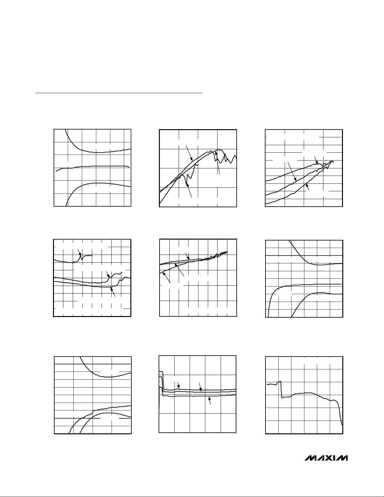
Typical Operating Characteristics
(Circuit of Figure 1, adapter = 19.5V, ChargeVoltage() = 16.8V, ChargeCurrent() = 3.854A, InputCurrent() = 3.584A, TA = +25°C,
unless otherwise noted.)
INPUT CURRENT-LIMIT ERROR
vs. INPUT CURRENT-LIMIT SETTING
INPUT CURRENT-LIMIT SETTING (A)
INPUT CURRENT-LIMIT ERROR (%)
MAX8731 toc01
0246810
-6
-2
-4
0
2
4
6
MAXIMUM
MINIMUM
TYPICAL
INPUT CURRENT-LIMIT ERROR
vs. SYSTEM CURRENT
SYSTEM CURRENT (A)
INPUT CURRENT-LIMIT ERROR (%)
MAX8731 toc02
01234
-0.4
-0.2
0
0.2
0.4
INPUT CURRENT LIMIT = 2.048A
INPUT CURRENT LIMIT = 3.584A
INPUT CURRENT
LIMIT = 4.096A
INPUT CURRENT-LIMIT ERROR
vs. SYSTEM CURRENT
SYSTEM CURRENT (A)
INPUT CURRENT-LIMIT ERROR (%)
MAX8731 toc03
01234
-1.0
-0.8
-0.6
-0.4
-0.2
0
0.2
0.4
0.6
0.8
1.0
V
BATT
= 8.4V
V
BATT
= 16.8V
V
BATT
= 12.6V
INPUT CURRENT LIMIT = 3.584A
IINP ERROR vs. SYSTEM CURRENT
SYSTEM CURRENT (A)
IINP ERROR (%)
MAX8731 toc04
01.00.5 2.01.5 2.5 3.0 3.5 4.0
-1.0
-0.8
-0.6
-0.4
-0.2
0
0.2
0.4
0.6
0.8
1.0
INPUT CURRENT LIMIT = 2.048A
INPUT CURRENT LIMIT = 3.584A
INPUT CURRENT LIMIT = 4.096A
OPERATING AT INPUT CURRENT LIMIT
IINP ERROR vs. SYSTEM CURRENT
SYSTEM CURRENT (A)
IINP ERROR (%)
MAX8731 toc05
01234
0
0.5
1.0
1.5
2.0
2.5
V
BATT
= 8.4V
V
BATT
= 12.6V
V
BATT
= 16.8V
INPUT CURRENT LIMIT = 3.584A
IINP ERROR vs. INPUT CURRENT
INPUT CURRENT (A)
IINP ERROR (%)
MAX8731 toc06
0123456
-10
-6
-8
-2
2
6
-4
0
4
8
10
MAXIMUM
MINIMUM
TYPICAL
NOT SWITCHING
CHARGE-CURRENT ERROR vs.
CHARGE CURRENT-LIMIT SETTING
CHARGE-CURRENT SETTING (A)
CHARGE-CURRENT LIMIT ERROR (%)
MAX8731 toc07
024 86
-10
-6
-8
-2
2
6
-4
0
4
8
10
MAXIMUM
MINIMUM
TYPICAL
CHARGE-CURRENT ERROR
vs. BATTERY VOLTAGE
BATTERY VOLTAGE (V)
CHARGE-CURRENT ERROR (%)
MAX8731 toc08
3 6 9 12 15 18
-4
-2
0
2
4
3.072A
3.968A
8.064A
TRICKLE-CHARGE CURRENT ERROR
vs. BATTERY VOLTAGE
BATTERY VOLTAGE (V)
TRICKLE-CHARGE CURRENT ERROR (%)
MAX8731 toc09
0 3 6 9 12 15 18
-30
-25
-20
-15
-10
-5
0
ChargeCurrent( ) = 128mA

CHARGE-VOLTAGE ERROR
vs. CHARGE-VOLTAGE SETTING
CHARGE-VOLTAGE SETTING (V)
CHARGE-VOLTAGE ERROR (%)
MAX8731 toc10
4 8 12 16 20
-0.6
-0.4
-0.2
0.0
0.2
0.4
0.6
BATTERY-VOLTAGE ERROR
vs. CHARGE CURRENT
CHARGE CURRENT (A)
BATTERY-VOLTAGE ERROR (%)
MAX8731 toc11
0123456
-0.3
-0.2
-0.1
0.0
0.1
0.2
0.3
3 CELLS
2 CELLS
4 CELLS
BATTERY REMOVAL
20µs/div
MAX8731 toc12
13.5V
13.0V
12.5V
V
OUT
OUTPUT CAPACITOR = 22µF
ChargeVoltage( ) = 12.6V
V
OUT
OUTPUT CAPACITOR = 10µF
SYSTEM LOAD TRANSIENT
200µs/div
MAX8731toc13
LOAD
CURRENT
ADAPTER
CURRENT
INDUCTOR
CURRENT
CCS VOLTAGE
500 mV/div
CCI VOLTAGE
500 mV/div
5A
0A
0A
5A
5A
0A
500mV/div
500mV/div
CCI
CCS
CCI
CCS
EFFICIENCY vs. CHARGE CURRENT
CHARGE CURRENT (A)
EFFICIENCY (%)
MAX8731 toc14
02468
60
65
70
75
80
85
90
95
100
2 CELLS
3 CELLS
4 CELLS
LDO LOAD REGULATION
I
LDO
(mA)
LDO ERROR (mV)
MAX8731 toc15
0 20406080100
-40
-35
-30
-25
-20
-15
-10
-5
0
CHARGER OFF
MAX8731
SMBus Level 2 Battery Charger with
Remote Sense
______________________________________________________________________________________ 11
Typical Operating Characteristics (continued)
(Circuit of Figure 1, adapter = 19.5V, ChargeVoltage() = 16.8V, ChargeCurrent() = 3.854A, InputCurrent() = 3.584A, TA = +25°C,
unless otherwise noted.)

Typical Operating Characteristics (continued)
(Circuit of Figure 1, adapter = 19.5V, ChargeVoltage() = 16.8V, ChargeCurrent() = 3.854A, InputCurrent() = 3.584A, TA = +25°C,
unless otherwise noted.)
MAX8731
SMBus Level 2 Battery Charger with
Remote Sense
12 ______________________________________________________________________________________
0
LDO LINE REGULATION
-1
-2
-3
LDO ERROR (mV)
-4
-5
-6
8 131823
V
DCIN
450
400
350
300
FREQUENCY (kHz)
250
200
NOT SWITCHING
(V)
SWITCHING FREQUENCY
MAX8731 toc16
0.20
0.15
0.10
0.05
0
-0.05
REF ERROR (%)
-0.10
-0.15
-0.20
0 0.2 0.4 0.6 0.8 1.0
MAX8731 toc19
I
(mA)
REF
NOT SWITCHING
CHARGE CURRENT (A)
REF LOAD REGULATION
5
BATTERY-CHARGE CURVE
2.8Ah x 3S3P BATTERY
4
3
2
1
MAX8731 toc17
REF ERROR vs. TEMPERATURE
0.3
0.2
0.1
0.0
REF ERROR (%)
-0.1
-0.2
-0.3
-40-200 20406080
TEMPERATURE (°C)
MAX8731 toc20
BATTERY VOLTAGE
CHARGE CURRENT
13.0
12.5
12.0
11.5
11.0
BATTERY VOLTAGE (V)
10.5
MAX8731 toc18
150
0 5 10 15 20
V
- V
ADAPTER
BATTERY
ADAPTER CURRENT
vs. ADAPTER VOLTAGE
3.0
SWITCHING, NO LOAD
2.5
2.0
1.5
1.0
ADAPTER CURRENT (mA)
0.5
0
0 5 10 15 20 25 30
ChargeVoltage( ) = 4.192V
NOT SWITCHING
ADAPTER VOLTAGE (V)
(V)
MAX8731 toc21
0
0123456
TIME (h)
BATTERY-LEAKAGE CURRENT
vs. BATTERY VOLTAGE
2.5
ADAPTER PRESENT OR ABSENT
2.0
1.5
1.0
BATTERY CURRENT (µA)
0.5
0
0 5 10 15 20
BATTERY VOLTAGE (V)
10.0
MAX8731 toc22

MAX8731
SMBus Level 2 Battery Charger with
Remote Sense
______________________________________________________________________________________ 13
Pin Description
PIN NAME FUNCTION
1, 12 GND Analog Ground. Connect directly to the paddle.
2 ACIN AC Adapter Detect Input. ACIN is the input to an uncommitted comparator.
3 REF 4.096V Voltage Reference. Bypass REF with a 1µF capacitor to GND.
4 CCS Input Current Regulation Loop-Compensation Point. Connect 0.01µF from CCS to GND.
5 CCI Output Current Regulation Loop-Compensation Point. Connect 0.01µF from CCI to GND.
6 CCV Voltage Regulation Loop-Compensation Point. Connect 10kΩ in series with 0.01µF to GND.
7 DAC DAC Voltage Output. Bypass with 0.1µF from DAC to GND.
8 IINP
9 SDA S M Bus D ata I/O. Op en- d r ai n outp ut. C onnect an exter nal p ul l up r esi stor accor d i ng to S M Bus sp eci fi cati ons.
10 SCL SMBus Clock Input. Connect an external pullup resistor according to SMBus specifications.
11 V
DD
13 ACOK
14 BATSEL
15 FBSA
16 FBSB
17 CSIN Charge Current-Sense Negative Input
18 CSIP C har g e C ur r ent- S ense P osi ti ve I np ut. C onnect a 10m Ω cur r ent- sense r esi stor b etw een C S IP and C S IN .
19 PGND Power Ground
20 DLO
Input Current Monitor Output. IINP sources the current proportional to the current sensed across
CSSP and CSSN. The transconductance from (CSSP - CSSN) to IINP is 3mA/V.
Logic Circuitry Supply-Voltage Input. Bypass with a 0.1µF capacitor to GND.
AC D etect Outp ut. Thi s op en- d r ai n outp ut i s hi g h i m p ed ance w hen AC IN i s g r eater than RE F/2. The
AC O K outp ut r em ai ns l ow w hen the M AX 8731 i s p ow er ed d ow n. C onnect a 10kΩ p ul l up r esi stor fr om
V
to AC O K.
C C
Batter y V ol tag e S el ect Inp ut. D r i ve BATS E L hi g h to sel ect b atter y B, or d r i ve BATS E L l ow to sel ect b atter y A.
Any chang e of BATS E L i m m ed i atel y stop s char g i ng . C har g i ng b eg i ns ag ai n i n ap p r oxi m atel y 10m s.
Remote Sense Input for the Output Voltage of Battery A. Connect a 100Ω resistor from FBSA to the
battery connector, and a 10nF capacitor from FBSA to PGND.
Remote Sense Input for the Output Voltage of Battery B. Connect a 100Ω resistor from FBSB to the
battery connector, and a 10nF capacitor from FBSB to PGND.
Low-Side Power MOSFET Driver Output. Connect to low-side n-channel MOSFET. DLO drives
between LDO and PGND.
Linear-Regulator Output. LDO is the output of the 5.4V linear regulator supplied from DCIN. LDO also
21 LDO
directly supplies the DLO driver and the BST charge pump. Bypass with a 1µF ceramic capacitor
from LDO to PGND.
22 DCIN Charger Bias Supply Input. Bypass DCIN with a 0.1µF capacitor to PGND.
23 LX
H i g h- S i d e P ow er M OS FE T D r i ver S our ce C onnecti on. C onnect to the sour ce of the hi g h- si d e n- channel
M OS FE T.
24 DHI High-Side Power MOSFET Driver Output. Connect to the high-side n-channel MOSFET gate.
25 BST H i g h- S i d e P ow er M OS FE T D r i ver P ow er - S up p l y C onnecti on. C onnect a 0.1µF cap aci tor fr om BS T to LX .
26 V
CC
D evi ce P ow er - S up p l y I np ut. C onnect to LD O thr oug h an RC fi l ter as show n i n Fi g ur e 1.
27 CSSN Input Current-Sense Negative Input
28 CSSP Inp ut C ur r ent- S ense P osi ti ve Inp ut. C onnect a 10m Ω cur r ent- sense r esi stor b etw een C S S P and C S S N .
29 BP Backside Paddle. Connect the backside paddle to analog ground.

MAX8731
SMBus Level 2 Battery Charger with
Remote Sense
14 ______________________________________________________________________________________
Figure 1. Typical Dual-Battery Application Circuit
Detailed Description
The typical operating circuit is shown in Figure 1. The
MAX8731 includes all the functions necessary to
charge Li+, NiMH, and NiCd smart batteries. A highefficiency, synchronous-rectified, step-down DC-DC
converter is used to implement a precision constantcurrent, constant-voltage charger. The DC-DC converter drives a high-side n-channel MOSFET and provides
synchronous rectification with a low-side n-channel
MOSFET. The charge current and input current-sense
amplifiers have low input-offset error (±64µV typ),
allowing the use of small-valued sense resistors.
The MAX8731 features a voltage-regulation loop (CCV)
and two current-regulation loops (CCI and CCS). The
loops operate independently of each other. The CCV
voltage-regulation loop monitors either FBSA or FBSB
to ensure that its voltage never exceeds the voltage set
by the ChargeVoltage() command. The CCI battery current-regulation loop monitors current delivered to the
selected battery to ensure that it never exceeds the
current limit set by the ChargeCurrent() command. The
ADAPTER
INPUT
R2
0.1µF
0.1µF
0.01µF
C6
0.01µF
100kΩ
MAX8731
C8
0.1µF
BATSEL
BP
CSSP
CSSN
V
LDO
BST
DHI
DLO
PGND
CSIP
CSIN
FBSB
FBSA
GND
RS1
10mΩ
CC
C12
1µF
R12
33Ω
LDO
C11
D2
1µF
N1, N2,: SI4800BDY
N3: SI4810BDY
C10
0.1µF
N1
R11
LDO
R10
100Ω
R9
100Ω
C9
220pF
D3
R13
1kΩ
1Ω
N3
SELECTOR
BATTERY
A
LX
C
IN1
10µF
DHI
L1
4.3µH
L1: SUMIDA
CEP125-4R3MC-U
RS2
10mΩ
V
OUT
C
OUT1
10µF
BATTERY
B
SYSTEM
LOAD
C
IN2
10µF
N2
DCIN
ACIN
ACOK
V
DD
SCL
C2
SDA
IINP
C3
CCV
C7
1µF
CCI
CCS
REF
DAC
C5
KBC
D1
C1
1µF
INPUT
VDD
SCL
SDA
150kΩ
49.9kΩ
LDO
10kΩ
10kΩ
C4
0.01µF
R1
R3
R5
R8
R4
10kΩ
10kΩ
R6
R7
10kΩ
N
C
OUT2
10µF

MAX8731
SMBus Level 2 Battery Charger with
Remote Sense
______________________________________________________________________________________ 15
Figure 2. Functional Diagram
charge current-regulation loop is in control as long as
the selected battery voltage is below the charge voltage set point. When the selected battery voltage reaches its set point, the voltage-regulation loop takes control
and maintains the battery voltage at the set point. A
third loop (CCS) takes control and reduces the charge
current when the adapter current exceeds the input
current limit set by the InputCurrent() command.
A functional diagram is shown in Figure 2.
ACIN
ACOK
GND
CCV
CCI
CCS
MAX8731
CSSP
CSIN
VCC
CSA: CURRENT-SENSE
AMPLIFIER
GM
REF/2
LOWEST VOLTAGE CLAMP
GMS
CSS
CSA
POWER-FAIL
LVC
CSI
CSA
A = 20V/V
(750mA FOR RS2 = 10mΩ)
100mV
GMI
150mV
A = 1V/V
ZCMD
ENABLE
IMIN
CCMP
GMV
DC-DC
CONVERTER
CHARGE VOLTAGE( )
11-BIT DAC
IMAX
OVP
+100mV
6-BIT DAC
6-BIT DAC
2V
(10A FOR RS2 = 10mΩ)
HIGHSIDE
DRIVER
LEVEL
SHIFT
LOWSIDE
DRIVER
5.4V
LINEAR
REGULATOR
4.096V
REFERENCE
SMBus LOGIC
CHARGE VOLTAGE ( )
CHARGE CURRENT ( )
INPUT CURRENT ( )
BST
DHI
LX
LDO
DLO
PGND
DCIN
V
CC
REF
SCL
SDA
V
DD
IINP
CSSN
A = 20V/V
CSSP
CSIP
CSIN
BATSEL
FBSB
FBSA
DAC

MAX8731
SMBus Level 2 Battery Charger with
Remote Sense
16 ______________________________________________________________________________________
Table 1. ChargeVoltage () (0x15)
Setting Charge Voltage
To set the output voltage, use the SMBus to write a 16bit ChargeVoltage() command using the data format
listed in Table 1. The ChargeVoltage() command uses
the Write-Word protocol (see Figure 3). The command
code for ChargeVoltage() is 0x15 (0b00010101). The
MAX8731 provides a 1.024V to 19.200V charge voltage
range, with 16mV resolution. Set ChargeVoltage()
below 1.024V to terminate charging. Upon reset, the
ChargeVoltage() and ChargeCurrent() values are
cleared and the charger remains off until both the
ChargeVoltage() and the ChargeCurrent() command
are sent. Both DHI and DLO remain low until the charger is restarted.
BIT BIT NAME DESCRIPTION
0 — Not used. Normally a 1mV weight.
1 — Not used. Normally a 2mV weight.
2 — Not used. Normally a 4mV weight.
3 — Not used. Normally a 8mV weight.
4 Charge voltage, DACV 0
5 Charge voltage, DACV 1
6 Charge voltage, DACV 2
7 Charge voltage, DACV 3
8 Charge voltage, DACV 4
9 Charge voltage, DACV 5
10 Charge voltage, DACV 6
11 Charge voltage, DACV 7
12 Charge voltage, DACV 8
13 Charge voltage, DACV 9
14 Charge voltage, DACV 10
15 — Not used. Normally a 32,768mV weight.
0 = Adds 0mV of charger voltage compliance, 1024mV min.
1 = Adds 16mV of charger voltage compliance.
0 = Adds 0mV of charger voltage compliance, 1024mV min.
1 = Adds 32mV of charger voltage compliance.
0 = Adds 0mV of charger voltage compliance, 1024mV min.
1 = Adds 64mV of charger voltage compliance.
0 = Adds 0mV of charger voltage compliance, 1024mV min.
1 = Adds 128mV of charger voltage compliance.
0 = Adds 0mV of charger voltage compliance, 1024mV min.
1 = Adds 256mV of charger voltage compliance.
0 = Adds 0mV of charger voltage compliance, 1024mV min.
1 = Adds 512mV of charger voltage compliance.
0 = Adds 0mA of charger voltage compliance.
1 = Adds 1024mV of charger voltage compliance.
0 = Adds 0mV of charger voltage compliance.
1 = Adds 2048mV of charger voltage compliance.
0 = Adds 0mV of charger voltage compliance.
1 = Adds 4096mV of charger voltage compliance.
0 = Adds 0mV of charger voltage compliance.
1 = Adds 8192mV of charger voltage compliance.
0 = Adds 0mV of charger voltage compliance.
1 = Adds 16,384mV of charger voltage compliance, 19,200mV max.

MAX8731
SMBus Level 2 Battery Charger with
Remote Sense
______________________________________________________________________________________ 17
Table 2. ChargeCurrent() (0x14) (10mΩ Sense Resistor, RS2)
Setting Charge Current
To set the charge current, use the SMBus to write a 16bit ChargeCurrent() command using the data format
listed in Table 2. The ChargeCurrent() command uses
the Write-Word protocol (see Figure 3). The command
code for ChargeCurrent() is 0x14 (0b00010100). When
RS2 =10mΩ, the MAX8731 provides a charge current
range of 128mA to 8.064A, with 128mA resolution. Set
ChargeCurrent() to 0 to terminate charging. Upon reset,
the ChargeVoltage() and ChargeCurrent() values are
cleared and the charger remains off until both the
ChargeVoltage() and the ChargeCurrent() commands
are sent. Both DHI and DLO remain low until the charger
is restarted.
The MAX8731 includes a foldback current limit when
the battery voltage is low. If the battery voltage is less
than 2.5V, the charge current is temporarily set to
128mA. The ChargeCurrent() register is preserved and
becomes active again when the battery voltage is higher than 2.5V. This function effectively provides a foldback current limit, which protects the charger during
short circuit and overload.
Setting Input Current Limit
System current normally fluctuates as portions of the
system are powered up or put to sleep. By using the
input-current-limit circuit, the output-current requirement of the AC wall adapter can be lowered, reducing
system cost.
The total input current, from a wall cube or other DC
source, is the sum of the system supply current and the
current required by the charger. When the input current
exceeds the set input current limit, the MAX8731
decreases the charge current to provide priority to system load current. As the system supply rises, the available charge current drops linearly to zero. Thereafter,
the total input current can increase without limit.
The internal amplifier compares the differential voltage
between CSSP and CSSN to a scaled voltage set by
the InputCurrent() command (see Table 3). The total
input current is the sum of the device supply current,
the charger input current, and the system load current.
The total input current can be estimated as follows:
BIT BIT NAME DESCRIPTION
0 — Not used. Normally a 1mA weight.
1 — Not used. Normally a 2mA weight.
2 — Not used. Normally a 4mA weight.
3 — Not used. Normally an 8mA weight.
4 — Not used. Normally a 16mA weight.
5 — Not used. Normally a 32mA weight.
6 — Not used. Normally a 64mA weight.
7 Charge Current, DACI 0
8 Charge Current, DACI 1
9 Charge Current, DACI 2
10 Charge Current, DACI 3
11 Charge Current, DACI 4
12 Charge Current, DACI 5
13 — Not used. Normally a 8192mA weight.
14 — Not used. Normally a 16,386mA weight.
15 — Not used. Normally a 32,772mA weight.
0 = Adds 0mA of charger current compliance.
1 = Adds 128mA of charger current compliance.
0 = Adds 0mA of charger current compliance.
1 = Adds 256mA of charger current compliance.
0 = Adds 0mA of charger current compliance.
1 = Adds 512mA of charger current compliance.
0 = Adds 0mA of charger current compliance.
1 = Adds 1024mA of charger current compliance.
0 = Adds 0mA of charger current compliance.
1 = Adds 2048mA of charger current compliance.
0 = Adds 0mA of charger current compliance.
1 = Adds 4096mA of charger current compliance, 8064mA max.

MAX8731
SMBus Level 2 Battery Charger with
Remote Sense
18 ______________________________________________________________________________________
Table 3. InputCurrent() (0x3F) (10mΩ Sense Resistor, RS1)
where η is the efficiency of the DC-DC converter (typically 85% to 95%).
To set the input current limit, use the SMBus to write a
16-bit InputCurrent() command using the data format
listed in Table 3. The InputCurrent() command uses the
Write-Word protocol (see Figure 3). The command
code for InputCurrent() is 0x3F (0b00111111). When
RS1 = 10mΩ, the MAX8731 provides an input-currentlimit range of 256mA to 11.004A, with 256mA resolution. InputCurrent() settings from 1mA to 256mA result
in a current limit of 256mA. Upon reset the input current
limit is 256mA.
Charger Timeout
The MAX8731 includes a timer to terminate charging if
the charger does not receive a ChargeVoltage() or
ChargeCurrent() command within 175s. If a timeout
occurs, both ChargeVoltage() and ChargeCurrent()
commands must be resent to reenable charging.
Remote Sense
The MAX8731 features dual remote sense, which allows
the rejection of board resistance and selector resistance
when used in either single- or dual-battery systems. To
fully utilize remote sensing, connect FBS_ directly to the
battery interface through an unshared battery sense
trace in series with a 100Ω resistor, and 10nF capacitor
(see Figure 1). In single-battery systems, connect
BATSEL directly to GND and use only FBSA.
Remote sensing cancels the effect of impedance in
series with the battery. This impedance normally causes the battery charger to prematurely enter constantvoltage mode with reducing charge current. The result
is that the last 20% of charging takes longer than necessary. When in constant-voltage mode, the remaining
charge time is proportional to the total resistance in
series with the battery. Remote sensing reduces
charge time according to the following equation:
⎣
⎦
⎡
IV
()
II
=+
INPUT LOAD
CHARGE BATTERY
⎢
⎢
×
η
×
V
()
IN
⎤
+
I
⎥
BIAS
⎥
BIT BIT NAME DESCRIPTION
0 — Not used. Normally a 2mA weight.
1 — Not used. Normally a 4mA weight.
2 — Not used. Normally an 8mA weight.
3 — Not used. Normally a 16mA weight.
4 — Not used. Normally a 32mA weight.
5 — Not used. Normally a 64mA weight.
6 — Not used. Normally a 128mA weight.
7 Input Current, DACS 0
8 Input Current, DACS 1
9 Input Current, DACS 2
10 Input Current, DACS 3
11 Input Current, DACS 4
12 Input Current, DACS 5
13 — Not used. Normally a 16,384mA weight.
14 — Not used. Normally a 32,768mA weight.
15 — Not used. Normally a 65,536mA weight.
0 = Adds 0mA of input current compliance.
1 = Adds 256mA of input current compliance.
0 = Adds 0mA of input current compliance.
1 = Adds 512mA of input current compliance.
0 = Adds 0mA of input current compliance.
1 = Adds 1024mA of input current compliance.
0 = Adds 0mA of input current compliance.
1 = Adds 2048mA of input current compliance.
0 = Adds 0mA of input current compliance.
1 = Adds 4096mA of input current compliance.
0 = Adds 0mA of input current compliance.
1 = Adds 8192mA of input current compliance, 11,004mA max.
tt
=×
CVRS CV
0
R
Pack
+
RR
Pack Board

MAX8731
SMBus Level 2 Battery Charger with
Remote Sense
______________________________________________________________________________________ 19
where R
Pack
is the total resistance in the battery pack,
R
Board
is the board resistance in series with the battery
charge path, t
CV0
is the constant-voltage charge time
without remote sense, and t
CVRS
is the constant-volt-
age charge time with remote sense.
The MAX8731 includes a safety feature, which limits the
charge voltage when FBS_ or the selector is disconnected. The MAX8731 guarantees that CSIN does not
regulate more than 200mV above the selected charging voltage. This also limits the extent to which remote
sense can cancel charge-path impedance.
Input Current Measurement
Use IINP to monitor the system-input current sensed
across CSSP and CSSN. The voltage at IINP is proportional to the input current by the equation:
V
IINP
= I
INPUT
x RS1 x G
IINP
x R8
where I
INPUT
is the DC current supplied by the AC
adapter, G
IINP
is the transconductance of IINP (3mA/V
typ), and R8 is the resistor connected between IINP
and ground. Typically, IINP has a 0 to 3.5V output voltage range. Leave IINP open if not used.
LDO Regulator
An integrated low-dropout (LDO) linear regulator provides a 5.4V supply derived from DCIN, and delivers over
30mA of load current. The LDO powers the gate drivers
of the n-channel MOSFETs. See the MOSFET Drivers
section. LDO has a minimum current limit of 35mA. This
allows the MAX8731 to work with 87nC of total gate
charge (both high-side and low-side MOSFETs). Bypass
LDO to PGND with a 1µF or greater ceramic capacitor.
AC Adapter Detection
The MAX8731 includes a hysteretic comparator that
detects the presence of an AC power adapter. When
ACIN is greater than 2.048V, the open-drain ACOK output becomes high impedance. Connect 10kΩ pullup
resistance between LDO and ACOK. Use a resistive
voltage-divider from the adapter’s output to the ACIN
pin to set the appropriate detection threshold. Select
the resistive voltage-divider not to exceed the 6V
absolute maximum rating of ACIN.
VDDSupply
The VDDinput provides power to the SMBus interface.
Connect VDDto LDO, or apply an external supply to
VDDto keep the SMBus interface active while the supply to DCIN is removed. When V
DD
is biased the internal registers are maintained. Bypass VDDto GND with
a 0.1µF or greater ceramic capacitor.
Operating Conditions
The MAX8731 has the following operating states:
• Adapter Present: When DCIN is greater than 7.5V,
the adapter is considered to be present. In this condition, both the LDO and REF function properly and
battery charging is allowed:
a) Charging: The total MAX8731 quiescent current
when charging is 1mA (max) plus the current required
to drive the MOSFETs.
b) Not Charging: To disable charging, set either
ChargeCurrent() or ChargeVoltage() to zero. When the
adapter is present and charging is disabled, the total
adapter quiescent current is less than 1mA and the
total battery quiescent current is less than 5µA.
• Adapter Absent (Power Fail): When V
CSSP
is less
than V
CSIN
+ 10mV, the MAX8731 is in the power-fail
state, since the DC-DC converter is in dropout. The
charger does not attempt to charge in the power-fail
state. Typically, this occurs when the adapter is
absent. When the adapter is absent, the total MAX8731
quiescent battery current is less than 1µA (max).
•V
DD
Undervoltage (POR): When VDDis less than
2.5V, the V
DD
supply is in an undervoltage state and
the internal registers are in their POR state. The
SMBus interface does not respond to commands.
When VDDrises above 2.5V, the MAX8731 is in a
power-on reset state. Charging does not occur until
the ChargeVoltage() and ChargeCurrent() commands are sent. When V
DD
is greater than 2.5V,
SMBus registers are preserved.
The MAX8731 allows charging under the following conditions:
1) DCIN > 7.5V, LDO > 4V, REF > 3.1V
2) V
CSSP
> V
CSIN
+ 210mV (15mV falling threshold)
3) VDD> 2.5V

MAX8731
SMBus Level 2 Battery Charger with
Remote Sense
20 ______________________________________________________________________________________
Figure 3. SMBus Write-Word and Read-Word Protocols
SMBus Interface
The MAX8731 receives control inputs from the SMBus
interface. The MAX8731 uses a simplified subset of the
commands documented in System Management Bus
Specification V1.1, which can be downloaded from
www.smbus.org. The MAX8731 uses the SMBus ReadWord and Write-Word protocols (Figure 3) to communicate with the smart battery. The MAX8731 performs
only as an SMBus slave device with address
0b0001001_ (0x12) and does not initiate communication on the bus. In addition, the MAX8731 has two identification (ID) registers (0xFE): a 16-bit device ID
register and a 16-bit manufacturer ID register (0xFF).
The data (SDA) and clock (SCL) pins have Schmitt-trigger inputs that can accommodate slow edges. Choose
pullup resistors (10kΩ) for SDA and SCL to achieve rise
times according to the SMBus specifications.
Communication starts when the master signals a
START condition, which is a high-to-low transition on
SDA, while SCL is high. When the master has finished
communicating, the master issues a STOP condition,
which is a low-to-high transition on SDA, while SCL is
high. The bus is then free for another transmission.
Figures 4 and 5 show the timing diagram for signals on
the SMBus interface. The address byte, command
byte, and data bytes are transmitted between the
START and STOP conditions. The SDA state changes
only while SCL is low, except for the START and STOP
conditions. Data is transmitted in 8-bit bytes and is
sampled on the rising edge of SCL. Nine clock cycles
are required to transfer each byte in or out of the
MAX8731 because either the master or the slave
acknowledges the receipt of the correct byte during the
ninth clock cycle. The MAX8731 supports the charger
commands as described in Table 4.
a) Write-Word Format
SLAVE
S
ADDRESS
7 BITS 8 BITS1b
MSB LSB MSB LSB
PRESET TO
0b0001001
b) Read-Word Format
SLAVE
S
ADDRESS
7 BITS 8 BITS1b
MSB LSB
Preset to
0b0001001
W ACK ACK ACK P
W ACK ACK NACK P
COMMAND
BYTE
ChargerMode() = 0x12
ChargeCurrent() = 0x14
ChargeVoltage() = 0x15
AlarmWarning() = 0x16
InputCurrent() = 0x3F
COMMAND
BYTE
ChargerSpecInfo() = 0x11
ChargerStatus() = 0x13
LOW DATA
ACK
BYTE
8 BITS
1b
MSB LSB
0
D7 D0 D15 D8
SLAVE
SACK
ADDRESS
1b
0
7 BITS
MSB LSBMSB LSB
PRESET TO
0b0001001
1b
0
R ACK
1b11b
HIGH DATA
BYTE
8 BITS
MSB LSB01b0
0
1b
0
LOW DATA
BYTE
8 BITS
MSB LSB
D7 D0 D15 D8
1b
0
HIGH DATA
BYTE
8 BITS
MSB LSB01b0
1b
1
LEGEND:
S = START CONDITION OR REPEATED START CONDITION
ACK = ACKNOWLEDGE (LOGIC-LOW)
W = WRITE BIT (LOGIC-LOW)
MASTER TO SLAVE
SLAVE TO MASTER
P = STOP CONDITION
NACK = NOT ACKNOWLEDGE (LOGIC-HIGH)
R = READ BIT (LOGIC-HIGH)

MAX8731
SMBus Level 2 Battery Charger with
Remote Sense
______________________________________________________________________________________ 21
Figure 4. SMBus Write Timing
Figure 5. SMBus Read Timing
AB CDEFG HIJ
t
LOWtHIGH
SMBCLK
SMBDATA
t
t
HD:STA
SU:STA
A = START CONDITION
B = MSB OF ADDRESS CLOCKED INTO SLAVE
C = LSB OF ADDRESS CLOCKED INTO SLAVE
D = R/W BIT CLOCKED INTO SLAVE
E = SLAVE PULLS SMBDATA LINE LOW
AB CDEFG H
t
LOW
t
HIGH
t
t
SU:DAT
HD:DAT
F = ACKNOWLEDGE BIT CLOCKED INTO MASTER
G = MSB OF DATA CLOCKED INTO SLAVE
H = LSB OF DATA CLOCKED INTO SLAVE
I = SLAVE PULLS SMBDATA LINE LOW
t
HD:DAT
K
J = ACKNOWLEDGE CLOCKED INTO MASTER
K = ACKNOWLEDGE CLOCK PULSE
L = STOP CONDITION, DATA EXECUTED BY SLAVE
M = NEW START CONDITION
I
t
SU:STO
L
t
BUF
J
K
M
SMBCLK
SMBDATA
t
SU:STAtHD:STA
A = START CONDITION
B = MSB OF ADDRESS CLOCKED INTO SLAVE
C = LSB OF ADDRESS CLOCKED INTO SLAVE
D = R/W BIT CLOCKED INTO SLAVE
t
SU:DAT
t
HD:DAT
E = SLAVE PULLS SMBDATA LINE LOW
F = ACKNOWLEDGE BIT CLOCKED INTO MASTER
G = MSB OF DATA CLOCKED INTO MASTER
H = LSB OF DATA CLOCKED INTO MASTER
t
SU:DAT
I = ACKNOWLEDGE CLOCK PULSE
J = STOP CONDITION
K = NEW START CONDITION
t
SU:STO
t
BUF

MAX8731
SMBus Level 2 Battery Charger with
Remote Sense
22 ______________________________________________________________________________________
Battery-Charger Commands
The MAX8731 supports four battery-charger commands that use either Write-Word or Read-Word protocols, as summarized in Table 4. ManufacturerID() and
DeviceID() can be used to identify the MAX8731. On
the MAX8731, the ManufacturerID() command always
returns 0x004D and the DeviceID() command always
returns 0x0008.
DC-DC Converter
The MAX8731 employs a synchronous step-down DCDC converter with an n-channel high-side MOSFET
switch and an n-channel low-side synchronous rectifier.
The MAX8731 features a pseudo-fixed-frequency, current-mode control scheme with cycle-by-cycle current
limit. The controller’s constant off-time (t
OFF
) is calculat-
ed based on V
CSSP
, V
CSIN
, and a time constant with a
minimum value of 300ns. The MAX8731 can also operate in discontinuous-conduction mode for improved
light-load efficiency. The operation of the DC-DC controller is determined by the following four comparators
as shown in the functional diagrams in Figures 2 and 6:
The IMIN comparator triggers a pulse in discontinuous
mode when the accumulated error is too high. IMIN
compares the control signal (LVC) against 100mV (typ).
When LVC is less than 100mV, DHI and DLO are both
forced low. Indirectly, IMIN sets the peak inductor current in discontinuous mode.
The CCMP comparator is used for current-mode regu-
lation in continuous-conduction mode. CCMP compares LVC against the inductor current. The high-side
MOSFET on-time is terminated when the CSI voltage is
higher than LVC.
The IMAX comparator provides a secondary cycle-bycycle current limit. IMAX compares CSI to 2V (corresponding to 10A when RS2 = 10mΩ). The high-side
MOSFET on-time is terminated when the current-sense
signal exceeds 10A. A new cycle cannot start until the
IMAX comparator’s output goes low.
The ZCMP comparator provides zero-crossing detection during discontinuous conduction. ZCMP compares
the current-sense feedback signal to 750mA (RS2 =
10mΩ). When the inductor current is lower than the
750mA threshold, the comparator output is high and
DLO is turned off.
The OVP comparator is used to prevent overvoltage at
the output due to battery removal. OVP compares FBS_
against the set voltage (ChargeVoltage()). When FBS_
is 100mV above the set value, the OVP comparator output goes high and the high-side MOSFET on-time is terminated. DHI and DLO remain off until the OVP
condition is removed.
CCV, CCI, CCS, and LVC Control Blocks
The MAX8731 controls input current (CCS control loop),
charge current (CCI control loop), or charge voltage
(CCV control loop), depending on the operating condition. The three control loops—CCV, CCI, and CCS—are
brought together internally at the lowest voltage-clamp
(LVC) amplifier. The output of the LVC amplifier is the
feedback control signal for the DC-DC controller. The
minimum voltage at the CCV, CCI, or CCS appears at
the output of the LVC amplifier and clamps the other
control loops to within 0.3V above the control point.
COMMAND
COMMAND NAME READ/WRITE DESCRIPTION POR STATE
0x14 ChargeCurrent() Write Only 6-Bit Charge-Current Setting 0x0000
0x15 ChargeVoltage() Write Only 11-Bit Charge-Voltage Setting 0x0000
0x3F InputCurrent() Write Only 6-Bit Charge-Current Setting 0x0080
0xFE ManufacturerID() Read Only Manufacturer ID 0x004D
0xFF DeviceID() Read Only Device ID 0x0008
Table 4. Battery-Charger Command Summary
IMAX
CCMP
IMIN
ZCMP
OVP
CSI
2V
100mV
150mV
ChargeVoltage ( )
+100mV
FBS_
DCIN
CSIN
LVC
RSQ
Q
OFF-TIME
ONE-SHOT
OFF-TIME
COMPUTE
DH
DRIVER
DL
DRIVER
Figure 6. DC-DC Converter Functional Diagram

MAX8731
SMBus Level 2 Battery Charger with
Remote Sense
______________________________________________________________________________________ 23
Clamping the other two control loops close to the lowest control loop ensures fast transition with minimal
overshoot when switching between different control
loops (see the Compensation section).
Continuous-Conduction Mode
With sufficient charge current, the MAX8731’s inductor
current never crosses zero, which is defined as continuous-conduction mode. The regulator switches at
400kHz (nominal) if V
CSIN
< 0.88 x V
CSSP
. The controller starts a new cycle by turning on the high-side
MOSFET and turning off the low-side MOSFET. When
the charge-current feedback signal (CSI) is greater
than the control point (LVC), the CCMP comparator output goes high and the controller initiates the off-time by
turning off the high-side MOSFET and turning on the
low-side MOSFET. The operating frequency is governed by the off-time and is dependent upon V
CSIN
and
V
CSSP
. The off-time is set by the following equation:
The on-time can be determined using the following
equation:
where:
The switching frequency can then be calculated:
These equations describe the controller’s pseudofixed-frequency performance over the most common
operating conditions.
At the end of the fixed off-time, the controller initiates a
new cycle if the control point (LVC) is greater than
100mV and the peak charge current is less than the
cycle-by-cycle current limit. Restated another way,
IMIN must be high, IMAX must be low, and OVP must
be low for the controller to initiate a new cycle. If the
peak inductor current exceeds the IMAX comparator
threshold or the output voltage exceeds the OVP
threshold, then the on-time is terminated. The cycle-bycycle current limit effectively protects against overcurrent and short-circuit faults.
If during the off-time the inductor current goes to zero,
the ZCMP comparator output pulls high, turning off the
low-side MOSFET. Both the high- and low-side
MOSFETs are turned off until another cycle is ready to
begin. ZCOMP causes the MAX8731 to enter into discontinuous-conduction mode (see the Discontinuous
Conduction section).
There is a 0.3µs minimum off-time when the (V
CSSP
-
V
CSIN
) differential becomes too small. If V
CSIN
≥ 0.88 x
V
CSSP
, then the threshold for the 0.3µs minimum offtime is reached. The switching frequency in this mode
varies according to the equation:
Discontinuous Conduction
The MAX8731 can also operate in discontinuous-conduction mode to ensure that the inductor current is
always positive. The MAX8731 enters discontinuousconduction mode when the output of the LVC control
point falls below 100mV. This corresponds to peak
inductor current = 500mA:
charge current for RS2 = 10mΩ.
In discontinuous mode, a new cycle is not started until
the LVC voltage rises above 100mV. Discontinuousmode operation can occur during conditioning charge
of overdischarged battery packs, when the charge current has been reduced sufficiently by the CCS control
loop, or when the charger is in constant-voltage mode
with a nearly full battery pack.
ts
=×
25. µ
OFF
t
ON
I
RIPPLE
f
SW
VV
CSSP CSIN
V
CSSP
LI
×
=
RIPPLE
VV
−
CSSN BATT
Vt
×
BATT OFF
=
=
L
1
tt
+
ON OFF
−
f
=
LI
VV
CSSN BATT
×
RIPPLE
1
03. µ
s
−
+
100
I
CHG
1
=×
2
mV
×
20 2
RS
=
250
mA

MAX8731
SMBus Level 2 Battery Charger with
Remote Sense
24 ______________________________________________________________________________________
Compensation
The charge-voltage and charge-current regulation
loops are independent and compensated separately at
the CCV, CCI, and CCS.
CCV Loop Compensation
The simplified schematic in Figure 7 is sufficient to
describe the operation of the MAX8731 when the voltage loop (CCV) is in control. The required compensation network is a pole-zero pair formed with C
CV
and
RCV. The zero is necessary to compensate the pole
formed by the output capacitor and the load. R
ESR
is
the equivalent series resistance (ESR) of the charger
output capacitor (C
OUT
). RLis the equivalent charger
output load, where RL= ∆V
BATT
/ ∆I
CHG
. The equiva-
lent output impedance of the GMV amplifier, R
OGMV
, is
greater than 10MΩ. The voltage amplifier transconduc-
tance, GMV = 0.125µA/mV. The DC-DC converter
transconductance is dependent upon the charge-current sense resistor RS2:
GM
OUT
=
where A
CSI
= 20V/V, and RS2 = 10mΩ in the typical
application circuits, so GM
OUT
= 5A/V. The loop-trans-
fer function is given by:
The poles and zeros of the voltage loop-transfer function are listed from lowest frequency to highest frequency in Table 5.
Near crossover C
CV
is much lower impedance than
R
OGMV
. Since CCVis in parallel with R
OGMV
, CCVdominates the parallel impedance near crossover.
Additionally, RCVis much higher impedance than C
CV
and dominates the series combination of RCVand CCV,
so near crossover:
Figure 7. CCV Loop Diagram
NAME EQUATION DESCRIPTION
Lowest frequency pole created by CCV and GMV’s finite output resistance.
Voltage-loop compensation zero. If this zero is at the same frequency or
lower than the output pole f
P_OUT
, then the loop-transfer function
approximates a single-pole response near the crossover frequency. Choose
C
CV
to place this zero at least 1 decade below crossover to ensure
adequate phase margin.
Output
Pole
Output pole formed with the effective load resistance R
L
and the output
capacitance C
OUT
. RL influences the DC gain but does not affect the
stability of the system or the crossover frequency.
Output
Zero
Output ESR Zero. This zero can keep the loop from crossing unity gain if
f
Z_OUT
is less than the desired crossover frequency; therefore, choose a
capacitor with an ESR zero greater than the crossover frequency.
Table 5. CCV Loop Poles and Zeros
f
RC
PCV
OGMV CV
_
=
×
1
2πfRC
ZCV
CV CV
_
=
×
1
2π
f
RC
P OUT
L OUT
_
=
×
1
2π
f
RC
P OUT
L OUT
_
=
×
1
2π
FBS_
ChargeVoltage( )
ESR
C
OUT
CCV
R
C
GM
OUT
GMV
CV
CV
R
OGMV
R
LR
1
×
CSI
2ARS
LTF GM R GMV R
=×××
OUT L OGMV
sC R sC R
+×+×
()()
11
×
OUT ESR CV CV
sC R sC R
+× + ×
()()
11
CV OGMV OUT L
RsCR
OGMV CV CV
()
1
+×
×
()
1
sC R
+×
CV OGMV
R
≅
CV
CCV Pole
CCV Zero

MAX8731
SMBus Level 2 Battery Charger with
Remote Sense
______________________________________________________________________________________ 25
C
OUT
is also much lower impedance than RLnear
crossover so the parallel impedance is mostly capacitive and:
If R
ESR
is small enough, its associated output zero has
a negligible effect near crossover and the loop-transfer
function can be simplified as follows:
Setting LTF = 1 to solve for the unity-gain frequency
yields:
For stability, choose a crossover frequency lower than
1/10 the switching frequency. For example, choose a
crossover frequency of 50kHz and solve for RVCusing
the component values listed in Figure 1 to yield RCV=
10kΩ:
GMV = 0.125µA/mV
GM
OUT
= 5A/V
C
OUT
= 2 x 10µF
F
OSC
= 400kHz
RL= 0.2Ω
F
CO_CV
= 50kHz
To ensure that the compensation zero adequately cancels the output pole, select f
Z_CV
≤ f
P_OUT
:
CCV≥ (RL/ RCV) C
OUT
CCV≥ 400pF (assuming 2 cells and 2A maximum
charge current.)
Figure 8 shows the Bode plot of the voltage-loop frequency response using the values calculated above.
CCI Loop Compensation
The simplified schematic in Figure 9 is sufficient to
describe the operation of the MAX8731 when the battery current loop (CCI) is in control. Since the output
capacitor’s impedance has little effect on the response
of the current loop, only a simple single pole is required
to compensate this loop. A
CSI
is the internal gain of the
current-sense amplifier. RS2 is the charge currentsense resistor (10mΩ). R
OGMI
is the equivalent output
impedance of the GMI amplifier, which is greater than
10MΩ. GMI is the charge-current amplifier transconductance = 1µA/mV. GM
OUT
is the DC-DC converter
transconductance = 5A/V.
Figure 8. CCV Loop Response Figure 9. CCI Loop Diagram
sC
≅
R
CV
OUT
OUT
1
G
MV
R
CV
×2π
C
OUT
_
10
Ω
k
≅
R
⋅
L
+×
()1
sC R sC
OUT L OUT
LTF GM
=×
OUT
fGMG
CO CV OUT MV
=××
_
π
=
GMV GM
×
R
CV
×2
Cf
OUT CO CV
×
80
60
40
20
MAGNITUDE (dB)
0
-20
-40
0.1 1M
MAG
PHASE
FREQUENCY (Hz)
0
GM
-45
PHASE (DEGREES)
-90
CCI
C
-135
100k10k1k100101
CI
R
OGMI
OUT
GMI
CSIP
ChargeCurrent( )
CSIN
RS2
CSI

MAX8731
SMBus Level 2 Battery Charger with
Remote Sense
26 ______________________________________________________________________________________
Figure 10. CCI Loop Response
Figure 11. CCS Loop Diagram
The loop-transfer function is given by:
This describes a single-pole system. Since:
the loop-transfer function simplifies to:
The crossover frequency is given by:
For stability, choose a crossover frequency lower than
1/10 the switching frequency:
CCI> 10 × GMI / (2π f
OSC
) = 4nF, for a 400kHz switch-
ing frequency.
Values for CCIgreater than 10 times the minimum value
can slow down the current-loop response. Choosing C
CI
= 10nF yields a crossover frequency of 15.9kHz. Figure
10 shows the Bode plot of the current-loop frequency
response using the values calculated above.
CCS Loop Compensation
The simplified schematic in Figure 11 is sufficient to
describe the operation of the MAX8731 when the input
current-limit loop (CCS) is in control. Since the output
capacitor’s impedance has little effect on the response
of the input current-limit loop, only a single pole is
required to compensate this loop. A
CSS
is the internal
gain of the current-sense resistor; RS1 = 10mΩ in the
typical application circuits. R
OGMS
is the equivalent
output impedance of the GMS amplifier, which is
greater than 10MΩ. GMS is the charge-current amplifier
transconductance = 1µA/mV. GMINis the DC-DC converter’s input-referred transconductance = (1/D) x
GM
OUT
= (1 / D) x 5A/V.
The loop-transfer function is given by:
Since:
the loop-transfer function simplifies to:
R
LTF GM A RS GMI
=×××
OUT CSI
2
OGMI
+
1
sR C
OGMI CI
×
GM
LTF GMI
=
OUT
+
=
sR C
ARS
×12
CSI
R
OGMI
×1
OGMI CI
f
CO CICI_
GMI
=
2π
C
LTF GM A RSI GMS
=×××
IN CSS
GM
=
IN
ARS
CSS
SR C
+×1
×12
R
OGMS
SR C
+×1
OGMS CS
LTF GMS
=
R
OGMS
OGMS CS
100
80
60
40
20
MAGNITUDE (dB)
0
-20
-40
0.1
FREQUENCY (Hz)
MAG
PHASE
0
InputCurrent( )
-45
-90
100k1k10
CCS
GMS
C
CS
R
OGMS
GM
CSS
IN
ADAPTER
INPUT
CSSP
RS1
CSSI
SYSTEM
LOAD

MAX8731
SMBus Level 2 Battery Charger with
Remote Sense
______________________________________________________________________________________ 27
The crossover frequency is given by:
For stability, choose a crossover frequency lower than
1/10 the switching frequency:
Choosing a crossover frequency of 30kHz and using
the component values listed in Figure 1 yields CCS>
5.4nF. Values for CCS greater than 10 times the minimum value may slow down the current-loop response
excessively. Figure 12 shows the Bode plot of the input
current-limit-loop frequency response using the values
calculated above.
MOSFET Drivers
The DHI and DLO outputs are optimized for driving
moderate-sized power MOSFETs. The MOSFET drive
capability is the same for both the low-side and highsides switches. This is consistent with the variable duty
factor that occurs in the notebook computer environment where the battery voltage changes over a wide
range. There must be a low-resistance, low-inductance
path from the DLO driver to the MOSFET gate to prevent shoot-through. Otherwise, the sense circuitry in the
MAX8731 interprets the MOSFET gate as “off” while
there is still charge left on the gate. Use very short,
wide traces measuring 10 to 20 squares or less
(1.25mm to 2.5mm wide if the MOSFET is 25mm from
the device). Unlike the DLO output, the DHI output uses
a 50ns (typ) delay time to prevent the low-side MOSFET
from turning on until DHI is fully off. The same considerations should be used for routing the DHI signal to the
high-side MOSFET.
The high-side driver (DHI) swings from LX to 5V above
LX (BST) and has a typical impedance of 3Ω sourcing
and 1Ω sinking. The low-side driver (DLO) swings from
DLOV to ground and has a typical impedance of 1Ω
sinking and 3Ω sourcing. This helps prevent DLO from
being pulled up when the high-side switch turns on, due
to capacitive coupling from the drain to the gate of the
low-side MOSFET. This places some restrictions on the
MOSFETs that can be used. Using a low-side MOSFET
with smaller gate-to-drain capacitance can prevent
these problems.
Design Procedure
MOSFET Selection
Choose the n-channel MOSFETs according to the maximum required charge current. The MOSFETs must be
able to dissipate the resistive losses plus the switching
losses at both V
DCIN(MIN)
and V
DCIN(MAX)
.
For the high-side MOSFET, the worst-case resistive
power losses occur at the maximum battery voltage
and minimum supply voltage:
Generally a low-gate charge high-side MOSFET is preferred to minimize switching losses. However, the
R
DS(ON)
required to stay within package power-dissipation limits often limits how small the MOSFET can be.
The optimum occurs when the switching (AC) losses
equal the conduction (R
DS(ON)
) losses. Calculating the
power dissipation in N1 due to switching losses is difficult since it must allow for difficult quantifying factors
that influence the turn-on and turn-off times. These factors include the internal gate resistance, gate charge,
threshold voltage, source inductance, and PC board
layout characteristics. The following switching-loss calculation provides a rough estimate and is no substitute
for breadboard evaluation, preferably including a verification using a thermocouple mounted on N1:
Figure 12. CCS Loop Response
f
CO CSCS_
C GMS f
=×52/( )π
CS OSC
100
80
60
40
20
MAGNITUDE (dB)
0
-20
-40
0.1
GMS
=
2π
C
FREQUENCY (Hz)
0
MAG
PHASE
-45
PHASE (DEGREES)
-90
100k 10M1k10
PD HighSide
CONDUCTION
()
PD High Side t V I f
SWITCHING Trans DCIN CHG SW
()=× × × ×
V
FBS
=××
V
CSSP
1
2
_
IR
CHG
2
DS ON
()

MAX8731
SMBus Level 2 Battery Charger with
Remote Sense
28 ______________________________________________________________________________________
where t
TRANS
is the driver’s transition time and can be
calculated as follows:
I
GATE
is the peak gate-drive current.
The following is the power dissipated due to the highside n-channel MOSFET’s output capacitance (C
RSS
):
The total high-side MOSFET power dissipation is:
Switching losses in the high-side MOSFET can become
an insidious heat problem when maximum AC adapter
voltages are applied. If the high-side MOSFET chosen
for adequate R
DS(ON)
at low-battery voltages becomes
hot when biased from V
IN(MAX)
, consider choosing
another MOSFET with lower parasitic capacitance. For
the low-side MOSFET (N2), the worst-case power dissipation always occurs at maximum input voltage:
The following additional loss occurs in the low-side
MOSFET due to the reverse-recovery charge of the
MOSFET’s body diode and the body diode conduction
losses:
The total power low-side MOSFET dissipation is:
These calculations provide an estimate and are not a substitute for breadboard evaluation, preferably including a
verification using a thermocouple mounted on the MOSFET.
Inductor Selection
The charge current, ripple, and operating frequency
(off-time) determine the inductor characteristics. For
optimum efficiency, choose the inductance according
to the following equation:
This sets the ripple current to 1/3 the charge current
and results in a good balance between inductor size
and efficiency. Higher inductor values decrease the ripple current. Smaller inductor values save cost but
require higher saturation current capabilities and
degrade efficiency.
Inductor L1 must have a saturation current rating of at
least the maximum charge current plus 1/2 the ripple
current (∆IL):
I
SAT
= I
CHG
+ (1/2) ∆IL
The ripple current is determined by:
∆IL = V
BATT
× t
OFF
/ L
where:
t
OFF
= 2.5µs (V
DCIN
- V
BATT
) / V
DCIN
for V
BATT
< 0.88
V
DCIN
or during dropout:
t
OFF
= 0.3µs for V
BATT
> 0.88 V
DCIN
⎛
t
TRANS
112
=+
⎜
IIQI
⎝
Gsrc GsnkGGATE
⎞
×≈
⎟
⎠
and f kHz
SW
400,
PD HighSide
COSS
()≈
2
VCf
××
DCIN
RSS SW
2
PD HighSide PD HighSide
() ()
++
() ()
TOTAL CONDUCTION
PD HighSide PD HighSide
SWITCHING COSS
≈
PD Low Side
CONDUCTION
()
⎛
1
=−
⎜
⎝
IR
××
CHG
FBS
V
CSSP
2
⎞
_
⎟
⎠
DS ON
()
V
Vt
BATT OFF
L
=
×03.
×
I
CHG
PD Low Side Q V f I V
() (. .)=× ×+××
QRR RR DCIN SW PEAK
2
PD Low Side PD Low Side
()
+
() ()
TOTAL CONDUCTION
PD HighSide
QRR
≈
005 04

MAX8731
SMBus Level 2 Battery Charger with
Remote Sense
______________________________________________________________________________________ 29
Input Capacitor Selection
The input capacitor must meet the ripple current
requirement (I
RMS
) imposed by the switching currents.
Nontantalum chemistries (ceramic, aluminum, or OSCON) are preferred due to their resilience to power-up
surge currents:
The input capacitors should be sized so that the temperature rise due to ripple current in continuous conduction
does not exceed approximately 10°C. The maximum ripple current occurs at 50% duty factor or V
DCIN
= 2 x
V
BATT
, which equates to 0.5 x I
CHG
. If the application of
interest does not achieve the maximum value, size the
input capacitors according to the worst-case conditions.
Output Capacitor Selection
The output capacitor absorbs the inductor ripple current
and must tolerate the surge current delivered from the
battery when it is initially plugged into the charger. As
such, both capacitance and ESR are important parameters in specifying the output capacitor as a filter and to
ensure stability of the DC-DC converter (see the
Compensation section). Beyond the stability requirements, it is often sufficient to make sure that the output
capacitor’s ESR is much lower than the battery’s ESR.
Either tantalum or ceramic capacitors can be used on the
output. Ceramic devices are preferable because of their
good voltage ratings and resilience to surge currents.
Applications Information
Smart-Battery System Background
Information
Smart-battery systems have evolved since the conception of the smart-battery system (SBS) specifications.
Originally, such systems consisted of a smart battery
and smart-battery charger that were compatible with the
SBS specifications and communicated directly with one
another using SMBus protocols. Modern systems still
employ the original commands and protocols, but often
use a keyboard controller or similar digital intelligence to
mediate the communication between the battery and the
charger (Figure 13). This arrangement permits considerable freedom in the implementation of charging algorithms at the expense of standardization. Algorithms can
vary from the simple detection of the battery with a fixed
set of instructions for charging the battery to highly complex programs that can accommodate multiple battery
configurations and chemistries. Microcontroller programs can perform frequent tests on the battery’s state
of charge and dynamically change the voltage and current applied to enhance safety. Multiple batteries can
also be utilized with a selector that is programmable over
the SMBus.
Setting Input Current Limit
The input current limit should be set based on the current capability of the AC adapter and the tolerance of
the input current limit. The upper limit of the input current threshold should never exceed the adapter’s minimum available output current. For example, if the
adapter’s output current rating is 5A ±10%, the input
current limit should be selected so that its upper limit is
less than 5A × 0.9 = 4.5A. Since the input current-limit
accuracy of the MAX8731 is ±3%, the typical value of
the input current limit should be set at 4.5A / 1.03 ≈
4.36A. The lower limit for input current must also be
considered. For chargers at the low end of the spec,
the input current limit for this example could be 4.36A ×
0.95, or approximately 4.14A.
Layout and Bypassing
Bypass DCIN with a 1µF ceramic to ground (Figure 1).
D1 protects the MAX8731 when the DC power source
input is reversed. Bypass VDD, DCIN, LDO, VCC, DAC,
and REF as shown in Figure 1.
Figure 13. Typical Smart-Battery System
AC-TO-DC
CONVERTER
(ADAPTER)
SYSTEM
POWER
SUPPLIES
II
RMS CHG
=
⎛
VV V
()
BATT DCIN BATT
⎜
⎜
⎝
V
DCIN
−
⎞
⎟
⎟
⎠
MAX8731
SMART-BATTERY
CHARGER/
POWER-SOURCE
SELECTOR
SMBus
CONTROL
SIGNALS
FOR
BATTERY
BATT+
BATT-
SYSTEM HOST
(KEYBOARD CONTROLLER)
SMART
BATTERY
SMBus
CONTROL
SIGNALS
FOR
BATTERY

MAX8731
SMBus Level 2 Battery Charger with
Remote Sense
30 ______________________________________________________________________________________
Good PC board layout is required to achieve specified
noise immunity, efficiency, and stable performance. The
PC board layout artist must be given explicit instructions—preferably, a sketch showing the placement of
the power-switching components and high-current routing. Refer to the PC board layout in the MAX8731 evaluation kit for examples. A ground plane is essential for
optimum performance. In most applications, the circuit
will be located on a multilayer board, and full use of the
four or more copper layers is recommended. Use the
top layer for high-current connections, the bottom layer
for quiet connections, and the inner layers for uninterrupted ground planes.
Use the following step-by-step guide:
1) Place the high-power connections first, with their
grounds adjacent:
a) Minimize the current-sense resistor trace
lengths, and ensure accurate current sensing
with Kelvin connections.
b) Minimize ground trace lengths in the high-cur-
rent paths.
c) Minimize other trace lengths in the high-current
paths.
Use > 5mm wide traces in the high-current
paths.
d) Connect C1 and C2 to high-side MOSFET
(10mm max length). Place the input capacitor
between the input current-sense resistor and
drain of the high-side MOSFET.
e) Minimize the LX node (MOSFETs, rectifier cath-
ode, inductor (15mm max length)). Keep LX on
one side of the PC board to reduce EMI radiation.
f) Since the return path of DHI is LX, route DHI near
LX. Optimally, LX and DHI should overlap. The
same principle is applied to DLO and PGND.
g) Ideally, surface-mount power components are
flush against one another with their ground terminals almost touching. These high-current
grounds are then connected to each other with a
wide, filled zone of top-layer copper, so they do
not go through vias. The resulting top-layer subground plane is connected to the normal innerlayer ground plane at the paddle. Other
high-current paths should also be minimized, but
focusing primarily on short ground and currentsense connections eliminates approximately 90%
of all PC board layout problems.
2) Place the IC and signal components. Keep the
main switching node (LX node) away from sensitive
analog components (current-sense traces and REF
capacitor).
Important: The IC must be no further than 10mm
from the current-sense resistors. Quiet connections
to REF, CCS, DAC, CCV, CCI, ACIN, and VCC
should be returned to a separate ground (GND)
island. The analog ground is separately worked
from power ground in Figure 1. There is very little
current flowing in these traces, so the ground island
need not be very large. When placed on an inner
layer, a sizable ground island can help simplify the
layout because the low-current connections can be
made through vias. The ground pad on the backside of the package should also be connected to
this quiet ground island.
3) Keep the gate-drive traces (DHI and DLO) as short
as possible (L < 20mm), and route them away from
the current-sense lines and REF. These traces
should also be relatively wide (W > 1.25mm).
4) Place ceramic bypass capacitors close to the IC.
The bulk capacitors can be placed further away.
Place the current-sense input filter capacitors under
the part, connected directly to the GND pin.
5) Use a single-point star ground placed directly
below the part at the PGND pin. Connect the power
ground (ground plane) and the quiet ground island
at this location.
Chip Information
TRANSISTOR COUNT: 10,234
PROCESS: BiCMOS

MAX8731
SMBus Level 2 Battery Charger with
Remote Sense
______________________________________________________________________________________ 31
Package Information
(The package drawing(s) in this data sheet may not reflect the most current specifications. For the latest package outline information
go to www.maxim-ic.com/packages
.)
MARKING
PIN # 1
I.D.
D
D/2
AAAAA
C
E/2
E
e
L
L1
0.10 C
A
0.08 C
A3
A1
(NE-1) X e
DETAIL A
L
D2
C
L
k
D2/2
e/2
e
(ND-1) X e
L
e e
b
L
DETAIL B
0.10 M C A B
E2/2
C
E2
L
PIN # 1 I.D.
0.35x45°
CC
L
QFN THIN.EPS
L
-DRAWING NOT TO SCALE-
PACKAGE OUTLINE,
16, 20, 28, 32, 40L THIN QFN, 5x5x0.8mm
21-0140
1
I
2

MAX8731
SMBus Level 2 Battery Charger with
Remote Sense
Maxim cannot assume responsibility for use of any circuitry other than circuitry entirely embodied in a Maxim product. No circuit patent licenses are
implied. Maxim reserves the right to change the circuitry and specifications without notice at any time.
32 ____________________Maxim Integrated Products, 120 San Gabriel Drive, Sunnyvale, CA 94086 408-737-7600
© 2006 Maxim Integrated Products Printed USA is a registered trademark of Maxim Integrated Products. Inc.
MAX8731
Package Information (continued)
(The package drawing(s) in this data sheet may not reflect the most current specifications. For the latest package outline information
go to www.maxim-ic.com/packages
.)
PKG.
SYMBOL
JEDEC
NOTES:
1. DIMENSIONING & TOLERANCING CONFORM TO ASME Y14.5M-1994.
2. ALL DIMENSIONS ARE IN MILLIMETERS. ANGLES ARE IN DEGREES.
3. N IS THE TOTAL NUMBER OF TERMINALS.
4. THE TERMINAL #1 IDENTIFIER AND TERMINAL NUMBERING CONVENTION SHALL
CONFORM TO JESD 95-1 SPP-012. DETAILS OF TERMINAL #1 IDENTIFIER ARE
OPTIONAL, BUT MUST BE LOCATED WITHIN THE ZONE INDICATED. THE TERMINAL #1
IDENTIFIER MAY BE EITHER A MOLD OR MARKED FEATURE.
5. DIMENSION b APPLIES TO METALLIZED TERMINAL AND IS MEASURED BETWEEN
0.25 mm AND 0.30 mm FROM TERMINAL TIP.
6. ND AND NE REFER TO THE NUMBER OF TERMINALS ON EACH D AND E SIDE RESPECTIVELY.
7. DEPOPULATION IS POSSIBLE IN A SYMMETRICAL FASHION.
8. COPLANARITY APPLIES TO THE EXPOSED HEAT SINK SLUG AS WELL AS THE TERMINALS.
9. DRAWING CONFORMS TO JEDEC MO220, EXCEPT EXPOSED PAD DIMENSION FOR
T2855-3 AND T2855-6.
10. WARPAGE SHALL NOT EXCEED 0.10 mm.
11. MARKING IS FOR PACKAGE ORIENTATION REFERENCE ONLY.
12. NUMBER OF LEADS SHOWN ARE FOR REFERENCE ONLY.
13. LEAD CENTERLINES TO BE AT TRUE POSITION AS DEFINED BY BASIC DIMENSION "e", ±0.05.
-DRAWING NOT TO SCALE-
MIN. MAX.NOM.
A
0.70 0.800.75
A1
A3
b
0.25
D
4.90
E
4.90
e
0.250--
k
L
0.30 0.500.40
L1
N
ND
NE
16L 5x5
0.02
0.20 REF.
5.00
0.80 BSC.
--16
4
4
WHHB
0.05
0.350.30
5.10
5.105.00
COMMON DIMENSIONS
20L 5x5
NOM.
MIN.
MAX.
MIN.
0.70
0.25
0.25
0
0.20 REF.
4.90
4.90
0.65 BSC.
0.45
---
0.75
0.02
0.30
5.00
5.00
0.55
20
5
5
WHHC
0.80
0.05
0.35
5.10
5.10
0.65
--
0.70
0
0.20 REF.
0.20
4.90
4.90
0.25
0.45
---
28L 5x5
NOM.
0.75
0.02
0.25
5.00
5.00
0.50 BSC.
0.55
28
7
7
WHHD-1
MAX.
MIN.
0.80
0.70
0.05
0
0.30
0.20 0.25 0.30
5.10
4.90
5.10
4.90
--
0.25
0.65
0.30
---
32L 5x5
NOM.
0.75
0.02
0.20 REF.
5.00
5.00
0.50 BSC.
0.40
32
8
8
WHHD-2
MAX.
MIN.
0.70
0.80
0.05
0.15
5.10
4.90
5.10
4.90 5.00
--
0.25 0.35 0.45
0.50
0.30
40L 5x5
NOM.
0.75 0.80
0.20 REF.
5.00 5.10
0.40 BSC.
0.40 0.50
40
10
10
-----
MAX.
0.050 0.02
0.250.20
5.10
0.600.40 0.50
EXPOSED PAD VARIATIONS
PKG.
CODES
D2
MAX.
NOM.MIN.
MIN.
E2
NOM. MAX.
T1655-2
3.203.00T1655-3 3.10 3.00 3.10 3.20 NO
T2055-4
3.103.00 3.203.103.00 3.20
3.353.15T2055-5 3.25 3.15 3.25 3.35
T2855-3 3.15 3.25 3.35 3.15 3.25 3.35
T2855-4 2.60 2.70 2.80 2.60 2.70 2.80
T2855-5 2.60 2.70 2.80 2.60 2.70 2.80
T2855-6
T2855-7 2.60 2.70
3.15 3.25 3.35 3.15 3.25 3.35
2.80
2.60 2.70 2.80
3.353.15T2855-8 3.25 3.15 3.25 3.35
3.15
3.25 3.15 3.25 3.35
T2855N-1
3.00 3.10T3255-3 3 3.203.00 3.10
T3255-5 YES3.003.103.00
3.35
3.20
3.203.00 3.10T3255-4 3 3.203.00 3.10
3.20
3.203.10T3255N-1 3.00
3.203.10
3.203.103.00
3.30T4055-1 3.20 3.40 3.20 3.30 3.40
SEE COMMON DIMENSIONS TABLE
**
PACKAGE OUTLINE,
16, 20, 28, 32, 40L THIN QFN, 5x5x0.8mm
21-0140
exceptions
±0.15
**
**
**
**
**
0.40
**
**
**
**
**
0.40
**
**
**
**
**
**
DOWN
L
BONDS
ALLOWED
YES3.203.103.003.103.00 3.20
NO3.203.103.003.10T1655N-1 3.00 3.20
YES3.103.00 3.203.103.00 3.20T2055-3
NO
YES
YES
YES
NO
NO
YES
YES
NO
YES
NO
NO
YES
2
I
2

 Loading...