

MAX872/MAX874
10µA, Low-Dropout,
Precision Voltage References
________________________________________________________________
Maxim Integrated Products
1
For free samples & the latest literature: http://www.maxim-ic.com, or phone 1-800-998-8800.
For small orders, phone 1-800-835-8769.
General Description
The MAX872/MAX874 precision 2.5V and 4.096V micropower voltage references consume a maximum of only
10µA and operate from supply voltages up to 20V. The
combination of ultra-low quiescent current and low
200mV dropout makes them ideal for battery-powered
equipment. They source and sink up to 500µA with only
200mV input voltage headroom, which makes the 2.5V
MAX872 ideal for use with a 3V supply and the 4.096V
MAX874 ideal for use with a 5V supply.
Initial accuracy of 0.2% at +25°C (±5mV for the MAX872,
±8mV for the MAX874) and low 40ppm/°C max drift make
these references suitable for a wide range of precision
applications.
Applications
Hand-Held Instruments
Battery-Operated Equipment
Power Supplies
Features
♦ Output Voltage
2.500V ±0.2% (MAX872)
4.096V ±0.2% (MAX874)
♦ Wide Operating Voltage Range
2.7V to 20V (MAX872)
4.3V to 20V (MAX874)
♦ 10µA Max Supply Current
♦ 40ppm/°C Max Drift Over Extended Temp. Range
♦ Line Regulation Over Temp.
20µV/V (MAX872)
75µV/V (MAX874)
♦ Load Regulation Over Temp.
0.6mV/mA Max (MAX872)
1.0mV/mA Max (MAX874)
♦ ±500µA Sink/Source Current
V
OUT
TRIMGND
1
2
87COMP
I.C.V
IN
TEMP
I.C.
DIP/SO
TOP VIEW
3
4
6
5
MAX872
MAX874
GND
V
IN
3.0V (MAX872)
5.0V (MAX874)
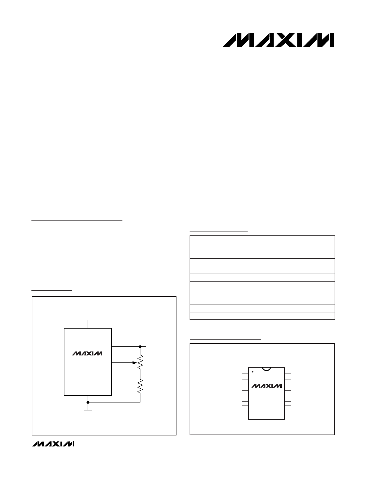
REFERENCE WITH TRIMMED OUTPUT
V
OUT
TRIM
MAX872
MAX874
Typical Operating Circuit
19-0005; Rev 2; 6/97
PART
MAX872CPA
MAX872CSA
MAX872C/D 0°C to +70°C
0°C to +70°C
0°C to +70°C
TEMP. RANGE PIN-PACKAGE
8 Plastic DIP
8 SO
Dice*
*
Dice are specified at +25°C only.
Pin Configuration
Ordering Information
MAX872EPA
MAX872ESA -40°C to +85°C
-40°C to +85°C 8 Plastic DIP
8 SO
MAX874CPA
MAX874CSA
MAX874C/D 0°C to +70°C
0°C to +70°C
0°C to +70°C 8 Plastic DIP
8 SO
Dice*
MAX874EPA
MAX874ESA -40°C to +85°C
-40°C to +85°C 8 Plastic DIP
8 SO
MAX872/MAX874
10µA, Low-Dropout,
Precision Voltage References
2 _______________________________________________________________________________________
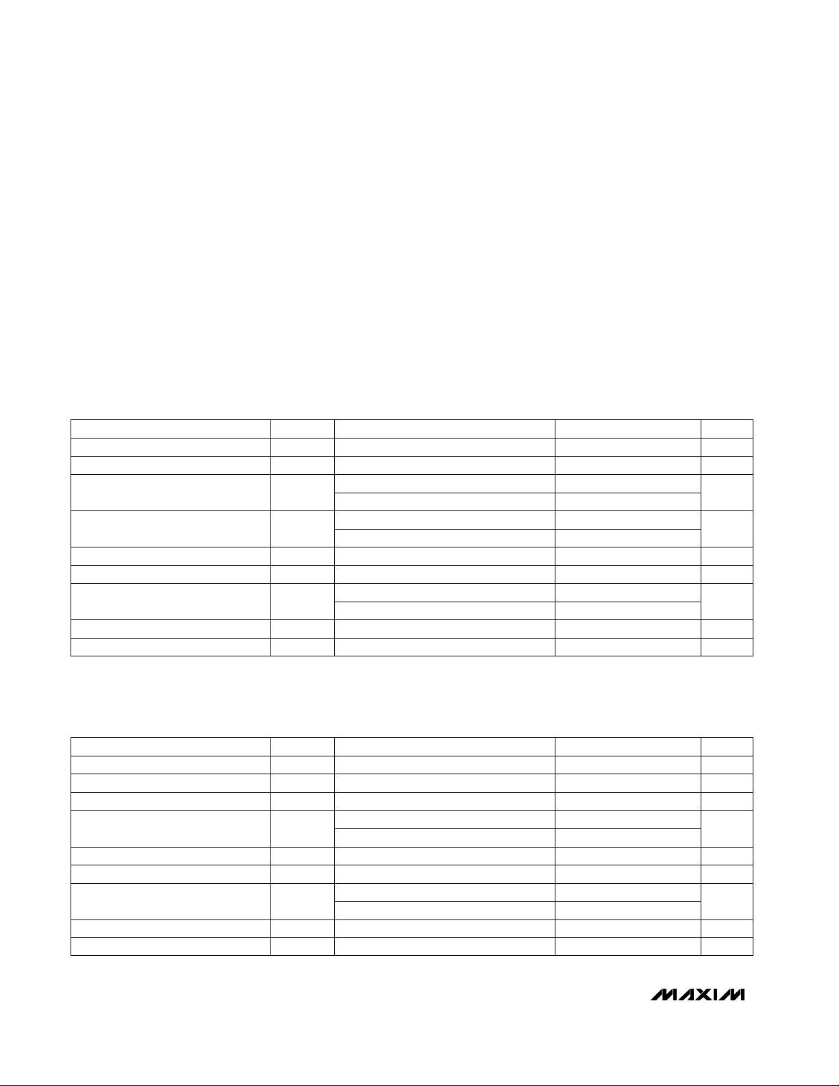
ABSOLUTE MAXIMUM RATINGS
ELECTRICAL CHARACTERISTICS—MAX872
(VIN= 2.7V, IL= 0mA, TA= +25°C, unless otherwise noted.)
Stresses beyond those listed under “Absolute Maximum Ratings” may cause permanent damage to the device. These are stress ratings only, and functional
operation of the device at these or any other conditions beyond those indicated in the operational sections of the specifications is not implied. Exposure to
absolute maximum rating conditions for extended periods may affect device reliability.
Supply Voltage.......................................................................24V
Output Short-Circuit Duration ..........Continuous to Either Supply
C
COMP
Input...........................................................-0.3V to V
OUT
TRIM Input ...................................................-0.3V to (VIN+ 0.3V)
TEMP Output ...............................................-0.3V to (V
IN
+ 0.3V)
Continuous Power Dissipation (T
A
= +70°C)
Plastic DIP (derate 9.09mW/°C above +70°C) .............727mW
SO (derate 5.88mW/°C above +70°C)..........................471mW
Operating Temperature Ranges
MAX87_C__ .........................................................0°C to +70°C
MAX87_E__ ......................................................-40°C to +85°C
Storage Temperature Range.............................-65°C to +150°C
Junction Temperature Range (T
j
)......................-65°C to +160°C
Lead Temperature (soldering, 10sec).............................+300°C
VIN= 4.5V to 20V
0.1Hz to 10Hz
V
OUT
short to V
IN
V
OUT
short to GND
VIN= 2.7V to 20V
VIN= 2.7V to 5.5V
Sourcing 0mA to 0.5mA
Sinking 0mA to -0.5mA
V
OUT
≥ V
OUT
+ 0.2V
CONDITIONS
mV+75/-20 +100/-25V
ADJ
V
OUT
Adjustment Range
412
µVp-p60e
n
V2.495 2.500 2.505V
OUT
Output Voltage
Output Voltage Noise
mV690V
TEMP
TEMP Voltage
mA
39
I
SC
Short-Circuit Output Current
615
µA/V0.35 0.55IQ/V
IN
Change in Supply Current vs. V
IN
µV/V
80 250
V
OUT/VIN
Line Regulation
0.2 0.5
mV/mA
412
V
OUT/IOUT
Load Regulation (Note 1)
µA6.5 10I
Q
Quiescent Supply Current
UNITSMIN TYP MAXSYMBOLPARAMETER
ELECTRICAL CHARACTERISTICS—MAX874
(VIN= 4.3V, IL= 0mA, TA= +25°C, unless otherwise noted.)
VIN= 4.3V to 20V
0.1Hz to 10Hz
V
OUT
short to V
IN
V
OUT
short to GND
VIN= 4.3V to 20V
Sourcing 0mA to 0.5mA
Sinking 0mA to -0.5mA
V
OUT
≥ V
OUT
+ 0.2V
CONDITIONS
mV±150 ±200V
ADJ
V
OUT
Adjustment Range
15 75
µVp-p90e
n
V4.088 4.096 4.104V
OUT
Output Voltage
Output Voltage Noise
mV690V
TEMP
TEMP Voltage
mA
525
I
SC
Short-Circuit Output Current
615
µA/V0.35 0.55IQ/V
IN
Change in Supply Current vs. V
IN
µV/VV
OUT/VIN
Line Regulation
0.15 0.9
mV/mA
615
V
OUT/IOUT
Load Regulation (Note 1)
µA6.5 10I
Q
Quiescent Supply Current
UNITSMIN TYP MAXSYMBOLPARAMETER
MAX872/MAX874
10µA, Low-Dropout,
Precision Voltage References
_______________________________________________________________________________________ 3
Note 1: If the load current exceeds 300µA, connect a minimum of 1000pF from V
OUT
to GND. Note that if a capacitor larger than
1000pF is used, a compensation capacitor of C
OUT
/100 must be connected from V
OUT
to COMP.
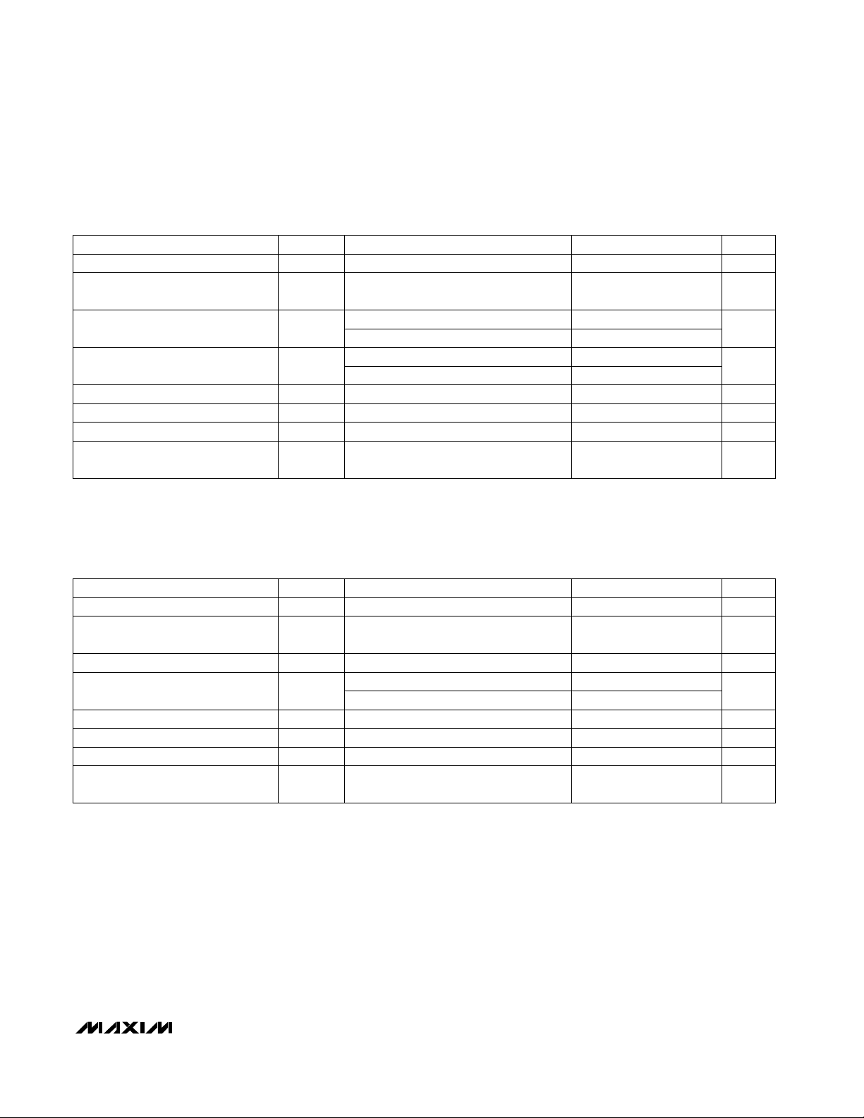
ELECTRICAL CHARACTERISTICS—MAX872C
(VIN= 2.7V, IL= 0mA, TA= 0°C to +70°C, unless otherwise noted.)
VIN= 4.5V to 20V
VIN= 2.7V to 20V
VIN= 2.7V to 5.5V
Sourcing 0mA to 0.4mA
Sinking 0mA to -0.4mA
CONDITIONS
20
ppm/°C20 40TCV
OUT
V2.4905 2.5095V
OUT
Output Voltage
Output Voltage Temperature
Coefficient
mV/°C2.3TCV
TEMP
TEMP Output Temperature
Coefficient
µA/V0.7IQ/V
IN
Change in Supply Current vs. V
IN
µV/V
300
V
OUT/VIN
Line Regulation
0.6
mV/mA
15
V
OUT/IOUT
Load Regulation (Note 1)
µA15I
Q
Quiescent Supply Current
UNITSMIN TYP MAXSYMBOLPARAMETER
VIN≥ V
OUT
+ 0.2V mV+75/-20V
ADJ
V
OUT
Adjustment Range
ELECTRICAL CHARACTERISTICS—MAX874C
(VIN= 4.3V, IL= 0mA, TA= 0°C to +70°C, unless otherwise noted.)
VIN≥ V
OUT
+ 0.2V mV±150
VIN= 4.3V to 20V
V
ADJ
V
OUT
Adjustment Range
VIN= 4.3V to 20V
Sourcing 0mA to 0.4mA
Sinking 0mA to -0.4mA
CONDITIONS
75
ppm/°C20 40TCV
OUT
V4.0805 4.1115V
OUT
Output Voltage
Output Voltage Temperature
Coefficient
mV/°C2.3TCV
TEMP
TEMP Output Temperature
Coefficient
µA/V0.7IQ/V
IN
Change in Supply Current vs. V
IN
µV/VV
OUT/VIN
Line Regulation
1.0
mV/mA
25
V
OUT/IOUT
Load Regulation (Note 1)
µA15I
Q
Quiescent Supply Current
UNITSMIN TYP MAXSYMBOLPARAMETER

MAX872/MAX874
10µA, Low-Dropout,
Precision Voltage References
4 _______________________________________________________________________________________
ELECTRICAL CHARACTERISTICS—MAX872E
(VIN= 2.7V, IL= 0mA, TA= -40°C to +85°C, unless otherwise noted.)
VIN≥ V
OUT
+ 0.2V mV+75/-20
VIN= 4.5V to 20V
V
ADJ
V
OUT
Adjustment Range
VIN= 2.7V to 20V
VIN= 2.7V to 5.5V
Sourcing 0mA to 0.30mA
Sinking 0mA to -0.30mA
CONDITIONS
20
ppm/°C20 40TCV
OUT
V2.488 2.512V
OUT
Output Voltage
Output Voltage Temperature
Coefficient
mV/°C2.3TCV
TEMP
TEMP Output Temperature
Coefficient
µA/V0.7IQ/V
IN
Change in Supply Current vs. V
IN
µV/V
300
V
OUT/VIN
Line Regulation
0.6
mV/mA
15
V
OUT/IOUT
Load Regulation
µA15I
Q
Quiescent Supply Current
UNITSMIN TYP MAXSYMBOLPARAMETER
ELECTRICAL CHARACTERISTICS—MAX874E
(VIN= 4.3V, IL= 0mA, TA= -40°C to +85°C, unless otherwise noted.)
VIN≥ V
OUT
+ 0.2V mV±150
VIN= 4.3V to 20V
V
ADJ
V
OUT
Adjustment Range
VIN= 4.3V to 20V
Sourcing 0mA to 0.30mA
Sinking 0mA to -0.30mA
CONDITIONS
75
ppm/°C20 40TCV
OUT
V4.077 4.115V
OUT
Output Voltage
Output Voltage Temperature
Coefficient
mV/°C2.3TCV
TEMP
TEMP Output Temperature
Coefficient
µA/V0.7IQ/V
IN
Change in Supply Current vs. V
IN
µV/VV
OUT/VIN
Line Regulation
1.0
mV/mA
25
V
OUT/IOUT
Load Regulation
µA15I
Q
Quiescent Supply Current
UNITSMIN TYP MAXSYMBOLPARAMETER

MAX872/MAX874
10µA, Low-Dropout,
Precision Voltage References
_______________________________________________________________________________________
5
0
50
150
100
200
250
100 150 200 250
DROPOUT VOLTAGE
vs. SOURCE CURRENT
MAX872/74-01
SOURCE CURRENT (µA)
DROPOUT VOLTAGE (mV)
TA = +85°C
TA = -40°C
TA = +25°C
0
10
5
15
20
0 2 4 6 8 10 12 14 16 18 20
SUPPLY CURRENT
vs. INPUT VOLTAGE
MAX872/74-02
INPUT VOLTAGE (V)
SUPPLY CURRENT (µA)
MAX874
MAX872
5
10
15
20
-50 -25 0 25 50 75 100
MAX872
SUPPLY CURRENT vs. TEMPERATURE
MAX872/74-03
TEMPERATURE (°C)
SUPPLY CURRENT (µA)
NO LOAD
VIN = 20V
VIN = 5V
VIN = 3V
VIN = 10V
5
15
10
20
25
-50 -25 0 25 50 75 100
MAX874
SUPPLY CURRENT vs. TEMPERATURE
MAX872/74-04
TEMPERATURE (°C)
SUPPLY CURRENT (µA)
VIN = 20V
VIN = 10V
VIN = 5V
0
2
1
3
4
-50 -25 0 25 50 75 100
MAX872
LOAD REGULATION vs. TEMPERATURE
MAX872/74-07
TEMPERATURE (°C)
LOAD REGULATION (mV/mA)
SINKING 0µA TO -500µA
SOURCING 0µA TO 500µA
2.495
2.498
2.500
2.503
2.505
2 6 10 164 8 14 1812 20
MAX872
OUTPUT VOLTAGE vs. INPUT VOLTAGE
MAX872/74-05
INPUT VOLTAGE (V)
V
OUT
(V)
4.090
4.094
4.092
4.096
4.098
4.100
4 8 12 16610141820
MAX874
OUTPUT VOLTAGE vs. INPUT VOLTAGE
MAX872/74-06
INPUT VOLTAGE (V)
V
OUT
(V)
0
3
2
1
4
5
-50 -25 0 25 50 75 100
MAX874
LOAD REGULATION vs. TEMPERATURE
MAX872/74-08
TEMPERATURE (°C)
LOAD REGULATION (mV/mA)
SINKING 0µA TO -500µA
SOURCING 0µA TO 500µA
2.498
0.01 1010.1
MAX872
OUTPUT VOLTAGE
vs. SOURCE CURRENT
2.501
2.500
2.502
2.499
MAX872/74-09
SOURCE CURRENT (mA)
V
OUT
(V)
Typical Operating Characteristics
(VIN= 3V (MAX872), VIN= 5V (MAX874), no load, TA = +25°C, unless otherwise noted.)

MAX872/MAX874
10µA, Low-Dropout,
Precision Voltage References
6 _______________________________________________________________________________________
Typical Operating Characteristics (continued)
(VIN= 3V (MAX872), VIN= 5V (MAX874), no load, TA = +25°C, unless otherwise noted.)
4.094
0.01 1010.1
MAX874
OUTPUT VOLTAGE
vs. SOURCE CURRENT
4.097
4.096
4.098
4.095
MAX872/74-10
SOURCE CURRENT (mA)
V
OUT
(V)
2.496
2.498
2.502
2.500
2.504
2.506
-50 0-25 25 50 75 100
MAX872
OUTPUT VOLTAGE vs. TEMPERATURE
MAX872/74-11
TEMPERATURE (°C)
V
OUT
(V)
4.090
4.092
4.096
4.094
4.098
4.100
-50 0-25 25 50 75 100
MAX874
OUTPUT VOLTAGE vs. TEMPERATURE
MAX872/74-12
TEMPERATURE (°C)
V
OUT
(V)
-20
-80
1 100 1k10 10k
POWER-SUPPLY REJECTION RATIO
vs. FREQUENCY
-60
MAX872/74-13
FREQUENCY (Hz)
PSRR (dB)
-40
NO LOAD
V
IN
= +3V TO +5V (MAX872)
V
IN
= +5V TO +7V (MAX874)
NO INPUT FILTER
INPUT FILTER
CIRCUIT IN FIGURE 2
MAX872
1Hz TO 100Hz NOISE
0.5
0.6
0.8
0.7
0.9
1.0
-50 0-25 25 50 75 100
TEMP OUTPUT
vs. TEMPERATURE
MAX872/74-14
TEMPERATURE (°C)
TEMP OUTPUT (V)
NO LOAD
2.0
0
1 100 1k10 10k
NOISE vs. FREQUENCY
0.5
MAX872/74-15
FREQUENCY (Hz)
NOISE (mVp-p)
1.5
1.0
MAX874
MAX872
NOISE IS FROM
0.01Hz TO FREQUENCY
INDICATED
MAX874
1Hz TO 100Hz NOISE

Applications Information
Trimming the Output Voltage
The MAX872/MAX874’s output voltage is trimmed for
0.2% tolerance at +25°C. If additional V
OUT
trimming is
desired, connect a potentiometer to TRIM, as shown in
Figures 1a and 1b. Adjusting V
OUT
away from its factory-trimmed voltage typically changes the output voltage
tempco by 7ppm/°C per 100mV.
Reducing Input Ripple with an Input Filter
The Power-Supply Rejection Ratio vs. Frequency graph
in the
Typical Operating Characteristics
shows ripple
rejection between 10Hz and 2kHz. As input RC filter
with a pole less than 10Hz, as shown in Figure 2, further attenuates input ripple with this band. The voltage
drop across the input resistor (due to supply and load
current) slightly increases the dropout voltage. The
increase is given by [(I
LOAD
+ I
SUPPLY
) • R].
Choosing the Output and
Compensation Capacitors
Connecting a capacitor between Void and GND
reduces load transients. If the load exceeds 300µA,
connect a minimum of 1000pF from V
OUT
to GND. The
type of capacitor is not critical. If the total load capacitance from V
OUT
to GND (C
LOAD
= output capacitor +
other capacitive load) is larger than 1000pF, connect a
compensation capacitor with a value of C
LOAD
/100
between COMP and V
OUT
.
MAX872/MAX874
10µA, Low-Dropout,
Precision Voltage References
_______________________________________________________________________________________ 7
Pin Description
Internal Connection. Make no connection
to this pin
I.C.1, 7
PIN FUNCTIONNAME
Input VoltageV
IN
2
GroundGND4
Temperature-Proportional Output
Voltage. Generates an output voltage
proportional to junction temperature.
TEMP3
Output Voltage Trim. Connect to the
center of a voltage divider for output
trimming. Otherwise make no
connection.
TRIM5
Compensation Input. Connect
C
LOAD
/100 capacitor from V
OUT
to
COMP to provide capacitive load
compensation.
COMP8
Reference OutputV
OUT
6
Figure 1a. Adjusting V
OUT
with the TRIM Input on the MAX872
GND
2M
1M
4M
TRIM RANGE: -200mV/+300mV
V
OUT
V
IN
TRIM
MAX874
5V
Figure 1b. Adjusting V
OUT
with the TRIM Input on the MAX874
V
3V
IN
V
OUT
MAX872
TRIM RANGE: -35mV/+80mV
TRIM
GND
1M
1.5M

MAX872/MAX874
10µA, Low-Dropout,
Precision Voltage References
Maxim cannot assume responsibility for use of any circuitry other than circuitry entirely embodied in a Maxim product. No circuit patent licenses are
implied. Maxim reserves the right to change the circuitry and specifications without notice at any time.
8
_____________________Maxim Integrated Products, 120 San Gabriel Drive, Sunnyvale, CA 94086 408-737-7600
© 1997 Maxim Integrated Products Printed USA is a registered trademark of Maxim Integrated Products.
TEMP Output
The TEMP output provides a voltage proportional to the
MAX872/MAX874 junction temperature. Since the
power dissipation of the MAX872/MAX874 is <100µW
typ, the junction temperature is within 0.5°C of the
ambient temperature. Although it goes unused in most
applications, the ambient temperature information
given by the TEMP output may be used to control LCD
contrast, or to provide ADC gain compensation or thermal out-of-range indication. TEMP must be buffered or
connected to a high-impedance input.
Operating Temperature
Window Comparator
In Figure 3, a window comparator monitors the TEMP
output and indicates if the temperature is out of the
nominal operating range. For the resistor values shown,
the circuit will indicate an out-of-range condition if the
ambient temperature should rise above +85°C or dip
below -40°C.
Start-Up
When the input voltage is below the factory-selected
output voltage, the MAX872/MAX874 can draw excessive supply current (hundreds of microamps). If the
source resistance is too high, the voltage drop across
the source resistance can prevent the input voltage to
the device from reaching the minimum dropout voltage.
Therefore, when using the MAX872/MAX874 in lowdropout applications, ensure that the power supply has
a low source resistance.
GND
0.047µF
4.7µF
COMP
150Ω
V
IN
V
OUT
MAX872
MAX874
3.0V (MAX872)
5.0V (MAX874)
100µF
Figure 2. Input Filter Reduces Input Ripple
GND
V+
V
OUT
170k (MAX872)
330k (MAX874)
27k
54k
V
IN
TEMP
MAX872
MAX874
1/2
MAX922
+5V
UNDER TEMP
-40°C TO +85°C OPERATING RANGE
OVER TEMP
REF OUT
1/4 74HC86
TEMP OUT OF RANGE
+5V
1/2
MAX922
Figure 3. Operating Temperature Range Window Comparator
___________________Chip Topography
GND
TEMP
V
IN
*N.C.
OUT
TRIM
0.110"
(2.794mm)
0.072"
(1.829mm)
*N.C.COMP
*MAKE NO CONNECTIONS TO THESE PADS
TRANSISTOR COUNT: 89
SUBSTRATE CONNECTED TO GND.
MAX872/MAX874
 Loading...