For free samples & the latest literature: http://www.maxim-ic.com, or phone 1-800-998-8800.
For small orders, phone 408-737-7600 ext. 3468.
_______________General Description
The MAX869L P-channel load switch features an accurate user-set current limit and low on-resistance. This
switch is designed to protect your power source from
shorts and surges by limiting current and preventing
the system supply from being pulled low. The input voltage range is 2.7V to 5.5V.
The MAX869L features a 2A, 45mΩ switch controlled
by a logic signal. Current-limit accuracy is ±21%, and
can be set from 400mA to 2.4A using a single resistor.
The device has a low 12µA quiescent supply current,
which reduces to 2µA max in shutdown. It features thermal-shutdown protection and a logic-signal output pin
(FAULT) that signals when there is an overcurrent or
overtemperature condition.
For other devices in this family, consult the
Selector
Guide
.
________________________Applications
Universal Serial Bus (USB)
Notebook Computers
Personal Communicators
Palmtop Computers
Hand-Held Instruments
Portable Medical Instruments
____________________________Features
♦ Very Small Footprint (16-pin QSOP is the same
size as an 8-pin SO)
♦ Low Resistance: 45mΩ at 3V
♦ ±21%-Accurate, User-Set Current Limit
♦ 12µA (typ) Quiescent Current
♦ 0.01µA (typ) Shutdown Current
♦ 0.04µA (typ) Leakage to Output when Switch
is Off
♦ 2.7V to 5.5V Input Range
♦ Thermal Shutdown
♦
FAULT Output
MAX869L
2A, Current-Limited, High-Side
P-Channel Switch with Thermal Shutdown
________________________________________________________________
Maxim Integrated Products
1
_____________________Selector Guide
19-1278; Rev 0; 8/97
PART
MAX869LC/D
MAX869LEEE -40°C to +85°C
0°C to +70°C
TEMP. RANGE PIN-PACKAGE
Dice*
16 QSOP
______________Ordering Information
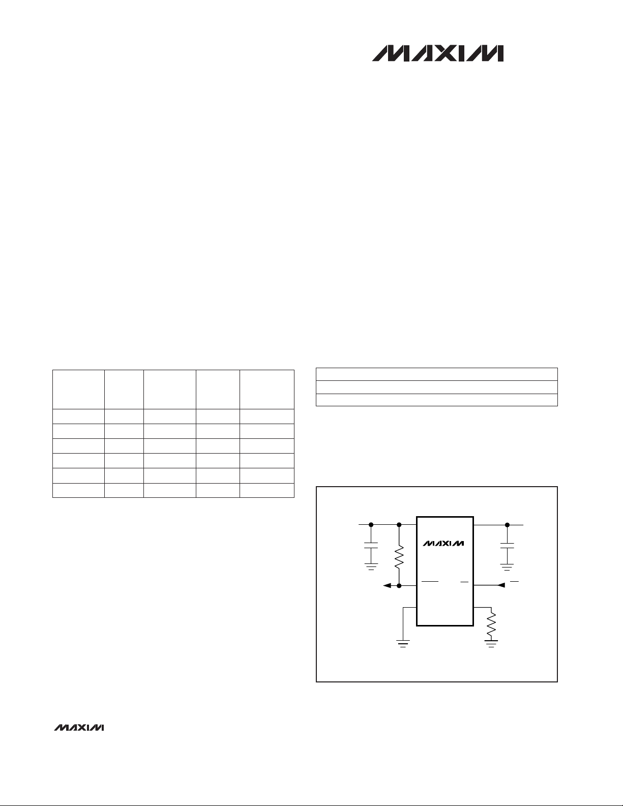
__________Typical Operating Circuit
*
Dice are specified at TA= +25°C.
Pin Configuration appears at end of data sheet.
300
MAX892L
PART
150
MAX891L
45
MAX869L
R
ON
AT 3V
(mΩ)
0.25
0.5
2
NOMINAL
CURRENT
(A)
Single
Single
Single
COUNT
8 µMAX
8 µMAX
16 QSOP
PACKAGE
0.5 8 SODual150
MAX894L
0.25 8 SODual300
MAX895L
1 Single 8 SO90
MAX890L
MAX869L
IN
FAULT
OUT
INPUT
2.7V TO 5.5V
1µF
*
0.1µF*
ON/OFF
R
SET
OUTPUT
UP TO 2A
100k
*FOR USB APPLICATIONS, C
IN
= 1µF, C
OUT
= 120µF
ON
SET
GND

MAX869L
2A, Current-Limited, High-Side
P-Channel Switch with Thermal Shutdown
2 _______________________________________________________________________________________
Note 1: Guaranteed by design. Derived from the I
SET
current ratio; current-limit amplifier and external set resistor accuracies.
Note 2: Tested with I
OUT
= 200mA and V
SET
raised until (VIN- V
OUT
) ≥ 0.8V.
Note 3: Specifications to -40°C are guaranteed by design, not production tested.
ABSOLUTE MAXIMUM RATINGS
ELECTRICAL CHARACTERISTICS
(VIN= 3V, TA= 0°C to +85°C, unless otherwise noted. Typical values are at TA= +25°C.)
Stresses beyond those listed under “Absolute Maximum Ratings” may cause permanent damage to the device. These are stress ratings only, and functional
operation of the device at these or any other conditions beyond those indicated in the operational sections of the specifications is not implied. Exposure to
absolute maximum rating conditions for extended periods may affect device reliability.
IN to GND ..................................................................-0.3V to 6V
ON, FAULT to GND ....................................................-0.3V to 6V
SET, OUT to GND ......................................-0.3V to (V
IN
+ 0.3V)
Maximum Continuous Switch Current .....................................3A
Continuous Power Dissipation (T
A
= +70°C)
QSOP (derate 8.3mW/°C above +70°C) .......................667mW
Operating Temperature Range
MAX869LEEE.....................................................-40°C to +85°C
Storage Temperature Range ........................... -65°C to +150°C
Lead Temperature (soldering, 10sec).............................+300°C
ON = IN, VIN= V
OUT
= 5.5V
VIN= 5V, I
OUT
= 500mA
VIN= 3V, I
OUT
= 500mA
VIN= 5V, ON = GND, I
OUT
= 0A
VIN= 5V, I
OUT
= 500mA
20% current overdrive, VCC= 5V
V
FAULT
= 5.5V, V
SET
= 1V
VIN= 2.7V to 3.6V
VIN= 2.7V to 5.5V
I
SINK
= 1mA, V
SET
= 1.4V
V
SET
= 1.24V, I
OUT
= 0A
I
OUT
= 1A, V
OUT
> 1.6V
ON = IN, VIN= 5.5V, V
OUT
= 0V
Rising edge, 1% hysteresis
VIN= 4.75V
VON= 5.5V
R
SET
= 1% tolerance (Note 1)
VIN= 4.5V to 5.5V
CONDITIONS
VIN= 3.0V
mΩ
45 90
µs2 10 30
On-Resistance
Turn-Off Time
µs
200
Turn-On Time
100 300
µs4Fast-Current-Loop Response Time
µs10Slow-Current-Loop Response Time
µA0.05 1
FAULT Logic Output High Leakage Current
V0.4
FAULT Logic Output Low Voltage
µA0.05 ±3I
SET
Bias Current
µA0.01 ±1
ON Input Leakage
V
2.4
ON Input High Voltage
µA0.01 2Off-Supply Current
µA12 20
V2.7 5.5Operating Voltage
Quiescent Current
2.0
V0.8
ON Input Low Voltage
A/A810 955 1100I
OUT
to I
SET
Current Ratio
µA0.04 30Off-Switch Current
V2.0 2.3 2.6Undervoltage Lockout
38 70
A0.40 2.4Nominal Current-Limit Set Range
UNITSMIN TYP MAXPARAMETER
V
SET
required to turn the switch off (Note 2) V1.178 1.240 1.302Current-Limit-Amplifier Threshold

MAX869L
2A, Current-Limited, High-Side
P-Channel Switch with Thermal Shutdown
_______________________________________________________________________________________ 3
Note 1: Guaranteed by design. Derived from the I
SET
current ratio; current-limit amplifier and external set resistor accuracies.
Note 2: Tested with I
OUT
= 200mA and V
SET
raised until (VIN- V
OUT
) ≥ 0.8V.
Note 3: Specifications to -40°C are guaranteed by design, not production tested.
ELECTRICAL CHARACTERISTICS
(VIN= 3V, TA= -40°C to +85°C, unless otherwise noted.) (Note 3)
VIN= 5V, I
OUT
= 500mA µs2 30
ON = IN, VIN= V
OUT
= 5.5V
VIN= 5V, I
OUT
= 500mA
Turn-Off Time
VIN= 5V, ON = GND, I
OUT
= 0A
I
SINK
= 1mA, V
SET
= 1V
I
OUT
= 1A, V
OUT
> 1.6V
ON = IN, VIN= 5.5V, V
OUT
= 0V
Rising edge, 1% hysteresis
VIN= 4.75V
R
SET
= 1% tolerance (Note 1)
CONDITIONS
VIN= 3.0V
mΩ
90
µs400
On-Resistance
Turn-On Time
V0.4
FAULT Logic Output Low Voltage
µA2.5Off-Supply Current
µA25
V2.9 5.5Operating Voltage
Quiescent Current
A/A765 1145I
OUT
to I
SET
Current Ratio
µA30Off-Switch Current
V2.0 2.85Undervoltage Lockout
70
A0.40 2.4Nominal Current-Limit Set Range
UNITSMIN TYP MAXPARAMETER
V
SET
required to turn the switch off (Note 2) V1.14 1.34Current-Limit-Amplifier Threshold
 Loading...