

For free samples & the latest literature: http://www.maxim-ic.com, or phone 1-800-998-8800.
For small orders, phone 408-737-7600 ext. 3468.
_______________General Description
The MAX869L P-channel load switch features an accurate user-set current limit and low on-resistance. This
switch is designed to protect your power source from
shorts and surges by limiting current and preventing
the system supply from being pulled low. The input voltage range is 2.7V to 5.5V.
The MAX869L features a 2A, 45mΩ switch controlled
by a logic signal. Current-limit accuracy is ±21%, and
can be set from 400mA to 2.4A using a single resistor.
The device has a low 12µA quiescent supply current,
which reduces to 2µA max in shutdown. It features thermal-shutdown protection and a logic-signal output pin
(FAULT) that signals when there is an overcurrent or
overtemperature condition.
For other devices in this family, consult the
Selector
Guide
.
________________________Applications
Universal Serial Bus (USB)
Notebook Computers
Personal Communicators
Palmtop Computers
Hand-Held Instruments
Portable Medical Instruments
____________________________Features
♦ Very Small Footprint (16-pin QSOP is the same
size as an 8-pin SO)
♦ Low Resistance: 45mΩ at 3V
♦ ±21%-Accurate, User-Set Current Limit
♦ 12µA (typ) Quiescent Current
♦ 0.01µA (typ) Shutdown Current
♦ 0.04µA (typ) Leakage to Output when Switch
is Off
♦ 2.7V to 5.5V Input Range
♦ Thermal Shutdown
♦
FAULT Output
MAX869L
2A, Current-Limited, High-Side
P-Channel Switch with Thermal Shutdown
________________________________________________________________
Maxim Integrated Products
1
_____________________Selector Guide
19-1278; Rev 0; 8/97
PART
MAX869LC/D
MAX869LEEE -40°C to +85°C
0°C to +70°C
TEMP. RANGE PIN-PACKAGE
Dice*
16 QSOP
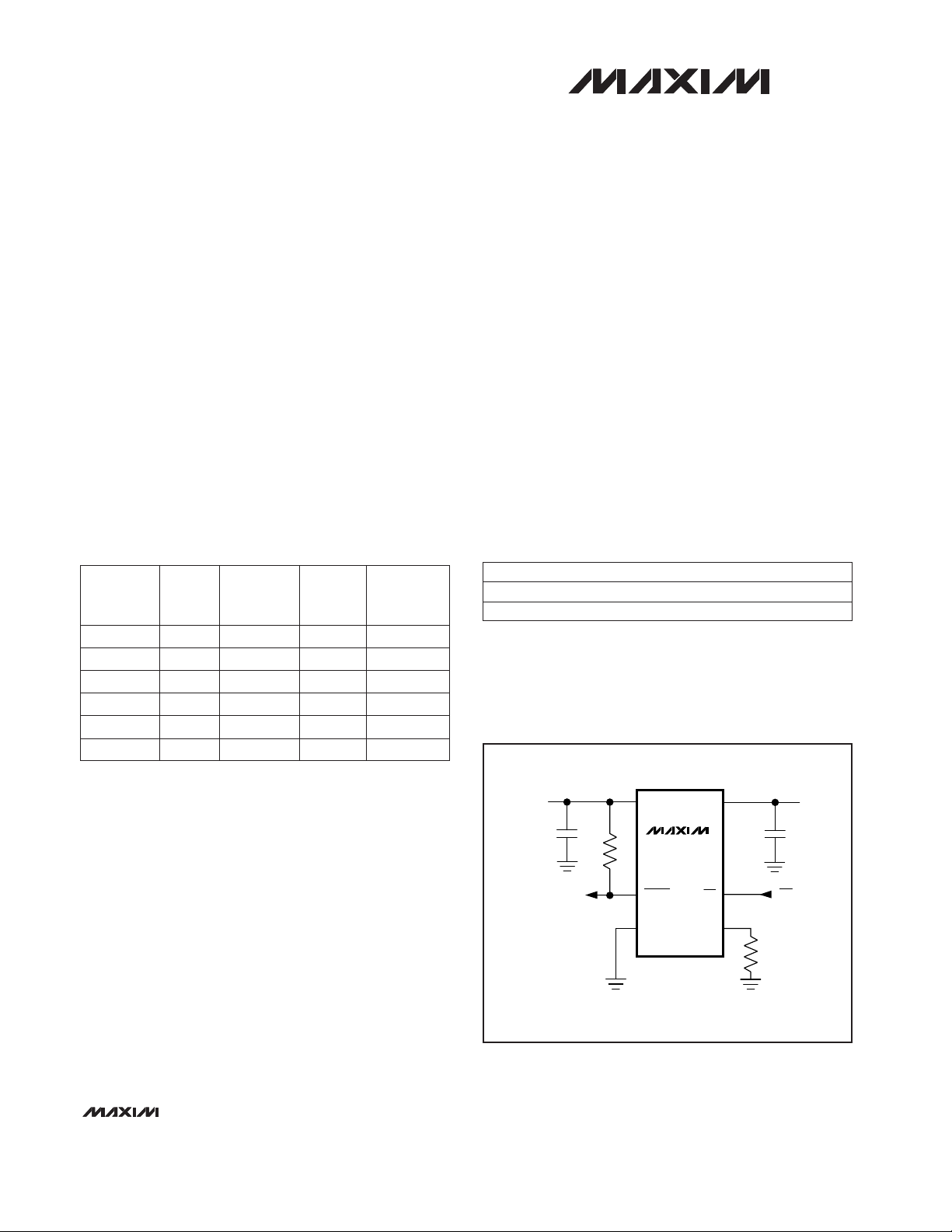
______________Ordering Information
__________Typical Operating Circuit
*
Dice are specified at TA= +25°C.
Pin Configuration appears at end of data sheet.
300
MAX892L
PART
150
MAX891L
45
MAX869L
R
ON
AT 3V
(mΩ)
0.25
0.5
2
NOMINAL
CURRENT
(A)
Single
Single
Single
COUNT
8 µMAX
8 µMAX
16 QSOP
PACKAGE
0.5 8 SODual150
MAX894L
0.25 8 SODual300
MAX895L
1 Single 8 SO90
MAX890L
MAX869L
IN
FAULT
OUT
INPUT
2.7V TO 5.5V
1µF
*
0.1µF*
ON/OFF
R
SET
OUTPUT
UP TO 2A
100k
*FOR USB APPLICATIONS, C
IN
= 1µF, C
OUT
= 120µF
ON
SET
GND
MAX869L
2A, Current-Limited, High-Side
P-Channel Switch with Thermal Shutdown
2 _______________________________________________________________________________________
Note 1: Guaranteed by design. Derived from the I
SET
current ratio; current-limit amplifier and external set resistor accuracies.
Note 2: Tested with I
OUT
= 200mA and V
SET
raised until (VIN- V
OUT
) ≥ 0.8V.
Note 3: Specifications to -40°C are guaranteed by design, not production tested.
ABSOLUTE MAXIMUM RATINGS
ELECTRICAL CHARACTERISTICS
(VIN= 3V, TA= 0°C to +85°C, unless otherwise noted. Typical values are at TA= +25°C.)
Stresses beyond those listed under “Absolute Maximum Ratings” may cause permanent damage to the device. These are stress ratings only, and functional
operation of the device at these or any other conditions beyond those indicated in the operational sections of the specifications is not implied. Exposure to
absolute maximum rating conditions for extended periods may affect device reliability.
IN to GND ..................................................................-0.3V to 6V
ON, FAULT to GND ....................................................-0.3V to 6V
SET, OUT to GND ......................................-0.3V to (V
IN
+ 0.3V)
Maximum Continuous Switch Current .....................................3A
Continuous Power Dissipation (T
A
= +70°C)
QSOP (derate 8.3mW/°C above +70°C) .......................667mW
Operating Temperature Range
MAX869LEEE.....................................................-40°C to +85°C
Storage Temperature Range ........................... -65°C to +150°C
Lead Temperature (soldering, 10sec).............................+300°C
ON = IN, VIN= V
OUT
= 5.5V
VIN= 5V, I
OUT
= 500mA
VIN= 3V, I
OUT
= 500mA
VIN= 5V, ON = GND, I
OUT
= 0A
VIN= 5V, I
OUT
= 500mA
20% current overdrive, VCC= 5V
V
FAULT
= 5.5V, V
SET
= 1V
VIN= 2.7V to 3.6V
VIN= 2.7V to 5.5V
I
SINK
= 1mA, V
SET
= 1.4V
V
SET
= 1.24V, I
OUT
= 0A
I
OUT
= 1A, V
OUT
> 1.6V
ON = IN, VIN= 5.5V, V
OUT
= 0V
Rising edge, 1% hysteresis
VIN= 4.75V
VON= 5.5V
R
SET
= 1% tolerance (Note 1)
VIN= 4.5V to 5.5V
CONDITIONS
VIN= 3.0V
mΩ
45 90
µs2 10 30
On-Resistance
Turn-Off Time
µs
200
Turn-On Time
100 300
µs4Fast-Current-Loop Response Time
µs10Slow-Current-Loop Response Time
µA0.05 1
FAULT Logic Output High Leakage Current
V0.4
FAULT Logic Output Low Voltage
µA0.05 ±3I
SET
Bias Current
µA0.01 ±1
ON Input Leakage
V
2.4
ON Input High Voltage
µA0.01 2Off-Supply Current
µA12 20
V2.7 5.5Operating Voltage
Quiescent Current
2.0
V0.8
ON Input Low Voltage
A/A810 955 1100I
OUT
to I
SET
Current Ratio
µA0.04 30Off-Switch Current
V2.0 2.3 2.6Undervoltage Lockout
38 70
A0.40 2.4Nominal Current-Limit Set Range
UNITSMIN TYP MAXPARAMETER
V
SET
required to turn the switch off (Note 2) V1.178 1.240 1.302Current-Limit-Amplifier Threshold
MAX869L
2A, Current-Limited, High-Side
P-Channel Switch with Thermal Shutdown
_______________________________________________________________________________________ 3
Note 1: Guaranteed by design. Derived from the I
SET
current ratio; current-limit amplifier and external set resistor accuracies.
Note 2: Tested with I
OUT
= 200mA and V
SET
raised until (VIN- V
OUT
) ≥ 0.8V.
Note 3: Specifications to -40°C are guaranteed by design, not production tested.
ELECTRICAL CHARACTERISTICS
(VIN= 3V, TA= -40°C to +85°C, unless otherwise noted.) (Note 3)
VIN= 5V, I
OUT
= 500mA µs2 30
ON = IN, VIN= V
OUT
= 5.5V
VIN= 5V, I
OUT
= 500mA
Turn-Off Time
VIN= 5V, ON = GND, I
OUT
= 0A
I
SINK
= 1mA, V
SET
= 1V
I
OUT
= 1A, V
OUT
> 1.6V
ON = IN, VIN= 5.5V, V
OUT
= 0V
Rising edge, 1% hysteresis
VIN= 4.75V
R
SET
= 1% tolerance (Note 1)
CONDITIONS
VIN= 3.0V
mΩ
90
µs400
On-Resistance
Turn-On Time
V0.4
FAULT Logic Output Low Voltage
µA2.5Off-Supply Current
µA25
V2.9 5.5Operating Voltage
Quiescent Current
A/A765 1145I
OUT
to I
SET
Current Ratio
µA30Off-Switch Current
V2.0 2.85Undervoltage Lockout
70
A0.40 2.4Nominal Current-Limit Set Range
UNITSMIN TYP MAXPARAMETER
V
SET
required to turn the switch off (Note 2) V1.14 1.34Current-Limit-Amplifier Threshold

MAX869L
2A, Current-Limited, High-Side
P-Channel Switch with Thermal Shutdown
4 _______________________________________________________________________________________
__________________________________________Typical Operating Characteristics
(TA = +25°C, unless otherwise noted.)
0
2
4
6
8
10
12
14
QUIESCENT CURRENT
vs. INPUT VOLTAGE
MAX869-01
INPUT VOLTAGE (V)
QUIESCENT CURRENT (µA)
0 1 2 3 4 5 6
ON = GND
I
OUT
= 0A
8
-40 -20 4020 100
QUIESCENT CURRENT
vs. TEMPERATURE
MAX869-02
TEMPERATURE (°C)
QUIESCENT CURRENT (µA)
0 60 80
13
11
9
14
12
10
V
IN
= 3V
V
IN
= 5V
0
4
2
6
8
10
14
12
16
18
20
-40 -20 4020 100
OFF-SUPPLY CURRENT
vs. TEMPERATURE
MAX869-03
TEMPERATURE (°C)
OFF-SUPPLY CURRENT (nA)
0 60 80
VIN = V
OUT
= 5.5V
IN = ON
0
100
200
300
500
400
600
700
-40 -20 4020 100
OFF-SWITCH CURRENT
vs. TEMPERATURE
MAX869-04
TEMPERATURE (°C)
OFF-SWITCH CURRENT (nA)
0 60 80
VIN = VON = 5.5V
OUT = GND
0
0.2
0.4
0.6
0.8
1.0
1.2
NORMALIZED OUTPUT CURRENT
vs. OUTPUT VOLTAGE
MAX869-06A
OUTPUT VOLTAGE (V)
NORMALIZED OUTPUT CURRENT
0 1 2 3 4 5 6
I
LIMIT
V
IN
= 5V
0.6
-40 -20 4020 100
NORMALIZED ON-RESISTANCE
vs. TEMPERATURE
0.9
0.8
MAX890-05
TEMPERATURE (°C)
NORMALIZED R
ON
0 60 80
1.3
1.1
0.7
1.4
1.2
1.0
I
OUT
= 1/2I
LIMIT
0
0 0.4 1.61.2 2.8
I
OUT/ISET
RATIO
vs. SWITCH CURRENT
400
MAX890-06
I
SWITCH
(A)
I
OUT
/I
SET
RATIO
0.8 2.0 2.4
1200
800
200
1400
1000
600
260
0
TURN-ON TIME
vs. TEMPERATURE
80
60
220
MAX869-07
TEMPERATURE (°C)
t
ON
(µs)
160
120
240
40
20
200
180
140
100
C
IN
= 100µF
C
OUT
= 0.1µF
I
LOAD
= I
LIMIT
V
IN
= 3V
V
IN
= 5V
-40 -20 4020 1000 60 80
0
TURN-OFF TIME
vs. TEMPERATURE
4
12
MAX869-08
TEMPERATURE (°C)
t
OFF
(µs)
8
6
2
10
V
IN
= 3V
V
IN
= 5V
-40 -20 4020 1000 60 80
C
IN
= 100µF
C
OUT
= 0.1µF
I
LOAD
= I
LIMIT

MAX869L
2A, Current-Limited, High-Side
P-Channel Switch with Thermal Shutdown
_______________________________________________________________________________________
5
____________________________Typical Operating Characteristics (continued)
(TA = +25°C, unless otherwise noted.)
CIN = 100µF, C
OUT
= 0.1µF
A: V
FAULT
, 5V/div
B: V
OUT
, 5V/div
FAST CURRENT-LIMIT RESPONSE
A
B
C
D
0V
0A
0V
0V
2µs/div
C: I
OUT
, 5A/div
D: V
IN
, 5V/div
MA869-09
CIN = 100µF, C
OUT
= 0.1µF
A: V
FAULT
, 5V/div
B: V
OUT
, 5V/div
SLOW CURRENT-LIMIT RESPONSE
A
B
C
D
0V
0A
0V
0V
4µs/div
C: I
OUT
, 5A/div
D: V
IN
, 5V/div
MA869-10
VIN = 5V
A: I
OUT
= 0mA TO 1A, 0.5A/div
B: V
OUT
RIPPLE, 200mV/div, AC COUPLED
LOAD-TRANSIENT RESPONSE
A
B
0V
0A
10ms/div
MA869-11
CIN = 100µF, C
OUT
= 0.1µF, VIN = 5V, I
OUT
= 1A
A: V
ON
, 5V/div
B: V
OUT
, 2V/div
SWITCH TURN-OFF TIME
A
B
C
D
0V
0V
0V
0A
2µs/div
C: I
OUT
, 0.5A/div
D: V
FAULT
, 2V/div
MA869-13
CIN = 100µF, C
OUT
= 0.1µF, VIN = 5V, I
OUT
= 1A
A: V
ON
, 5V/div
B: V
OUT
, 2V/div
SWITCH TURN-ON TIME
A
B
C
D
0V
0V
0V
0A
20µs/div
C: I
OUT
, 0.5A/div
D: V
FAULT
, 2V/div
MA869-12

_______________Detailed Description
The MAX869L P-channel MOSFET power switch limits
output current to a programmed level. When the output
current passes through the main switch, a smaller current also passes through the replica switch (I
OUT
/ 955)
and through R
SET
(Figure 1). When the voltage on R
SET
exceeds the trip voltage of 1.24V, the current-limit error
amplifier regulates the output current to the programmed current limit, I
LIMIT
(400mA to 2.4A).
This switch is not bidirectional; therefore, the input voltage must be higher than the output voltage.
Setting the Current Limit
The MAX869L features internal current-limiting circuitry
with a maximum programmable value (I
MAX
) of 2.4A.
For best performance, set the current limit (I
LIMIT
)
between 0.2 I
MAX
≤ I
LIMIT
≤ I
MAX
. This current limit
remains in effect throughout the input supply-voltage
range.
Program the current limit with a resistor (R
SET
) from
SET to ground (Figure 2) as follows:
I
SET
= I
LIMIT
/ 955
R
SET
= 1.24V / I
SET
= 1,184 / I
LIMIT
where I
LIMIT
is the desired current limit.
MAX869L
2A, Current-Limited, High-Side
P-Channel Switch with Thermal Shutdown
6 _______________________________________________________________________________________
VIN = 5V, I
OUT
= 1A, CIN = 1µF, C
OUT
= 120µF
A: V
ON
, 5V/div
B: V
OUT
, 2V/div
*REFER TO
TYPICAL OPERATING CIRCUIT
USB* CIRCUIT OUTPUT RISE TIME
A
B
C
D
0V
0V
0V
0A
500µs/div
C: I
OUT
, 0.5A/div
D: V
FAULT
, 2V/div
MA869-14
____________________________Typical Operating Characteristics (continued)
(TA = +25°C, unless otherwise noted.)
USB* CIRCUIT OUTPUT FALL TIME
A
B
C
D
0V
0V
0V
0A
500µs/div
V
IN
= 5V, I
OUT
= 1A, CIN = 1µF, C
OUT
= 120µF
A: V
ON
, 5V/div
B: V
OUT
, 2V/div
C: I
OUT
, 0.5A/div
D: V
FAULT
, 2V/div
MA869-15
_____________________Pin Description
PIN
Input, P-channel MOSFET source.
Bypass IN with a 1µF capacitor to
ground.
IN
1, 4, 5,
12, 13, 16
FUNCTIONNAME
Switch output. P-channel MOSFET
drain. Bypass OUT with a 0.1µF
capacitor to GND.
OUT
2, 3, 6,
11, 14, 15
GroundGND8
Active-Low Switch-On Input. A logic
low turns the switch on.
ON
7
Fault-Indicator Output. This opendrain output goes low when in current limit or when the die temperature
exceeds +135°C. FAULT remains low
for Turn-On Time + 50µs during startup.
FAULT
10
Set Current-Limit Input. A resistor
from SET to ground sets the current
limit for the switch. R
SET
= 1,184 /
I
LIMIT
, where I
LIMIT
is the desired cur-
rent limit in amperes.
SET9

Short-Circuit Protection
The MAX869L is a short-circuit-protected switch. In the
event of an output short circuit (V
OUT
≤ 1.6V typical),
the current through the switch is limited by the internal
current-limiting error amplifier to 1.4 x I
LIMIT
. When the
short-circuit condition is removed, the current-limit
amplifier sets the current limit back to I
LIMIT
.
For a high ∆VDS/∆t during an output short-circuit condition, the switch turns off and disconnects the input supply
from the output. The current-limiting amplifier then slowly turns the switch on with the output current limited to
1.4 x I
LIMIT
. When the short-circuit condition is
removed, the current limit is set back to I
LIMIT
. Refer to the
Fast Current-Limit Response and Slow Current-Limit
Response graphs in the
Typical Operating Characteristics
.
Thermal Shutdown
The MAX869L features thermal shutdown. The switch
turns off when the junction temperature exceeds 135°C.
Once the device cools by 10°C, the switch turns back
on. If the fault condition is not removed, the switch
cycles on and off, resulting in a pulsed output.
Fault Indicator
The MAX869L provides a fault output (FAULT). This
open-drain output goes low when in current limit or
when the die temperature exceeds 135°C. A 100kΩ
pull-up resistor from FAULT to IN provides a logiccontrol signal.
__________Applications Information
Input Capacitor
To limit the input voltage drop during momentary output
short-circuit conditions, connect a capacitor from IN to
GND. A 1µF ceramic capacitor is adequate for most
applications; however, higher capacitor values further
reduce the voltage drop at the input.
Output Capacitor
Connect a 0.1µF capacitor from OUT to GND to prevent
inductive parasitics from pulling OUT below GND during turn-off. USB applications require C
OUT
to be at
least 120µF. This larger output capacitance slows the
output rise and fall times, as shown in the
Typical
Operating Characteristics
, but does not adversely
affect the MAX869L’s turn-off response time.
Layout and Thermal-Dissipation
Considerations
To take full advantage of the switch-response time to
output short-circuit conditions, it is very important to
keep all traces as short as possible to reduce the effect
of undesirable parasitic inductance. Place input and
output capacitors as close as possible to the device
(less than 5mm).
MAX869L
2A, Current-Limited, High-Side
P-Channel Switch with Thermal Shutdown
_______________________________________________________________________________________ 7
MAX869L
P
P
P
R
SET
SET
OUT
GND
1.24V
N
FAULT
ON
ON
CURRENT-LIMIT
AMPLIFIER
REPLICA
AMPLIFIER
ON
HOT
IN
CONTROL
CIRCUITRY
Figure 1. Functional Diagram
MAX869L
SET
R
SET
GND
Figure 2. Setting the Current Limit

MAX869L
2A, Current-Limited, High-Side
P-Channel Switch with Thermal Shutdown
Maxim cannot assume responsibility for use of any circuitry other than circuitry entirely embodied in a Maxim product. No circuit patent licenses are
implied. Maxim reserves the right to change the circuitry and specifications without notice at any time.
8
_____________________Maxim Integrated Products, 120 San Gabriel Drive, Sunnyvale, CA 94086 408-737-7600
© 1997 Maxim Integrated Products Printed USA is a registered trademark of Maxim Integrated Products.
Under normal operating conditions, the package can
dissipate and channel heat away. Calculate the maximum power as follows:
P = I
2
LIMIT
x R
ON
where RONis the on-resistance of the switch.
When the output is short circuited, the voltage drop
across the switch equals the input supply. Hence, the
power dissipated across the switch increases, as does
the die temperature. If the fault condition is not
removed, the thermal-overload-protection circuitry turns
the switch off until the die temperature falls by 10°C. A
ground plane in contact with the device helps dissipate
additional heat.
16
15
14
13
12
11
10
9
1
2
3
4
5
6
7
8
IN IN
OUT
OUT
IN
IN
OUT
FAULT
SET
TOP VIEW
MAX869L
QSOP
OUT
OUT
OUT
IN
IN
ON
GND
__________________Pin Configuration
___________________Chip Information
TRANSISTOR COUNT: 433
SUBSTRATE CONNECTED TO GND
 Loading...