

Page 1
MAX8662/MAX8663
Power-Management ICs for
Single-Cell, Li+ Battery-Operated Devices
________________________________________________________________
Maxim Integrated Products
1
Ordering Information
19-0732; Rev 0; 2/07
For pricing, delivery, and ordering information, please contact Maxim/Dallas Direct! at
1-888-629-4642, or visit Maxim’s website at www.maxim-ic.com.
♦
♦
♦
♦
♦
General Description
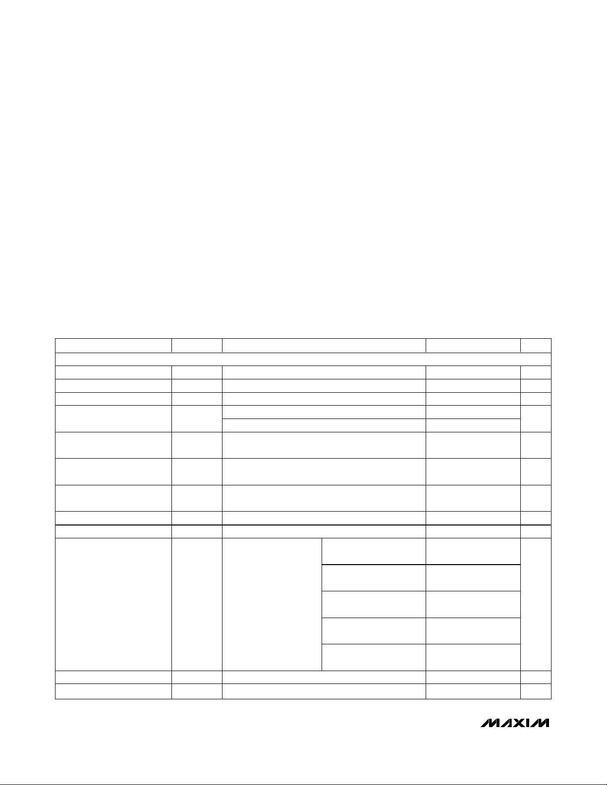
The MAX8662/MAX8663 power-management ICs
(PMICs) are efficient, compact devices suitable for
smart cellular phones, PDAs, Internet appliances, and
other portable devices. They integrate two synchronous
buck regulators, a boost regulator driving two to seven
white LEDs, four low-dropout linear regulators (LDOs),
and a linear charger for a single-cell Li-ion (Li+) battery.
Maxim’s Smart Power Selector™ (SPS) safely distributes power between an external power source (AC
adapter, auto adapter, or USB source), battery, and the
system load. When system load peaks exceed the
external source capability, the battery supplies supplemental current. When system load requirements are
small, residual power from the external power source
charges the battery. A thermal-limiting circuit limits battery-charge rate and external power-source current to
prevent overheating. The PMIC also allows the system
to operate with no battery or a discharged battery.
The MAX8662 is available in a 6mm x 6mm, 48-pin thin
QFN package, while the MAX8663, without the LED driver,
is available in a 5mm x 5mm, 40-pin thin QFN package.
Features
Applications
+
Denotes a lead-free package.
*
EP = Exposed paddle.
PART
TEMP
PIN-PACKAGE
PKG
CODE
MAX8662ETM+
-40°C to
48 Thin QFN-EP*
T4866-1
MAX8663ETL+
-40°C to
40 Thin QFN-EP*
T4055-1
Two 95%-Efficient 1MHz Buck Regulators
Main Regulator: 0.98V to V
IN
at 1200mA
Core Regulator: 0.98V to V
IN
at 900mA
1MHz Boost WLED Driver
Drives Up to 7 White LEDs at 30mA (max)
PWM and Analog Dimming Control
Four Low-Dropout Linear Regulators
1.7V to 5.5V Input Range
15µA Quiescent Current
Single-Cell Li+ Charger
Adapter or USB Input
Thermal-Overload Protection
Smart Power Selector (SPS)
AC Adapter/USB or Battery Source
Charger-Current and System-Load Sharing
Smart Phones and PDAs
MP3 and Portable Media Players
Palmtop and Wireless Handhelds
TOP VIEW
MAX8662
THIN QFN
(6mm x 6mm)
13
14
15
16
17
18
19
20
21
22
23
24
THM
ISET
CT
REF
GND
OUT4
IN45
OUT5
EN4
EN5
PWM
FB1
48
47
46
45
44
43
42
41
40
39
38
37
1
2
345678910
11
12
POK
PSET
SL2
SL1
VL
OUT7
IN67
OUT6
PG3
LX3
EN7
EN6
CEN
CHG
BRT
BAT2
BAT1
SYS2
SYS1
DC2
DC1
EN3
PEN2
PEN1
36
35
34 33 32 31 30 29 28 27
26
25
EN1
PG1
LX1
PV1
OVP
CS
CC3
FB2
PV2
LX2
PG2
EN2
Pin Configurations
OUT1
0.98V TO V
IN
/ 1.2A
OUT2
0.98V TO V
IN
/ 0.9A
OUT3
30mA
WLED
DC SYS
OUT7
EN1
500mA
150mA
300mA
150mA
Li+
BATTERY
DC/USB
INPUT
TO SYSTEM
POWER
BAT
LX1
LX2
LX3
(MAX8662 ONLY)
OUT6
OUT5
OUT4
CS
TO SYS
EN2
EN3
EN4
EN5
EN6
EN7
PWR OK
CHARGE
STATUS
CHARGE
ENABLE
SL1
SL2
OUT4–OUT7
VOLTAGE
SELECT
MAX8662
MAX8663
POK
CHG
CEN
Typical Operating Circuit
Smart Power Selector is a trademark of Maxim Integrated
Products, Inc.
Pin Configurations continued at end of data sheet.
EVALUATION KIT
AVAILABLE
RANGE
+85°C
+85°C
6mm x 6mm x 0.8mm
5mm x 5mm x 0.8mm
Page 2
MAX8662/MAX8663
Power-Management ICs for
Single-Cell, Li+ Battery-Operated Devices
2 _______________________________________________________________________________________
ABSOLUTE MAXIMUM RATINGS
ELECTRICAL CHARACTERISTICS (Input Limiter and Battery Charger)
(VDC= 5V, V
BAT
= 4V, V
CEN
= 0V, V
PEN_
= 5V, R
PSET
= 3kΩ, R
ISET
= 3.15kΩ, CCT= 0.068µF, TA= -40°C to +85°C, unless otherwise
noted.) (Note 1)
Stresses beyond those listed under “Absolute Maximum Ratings” may cause permanent damage to the device. These are stress ratings only, and functional
operation of the device at these or any other conditions beyond those indicated in the operational sections of the specifications is not implied. Exposure to
absolute maximum rating conditions for extended periods may affect device reliability.
LX3 to GND ............................................................-0.3V to +33V
DC_ to GND..............................................................-0.3V to +9V
BAT_ CEN, CHG, EN_, PEN_, POK, PV_, PWM,
SYS_, LX1, CS, LX2 to GND .................................-0.3V to +6V
VL to GND ................................................................-0.3V to +4V
BRT, CC3, FB_, IN45, IN67, OVP, REF,
SL_ to GND ...........................................-0.3V to (V
S
YS
+ 0.3V)
CT, ISET, PSET, THM to GND .....................-0.3V to (V
VL
+ 0.3V)
OUT4, OUT5 to GND................................-0.3V to (V
IN45
+ 0.3V)
OUT6, OUT7 to GND................................-0.3V to (V
IN67
+ 0.3V)
PG_ to GND...........................................................-0.3V to +0.3V
BAT1 + BAT2 Continuous Current ...........................................3A
SYS1 + SYS2 Continuous Current (2 pins) ..............................3A
LX_ Continuous Current ........................................................1.5A
Continuous Power Dissipation (T
A
= +70°C)
40-Pin 5mm x 5mm Thin QFN
(derate 35.7mW/°C above +70°C)
(multilayer board) .......................................................2857mW
48-Pin 6mm x 6mm Thin QFN
(derate 37mW/°C above +70°C) (multilayer board)...2963mW
Operating Temperature Range ..........................-40°C to +85°C
Junction Temperature Range ............................-40°C to +125°C
Storage Temperature Range .............................-65°C to +150°C
Lead Temperature (soldering, 10s) .................................+300°C
PARAMETER
CONDITIONS
UNITS
INPUT LIMITER
DC Operating Range V
DC
(Note 2)
V
V
DC_L
VDC rising, 500mV hysteresis
V
DC Overvoltage Threshold V
DC_H
VDC rising, 100mV hysteresis
V
I
SYS = IBAT =
0mA, V
CEN =
0V
DC Supply Current
I
SYS = IBAT =
0mA, V
CEN =
5V
mA
DC Shutdown Current
V
DC
= 5V, V
CEN =
5V, V
PEN1
= V
PEN2 =
0V (USB
suspend mode)
µA
DC-to-SYS Dropout
On-Resistance
V
DC
= 5V, I
SYS =
400mA, V
CEN =
5V
Ω
DC-to-BAT Dropout
Threshold
When V
SYS
regulation and charging stops, V
DC
falling, 150mV hysteresis
50 85
mV
VL Voltage V
VL
I
VL =
0 to 10mA
V
SYS Regulation Voltage
VDC = 5.8V, I
SYS =
1mA, V
CEN =
5V
V
R
PSET =
1.5kΩ
R
PSET
= 3kΩ
R
PSET
= 6kΩ
(500mA USB mode)
DC Input Current Limit I
DC_LIM
VDC = 5V, V
SYS
= 4.0V
V
PEN1
= V
PEN2 =
0V
(100mA USB mode)
90
mA
PSET Resistance Range R
PSET
Guaranteed by SYS current limit
kΩ
Inp ut Li m i ter S oft- S tar t Ti m e
Current-limit ramp time
ms
DC Undervoltage Threshold
SYMBOL
R
DC_SYS
V
DR_DC_BAT
V
SYS_REG
T
S S _ D C _S Y S
MIN TYP MAX
4.1 8.0
3.9 4.0 4.1
6.6 6.9 7.2
1.5
0.9
110 180
0.1 0.2
20
V
PEN1 =
V
PEN1 =
V
PEN1 =
V
PEN1 =
5V, V
5V, V
5V, V
0V, V
PEN2
PEN2 =
PEN2 =
PEN2 =
= 5V,
5V,
5V,
5V
3.1 3.3 3.5
5.2 5.3 5.4
1800 2000 2200
900 1000 1100
450 500 550
450 475 500
80
100
1.5 6.0
1.5
Page 3
MAX8662/MAX8663
Power-Management ICs for
Single-Cell, Li+ Battery-Operated Devices
_______________________________________________________________________________________ 3
ELECTRICAL CHARACTERISTICS (Input Limiter and Battery Charger) (continued)
(VDC= 5V, V
BAT
= 4V, V
CEN
= 0V, V
PEN_
= 5V, R
PSET
= 3kΩ, R
ISET
= 3.15kΩ, CCT= 0.068µF, TA= -40°C to +85°C, unless otherwise
noted.) (Note 1)
PARAMETER
CONDITIONS
UNITS
BATTERY CHARGER
BAT-to-SYS On-Resistance
V
DC =
0V, V
BAT =
4.2V, I
SYS =
1A 40 80
mΩ
BAT-to-SYS Reverse
Regulation Voltage
V
D C
= 5V , V
P E N 1
= V
P E N 2
= 0V ( U S B 100m A m od e) ,
I
SYS
= 200mA (BAT to SYS voltage drop during SYS
overload)
mV
TA = +25°C
BAT Regulation Voltage
I
BAT =
0mA
T
A
= -40°C to +85°C
V
BAT Recharge Threshold BAT voltage drop to restart charging
mV
R
ISET =
1.89kΩ
R
ISET =
3.15kΩ
BAT Fast-Charge Current
I
SYS =
0mA,
R
PSET
= 1.5kΩ,
V
PEN1
= V
PEN2
= 5V
R
ISET =
7.87kΩ
mA
V
BAT =
2.5V, R
ISET =
3.15kΩ (prequalification
current is 10% of fast-charge current)
75
mA
ISET Resistance Range R
ISET
Guaranteed by BAT charging current
(1.5A to 300mA)
kΩ
V
ISET
-to-I
BAT
Ratio
R
ISET
= 3.15kΩ (ISET output voltage to actual
charge-current ratio)
2
V/A
Charger Soft-Start Time
Charge-current ramp time
ms
BAT Prequalification
Threshold
V
BAT
rising, 180mV hysteresis
V
VDC = 0V
5
BAT Leakage Current
V
BAT =
4.2V,
outputs disabled
V
DC = VCEN =
5V
5
µA
I
BAT
where CHG goes
high, and top-off timer;
I
BAT
falling (7.5% of
fast-charge current)
R
ISET =
3.15kΩ
mA
Timer-Suspend Threshold I
BAT
falling (Note 3)
mV
Timer Accuracy C
CT =
0.068µF
%
Prequalification Time
From CEN high to end of prequalification charge,
V
BAT =
2.5V, C
CT =
0.068µF
30
Min
Charge Time
From CEN high to end of fast charge,
C
CT =
0.068µF
Min
Top-Off Time
From CHG high to end of fast charge,
C
CT =
0.068µF
30
Min
Charger Thermal-Limit
Temperature
(Note 4)
°C
R
PSET
= 3kΩ 50
m A/°C
BAT Prequalification Current
CHG and Top-Off Threshold
Charger Thermal-Limit Gain
SYMBOL
R
BAT_REG
V
BAT_REG
t
SS_CHG
t
PREQUAL
t
FST-CHG
t
TOP-OFF
MIN TYP MAX
50 100 150
4.179 4.200 4.221
4.158 4.200 4.242
-140 -100 -60
1250
675 750 825
300
1.57 7.87
1.5
2.9 3.0 3.1
0.01
0.01
56.25
250 300 350
-20 +20
300
100
Page 4
MAX8662/MAX8663
Power-Management ICs for
Single-Cell, Li+ Battery-Operated Devices
4 _______________________________________________________________________________________
ELECTRICAL CHARACTERISTICS (Input Limiter and Battery Charger) (continued)
(VDC= 5V, V
BAT
= 4V, V
CEN
= 0V, V
PEN_
= 5V, R
PSET
= 3kΩ, R
ISET
= 3.15kΩ, CCT= 0.068µF, TA= -40°C to +85°C, unless otherwise
noted.) (Note 1)
PARAMETER
SYMBOL
CONDITIONS
MIN
TYP
MAX
UNITS
THERMISTOR INPUT (THM)
THM Internal Pullup
Resistance
10
kΩ
THM Resistance Threshold,
Hot
Resistance falling (1% hysteresis)
kΩ
THM Resistance Threshold,
Cold
Resistance rising (1% hysteresis)
kΩ
THM Resistance Threshold,
Disabled
Resistance falling
Ω
LOGIC I/O (POK, CHG, PEN_, EN_, PWM, CEN)
Input Logic-High Level
V
Input Logic-Low Level
V
V
LOGIC
= 0V to 5.5V, TA = +25°C
V
LOGIC
= 5.5V, TA = +85°C
µA
Logic Output-Voltage Low I
SINK
= 1mA 10
mV
TA = +25°C
1
Logic Output-High Leakage
Current
V
LOGIC =
5.5V
T
A
= +85°C
µA
ELECTRICAL CHARACTERISTICS (Output Regulator)
(V
SYS_
= V
PV_
= V
IN45
= V
IN67
= 4.0V, V
BRT
= 1.25V, circuit of Figure 1, TA= -40°C to +85°C, unless otherwise noted.) (Note 1)
PARAMETER
SYMBOL
CONDITIONS
MIN
TYP
MAX
UNITS
SYSTEM
SYS Operating Range V
SYS
V
V
SYS
rising, 100mV hysteresis
V
Extra supply current when at least one output is on 35
OUT1 on, V
PWM
= 0V 16
OUT2 on, V
PWM =
0V 16
µA
OUT3 on 1 2 mA
20
16
17
SYS Bias Current Additional
Regulator Supply Current
Not including
SYS bias current
OUT7 on (current in IN67) 16
µA
Inter nal Osci l l ator Fr eq uency PWM frequency of OUT1, OUT2, and OUT3
MHz
BUCK REGULATOR 1
V
PWM =
0V 16 35 µA
Supply Current
not including SYS
bias current
V
PWM =
5V
mA
Output Voltage Range V
OUT1
Guaranteed by FB accuracy
V
Maximum Output Current I
OUT1
mA
3.73 3.97 4.21
26.98 28.7 30.42
270 300 330
1.3
Logic Input-Leakage Current
-1 +0.001 +1
0.01
0.001
0.01
0.4
100
S Y S U nd er vol tag e Thr eshol d V
UVLO_SYS
OUT4 on (current into IN45)
I
+ I
, no load,
PV1
SYS
OUT5 on (current into IN45)
OUT6 on (current into IN67)
2.6 5.5
2.4 2.5 2.6
70
35
35
30
25
27
25
0.9 1.0 1.1
2.9
0.98 3.30
1200
Page 5
MAX8662/MAX8663
Power-Management ICs for
Single-Cell, Li+ Battery-Operated Devices
_______________________________________________________________________________________ 5
ELECTRICAL CHARACTERISTICS (Output Regulator) (continued)
(V
SYS_
= V
PV_
= V
IN45
= V
IN67
= 4.0V, V
BRT
= 1.25V, circuit of Figure 1, TA= -40°C to +85°C, unless otherwise noted.) (Note 1)
PARAMETER
CONDITIONS
UNITS
FB Regulation Accuracy
From V
FB1
= 0.98V, I
OUT1 =
0 to 1200mA,
V
OUT1 =
0.98V to 3.3V
-3 +3 %
FB1 Input Leakage Current
µA
V
PV1 =
3.3V
pMOS On-Resistance I
LX1 =
100mA
V
PV1 =
2.6V
Ω
V
PV1 =
3.3V
nMOS On-Resistance I
LX1 =
100mA
V
PV1 =
2.6V
Ω
pMOS Current Limit
A
S ki p M od e Transi ti on C ur r ent 90
mA
nMOS Zero-Cross Current 25
mA
V
LX1
= V
PV1 =
5.5V
LX Leakage
V
EN1 =
0V, V
SYS
= 5.5V,
T
A =
+25°C
µA
BUCK REGULATOR 2
V
PWM
= 0V 16 35 µA
Supply Current
I
SYS
+ I
PV2
, no l oad , not
i ncl ud i ng S Y S b i as cur r ent
V
PWM
= 5V
mA
Output Voltage Range Guaranteed by FB accuracy
V
Maximum Output Current
mA
FB Regulation Accuracy
From V
FB2 =
0.98V, I
OUT2 =
0 to 600mA,
V
OUT2
= 0.98V to 3.3V
-3 +3 %
FB2 Input Leakage Current
µA
V
PV2 =
3.3V
pMOS On-Resistance I
LX2
= 100mA
V
PV2 =
2.6V
Ω
V
PV2 =
3.3V
nMOS On- Resistance I
LX2 =
100mA
V
PV2 =
2.6V
Ω
pMOS Current Limit
A
S ki p M od e Transi ti on C ur r ent 90
mA
nMOS Zero-Cross Current 25
mA
V
LX2
= V
PV2
= 5.5V
LX Leakage
V
EN2 =
0V, V
SYS
= 5.5V,
T
A =
+25°C
µA
BOOST REGULATOR FOR LED DRIVER
Supply Current
At S Y S , no l oad , not
i ncl ud i ng S Y S b i as cur r ent
Switching 1
mA
Output Range V
OUT3
30 V
Minimum Duty Cycle D
MIN
10 %
Maximum Duty Cycle D
MAX
92 %
CS Regulation Voltage V
CS
V
OVP Regulation Voltage Duty = 90%, I
LX3 =
0mA
V
OVP Sink Current
µA
OVP Soft-Start Period Time for I
OVP
to ramp from 0 to 20µA
ms
SYMBOL
V
LX1
V
LX2
= 0V, V
= 0V, V
= 5.5V -5.00 -0.01
PV1
= 5.5V -5.00 -0.01
PV2
MIN TYP MAX
0.01 0.10
0.12 0.24
0.15
0.2 0.4
0.3
1.4 1.8 2.2
0.01 1.00
2.1
0.98 3.30
900
0.01 0.10
0.2 0.4
0.3
0.2 0.4
0.3
1.07 1.30 1.55
0.01 1.00
V
SYS
90
0.29 0.32 0.35
1.225 1.250 1.275
19.2 20.0 20.8
1.25
Page 6
ELECTRICAL CHARACTERISTICS (Output Regulator) (continued)
(V
SYS_
= V
PV_
= V
IN45
= V
IN67
= 4.0V, V
BRT
= 1.25V, circuit of Figure 1, TA= -40°C to +85°C, unless otherwise noted.) (Note 1)
PARAMETER
SYMBOL
CONDITIONS
MIN
TYP
MAX
UNITS
TA = +25°C
1
OVP Leakage Current
V
EN3
= 0V,
V
OVP
= V
SYS
= 5.5V
T
A =
+85°C
µA
nMOS On-Resistance I
LX3
= 100mA
1.2 Ω
TA = +25°C
V
LX3
= 30V
T
A =
+85°C
µA
nMOS Current Limit
mA
LED DRIVER
BRT Input Range V
BRT
I
CS =
0 to 30mA 0 1.5 V
REF Voltage V
REF
I
REF =
0mA
V
TA = +25°C -1
+1
BRT Input Current V
BRT
= 0 to 1.5V
T
A =
+85°C
µA
V
BRT
= 1.5V
30 32
CS Sink Current VCS = 0.2V
V
BRT
= 50mV
1.2
mA
CS Current-Source
Line Regulation
V
SYS
= 2.7V to 5.5V
%/V
PWM DIMMING
EN3 DC Turn-On Delay From V
EN3
= high to LED on
2.5 ms
EN3 Shutdown Delay From V
EN3
= low to LED off
2.5 ms
Maximum
ms
PWM Dimming Capture
Period
Time between rising edges
on EN3 for PWM dimming to
become active
Minimum 8 10 µs
PWM Dimming Pulse-Width
Resolution
Resolution of high or low-pulse width on EN3 for
dimming change
µs
LINEAR REGULATORS
V
IN45
5.5 V
IN45, IN67 Undervoltage
Threshold
V
IN45
rising, 100mV hysteresis
1.7 V
Output Noise f = 100Hz to 100kHz
µV
RMS
PSRR f = 100kHz 30 dB
Shutdown Supply Current V
EN4
= V
EN5
= 0V, TA = +25°C
1µA
Soft-Start Ramp Time V
OUT4
to 90% of final value 10
V/ms
Output Discharge
Resistance in Shutdown
V
EN4
= 0V
2.0 kΩ
LINEAR REGULATOR 4 (LDO4)
Supply Current At IN45, V
EN5
= 0V I
OUT4
= 0A 20 30 µA
Voltage Accuracy
I
OUT4
= 0 to 500mA,
V
IN45
= V
OUT4
+ 0.3V to 5.5V with 1.7V (min)
%
M i ni m um O utp ut C ap aci tor C
OUT4
Guaranteed stability, ESR < 0.05Ω
µF
Dropout Resistance IN45 to OUT4
0.4 Ω
Current Limit V
OUT4
= 0V
mA
MAX8662/MAX8663
Power-Management ICs for
Single-Cell, Li+ Battery-Operated Devices
6 _______________________________________________________________________________________
nMOS Off-Leakage Current
IN 45, IN 67 O p er ati ng Rang e
V
UVLO-IN45
0.01
0.1
0.6
0.01 5.00
0.1
500 620 900
1.45 1.50 1.55
-0.01
0.1
28
0.4 0.8
0.1
1.5 2.0
1.5 2.0
1.5 2.0
0.5
1.7
1.5 1.6
200
0.001
0.5 1.0
-1.5 +1.5
3.76
0.2
500 700
Page 7
MAX8662/MAX8663
Power-Management ICs for
Single-Cell, Li+ Battery-Operated Devices
_______________________________________________________________________________________ 7
ELECTRICAL CHARACTERISTICS (OUTPUT REGULATOR) (continued)
(V
SYS_
= V
PV_
= V
IN45
= V
IN67
= 4.0V, V
BRT
= 1.25V, circuit of Figure 1, TA= -40°C to +85°C, unless otherwise noted.) (Note 1)
PARAMETER
SYMBOL
CONDITIONS
MIN
TYP
MAX
UNITS
LINEAR REGULATOR 5 (LDO5)
Supply Current At IN45, V
EN4
= 0V I
OUT5
= 0A
25 µA
Voltage Accuracy
I
OUT5 =
0 to 150mA,
V
IN45
= V
OUT5
+ 0.3V to 5.5V with 1.7V (min)
%
M i ni m um O utp ut C ap aci tor C
OUT5
Guaranteed stability, ESR < 0.05Ω
µF
Dropout Resistance IN45 to OUT5
Ω
Current Limit V
OUT5
= 0V
mA
LINEAR REGULATOR 6 (LDO6)
Supply Current At IN67, V
EN6
= V
SYS
, V
EN7
= 0V I
OUT6
= 0A
27 µA
Voltage Accuracy I
OUT6 =
0 to 300mA, V
IN67
= V
OUT6
+ 0.3V to 5.5V
%
M i ni m um O utp ut C ap aci tor C
OUT6
Guaranteed stability, ESR < 0.05Ω
µF
Dropout Resistance IN67 to OUT6
Ω
Current Limit V
OUT6
= 0V
mA
LINEAR REGULATOR 7 (LDO7)
Supply Current At IN67, V
EN6
= 0V, V
EN7
= V
SYS
I
OUT7
= 0A
25 µA
Voltage Accuracy
I
OUT7
= 0 to 150mA,
V
IN67
= V
OUT7
+ 0.3V to 5.5V with 1.7V (min)
%
M i ni m um O utp ut C ap aci tor C
OUT7
Guaranteed stability, ESR < 0.05Ω
µF
Dropout Resistance IN67 to OUT6
Ω
Current Limit V
OUT7
= 0V
mA
THERMAL SHUTDOWN
Thermal-Shutdown
Temperature
T
J
rising
°C
Thermal-Shutdown
Hysteresis
°C
Note 1: Limits are 100% production tested at TA= +25°C. Limits over the operating temperature range are guaranteed through
correlation using statistical quality control (SQC) methods.
Note 2: Input withstand voltage. Not designed to operate above V
DC
= 6.5V due to thermal-dissipation issues.
Note 3: ISET voltage when CT timer stops. Occurs only when in constant-current mode. Translates to 20% of fast-charge current.
Note 4: Temperature at which the input current limit begins to reduce.
16
-1.5 +1.5
0.8
0.6 1.2
150 210
17
-1.5 +1.5
1.76
0.35 0.60
300 420
16
-1.5 +1.5
0.8
0.6 1.2
150 210
165
15
Page 8
MAX8662/MAX8663
Power-Management ICs for
Single-Cell, Li+ Battery-Operated Devices
8 _______________________________________________________________________________________
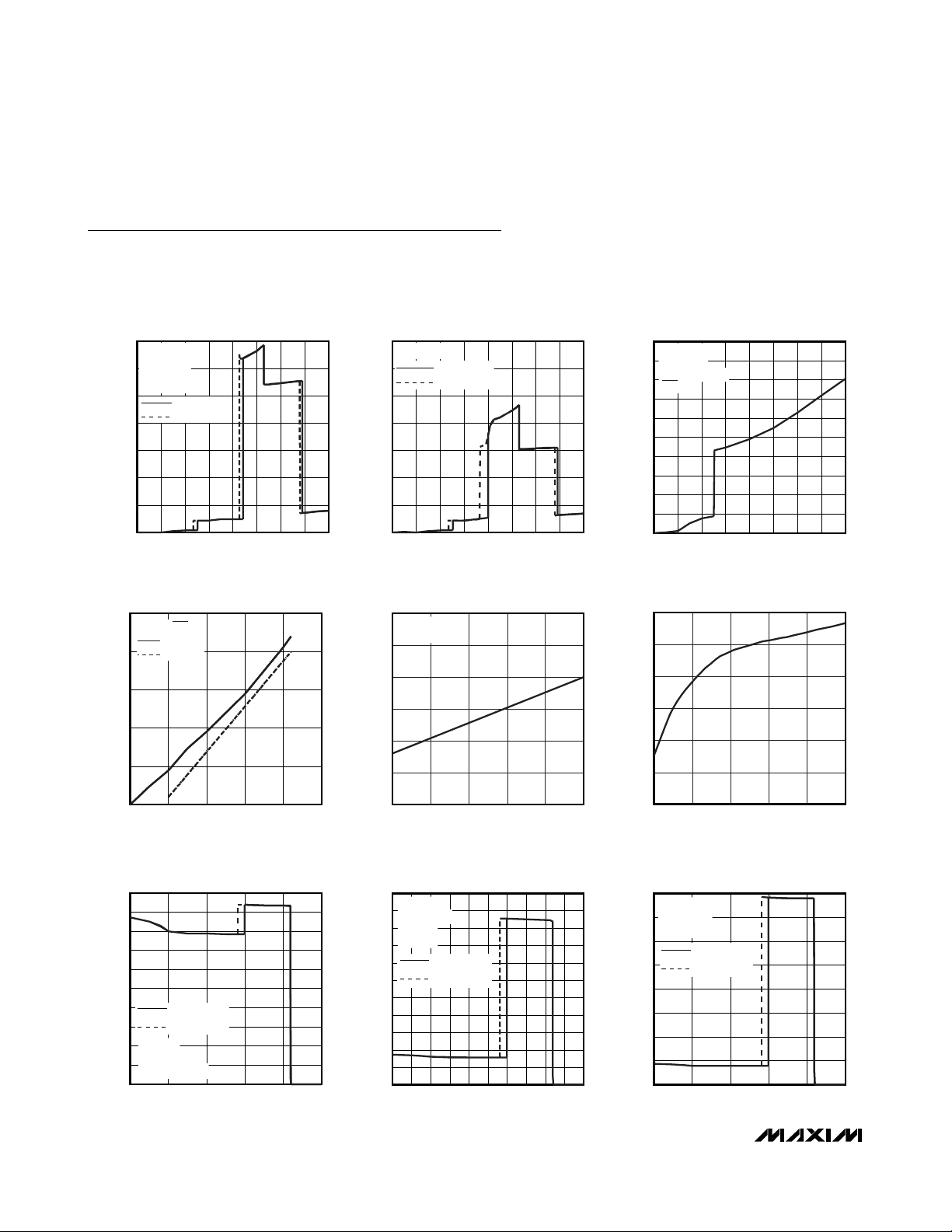
Typical Operating Characteristics
(Circuit of Figure 1, V
DC
= 5V, R
PSET
= 1.5kΩ, R
ISET
= 3kΩ, V
OUT1
= 3.3V, V
OUT2
= 1.3V, SL1 = SL2 = open, V
CEN
= 0V, V
PEN1
=
V
PEN2
= 5V, C
OUT1
= 2 x 10µF, C
OUT2
= 2 x 10µF, C
OUT3
= 0.1µF, C
OUT4
= 4.7µF, C
OUT5
= 1µF, C
OUT6
= 2.2µF, C
OUT7
= 1µF, CT =
0.068µF, C
REF
= CVL= 0.1µF, R
THM
= 10kΩ, L1 = 3.3µH, L2 = 4.7µH, L3 = 22µH, GND = PG1 = PG2 = PG3 = 0, TA= +25°C, unless
otherwise noted.)
INPUT QUIESCENT CURRENT
vs. INPUT VOLTAGE (CHARGER ENABLED)
MAX8662/63 toc01
INPUT VOLTAGE (V)
INPUT QUIESCENT CURRENT (mA)
7654321
0.2
0.4
0.6
0.8
1.0
1.2
1.4
0
08
V
BAT
= 4.2V
I
SYS
= 0
CHARGER IN
DONE MODE
V
BAT
RISING
V
BAT
FALLING
INPUT QUIESCENT CURRENT
vs. INPUT VOLTAGE (CHARGER DISABLED)
MAX8662/63 toc02
INPUT VOLTAGE (V)
INPUT QUIESCENT CURRENT (mA)
7654321
0.2
0.4
0.6
0.8
1.0
1.2
1.4
0
08
V
BAT
= 3.6V
V
BAT
RISING
V
BAT
FALLING
INPUT QUIESCENT CURRENT
vs. INPUT VOLTAGE (SUSPEND)
MAX8662/63 toc03
INPUT VOLTAGE (V)
INPUT QUIESCENT CURRENT (mA)
764 52 31
0.02
0.04
0.06
0.08
0.10
0.12
0.14
0.16
0.18
0.20
0
08
V
BAT
= 4.2V
I
SYS
= 0mA
PEN1 = PEN2 = 0
CEN = 1
BATTERY-LEAKAGE CURRENT
vs. BATTERY VOLTAGE
MAX8662/63 toc04
BATTERY VOLTAGE (V)
BATTERY-LEAKAGE CURRENT (μA)
4321
0.1
0.2
0.3
0.4
0.5
0
05
EN_ = 0, CEN = 1
V
DC
OPEN
V
DC
= 5V
BATTERY-LEAKAGE CURRENT
vs. TEMPERATURE (INPUT DISCONNECTED)
MAX8662/63 toc05
AMBIENT TEMPERATURE (°C)
BATTERY-LEAKAGE CURRENT (μA)
603510-15
0.3
0.5
0.4
0.6
0.7
0.8
0.2
-40 85
V
BAT
= 4.0V
EN_ = 0
BATTERY-REGULATION VOLTAGE
vs. TEMPERATURE
MAX8662/63 toc06
AMBIENT TEMPERATURE (°C)
BATTERY-REGULATION VOLTAGE (V)
603510-15
4.180
4.175
4.185
4.195
4.190
4.200
4.170
-40 85
EN_ = 0
CHARGE CURRENT
vs. BATTERY VOLTAGE (100mA USB)
MAX8662/63 toc07
BATTERY VOLTAGE (V)
CHARGE CURRENT (mA)
4321
10
20
30
40
50
60
70
80
90
100
0
05
VDC = 5V
R
ISET
= 3kΩ
PEN1 = PEN2 = 0
V
BAT
FALLING
V
BAT
RISING
CHARGE CURRENT
vs. BATTERY VOLTAGE (500mA USB)
MAX8662/63 toc08
BATTERY VOLTAGE (V)
CHARGE CURRENT (mA)
4.54.03.0 3.51.0 1.5 2.0 2.50.5
50
100
150
200
250
300
350
400
450
500
550
0
05.0
VDC = 5V
R
ISET
= 3k
Ω
PEN1 = 0
PEN2 = 1
V
BAT
FALLING
V
BAT
RISING
CHARGE CURRENT
vs. BATTERY VOLTAGE (AC ADAPTER)
MAX8662/63 toc09
BATTERY VOLTAGE (V)
CHARGE CURRENT (mA)
431 2
100
200
300
400
600
500
700
800
0
05
VDC = 5V
R
ISET
= 3k
Ω
PEN1 = PEN2 = 1
V
BAT
FALLING
V
BAT
RISING
Page 9
MAX8662/MAX8663
Power-Management ICs for
Single-Cell, Li+ Battery-Operated Devices
_______________________________________________________________________________________
9
CHARGE CURRENT vs. AMBIENT TEMPERATURE
(LOW IC POWER DISSIPATION)
MAX8662/63 toc10
AMBIENT TEMPERATURE (°C)
CHARGE CURRENT (mA)
603510-15
100
200
300
400
500
600
700
800
900
0
-40 85
PEN1 = PEN2 = 1
PEN1 = PEN2 = 0
PEN1 = 0, PEN2 = 1
VDC = 5.0V, V
BAT
= 4.0V
R
ISET
= 3kΩ, CEN = 0, EN_ = 0
CHARGE CURRENT vs. AMBIENT TEMPERATURE
(HIGH IC POWER DISSIPATION)
MAX8662/63 toc11
AMBIENT TEMPERATURE (°C)
CHARGE CURRENT (mA)
603510-15
100
200
300
400
500
600
700
800
900
0
-40 85
PEN1 = PEN2 = 1
PEN1 = PEN2 = 0
PEN1 = 0, PEN2 = 1
VDC = 6.5V, V
BAT
= 3.1V
R
ISET
= 3kΩ, CEN = 0, EN_ = 0
SYS OUTPUT VOLTAGE
vs. INPUT VOLTAGE
MAX8662/63 toc12
INPUT VOLTAGE (V)
V
SYS
(V)
76
53412
3.8
4.2
4.0
4.6
4.4
5.2
5.0
4.8
5.4
5.6
3.6
08
V
BAT
= 4.0V
I
SYS
= 0mA
PEN1 = 0
PEN2 = 1
CHARGER
DISABLED
CHARGER
ENABLED
SYS OUTPUT VOLTAGE
vs. SYS OUTPUT CURRENT (DC DISCONNECTED)
MAX8662/63 toc13
I
SYS
(A)
V
SYS
(V)
2.52.01.51.00.5
3.8
4.0
4.2
4.4
4.6
4.8
5.0
5.2
5.4
5.6
3.6
03.0
V
BAT
= 4.0V
V
DC
= 0V
THE SLOPE OF THIS LINE SHOWS THAT THE
BAT-TO-SYS RESISTANCE IS 49mΩ.
SYS OUTPUT VOLTAGE
vs. SYS OUTPUT CURRENT (500mA USB)
MAX8662/63 toc14
I
SYS
(A)
V
SYS
(V)
2.52.01.51.00.5
3.8
4.0
4.2
4.4
4.6
4.8
5.0
5.2
5.4
5.6
3.6
03.0
VDC = 5.0V
V
BAT
= 4.0V
PEN1 = 0, PEN2 = 1
CEN = 1
SYS OUTPUT VOLTAGE
vs. SYS OUTPUT CURRENT (AC ADAPTER)
MAX8662/63 toc15
I
SYS
(A)
V
SYS
(V)
2.52.01.51.00.5
3.8
4.0
4.2
4.4
4.6
4.8
5.0
5.2
5.4
5.6
3.6
03.0
VDC = 5.0V
V
BAT
= 4.0V
PEN1 = PEN2 = 1
CEN = 1
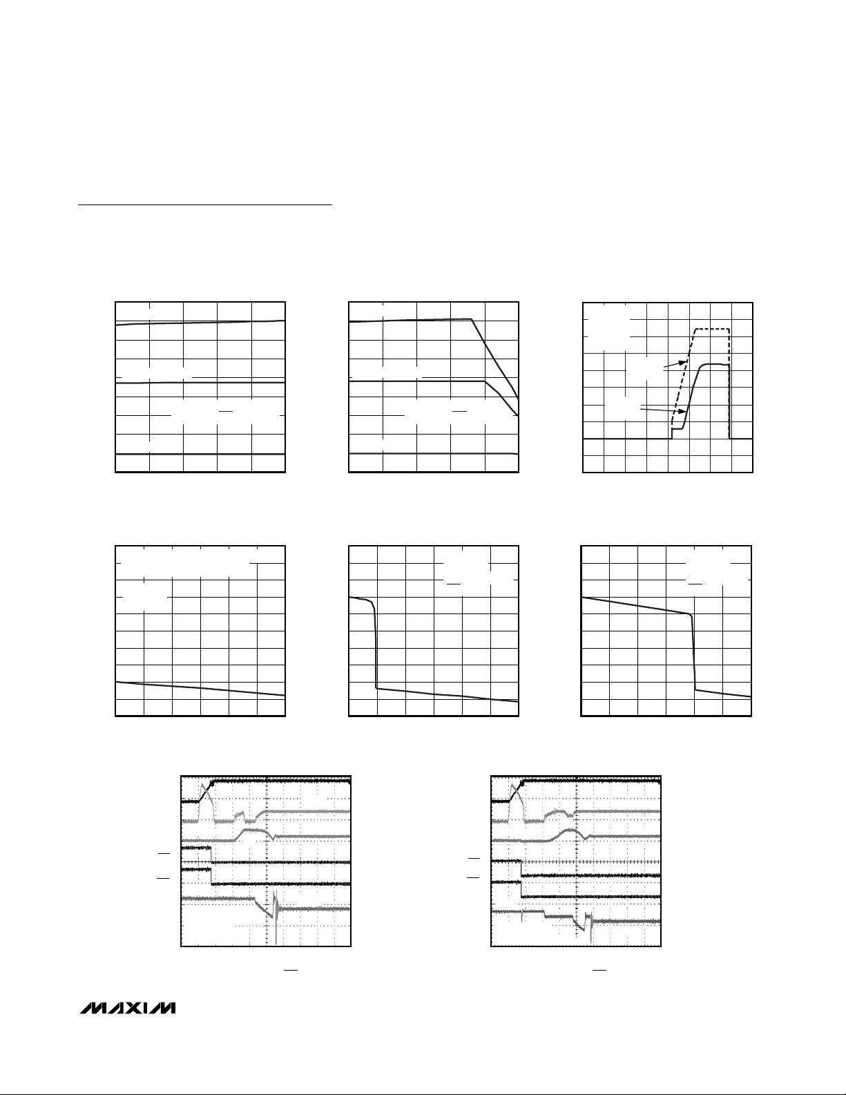
USB CONNECT (I
SYS
= 0mA)
MAX8662/63 toc16
200μs/div
PEN1 = PEN2 = 0, CEN = 0,
V
BAT
= 4.0V, I
SYS
= 0mA, EN_ = 1
V
DC
I
IN
V
SYS
V
POK
V
CHG
I
BAT
0V
0V
0mA
0mA
4.0V
5V
4.4V
5V
+95mA
+95mA
5V/div
5V/div
5V/div
2V/div
200mA/div
200mA/div
NEGATIVE BATTERY
CURRENT FLOWS INTO
THE BATTERY
(CHARGING).
USB CONNECT (I
SYS
= 50mA)
MAX8662/63 toc17
200μs/div
PEN1 = PEN2 = 0, CEN = 0,
V
BAT
= 4.0V, I
SYS
= 50mA, EN_ = 1
V
DC
I
IN
V
SYS
V
POK
V
CHG
I
BAT
NEGATIVE BATTERY
CURRENT FLOWS
INTO THE BATTERY (CHARGING).
0V
0V
0V
0mA
50mA
4.0V
4.4V
5V/div
5V/div
5V/div
2V/div
200mA/div
200mA/div
5V
5V
+95mA
-45mA
Typical Operating Characteristics (continued)
(Circuit of Figure 1, V
DC
= 5V, R
PSET
= 1.5kΩ, R
ISET
= 3kΩ, V
OUT1
= 3.3V, V
OUT2
= 1.3V, SL1 = SL2 = open, V
CEN
= 0V, V
PEN1
=
V
PEN2
= 5V, C
OUT1
= 2 x 10µF, C
OUT2
= 2 x 10µF, C
OUT3
= 0.1µF, C
OUT4
= 4.7µF, C
OUT5
= 1µF, C
OUT6
= 2.2µF, C
OUT7
= 1µF, CT =
0.068µF, C
REF
= CVL= 0.1µF, R
THM
= 10kΩ, L1 = 3.3µH, L2 = 4.7µH, L3 = 22µH, GND = PG1 = PG2 = PG3 = 0, TA= +25°C, unless
otherwise noted.)
Page 10
MAX8662/MAX8663
Power-Management ICs for
Single-Cell, Li+ Battery-Operated Devices
10 ______________________________________________________________________________________
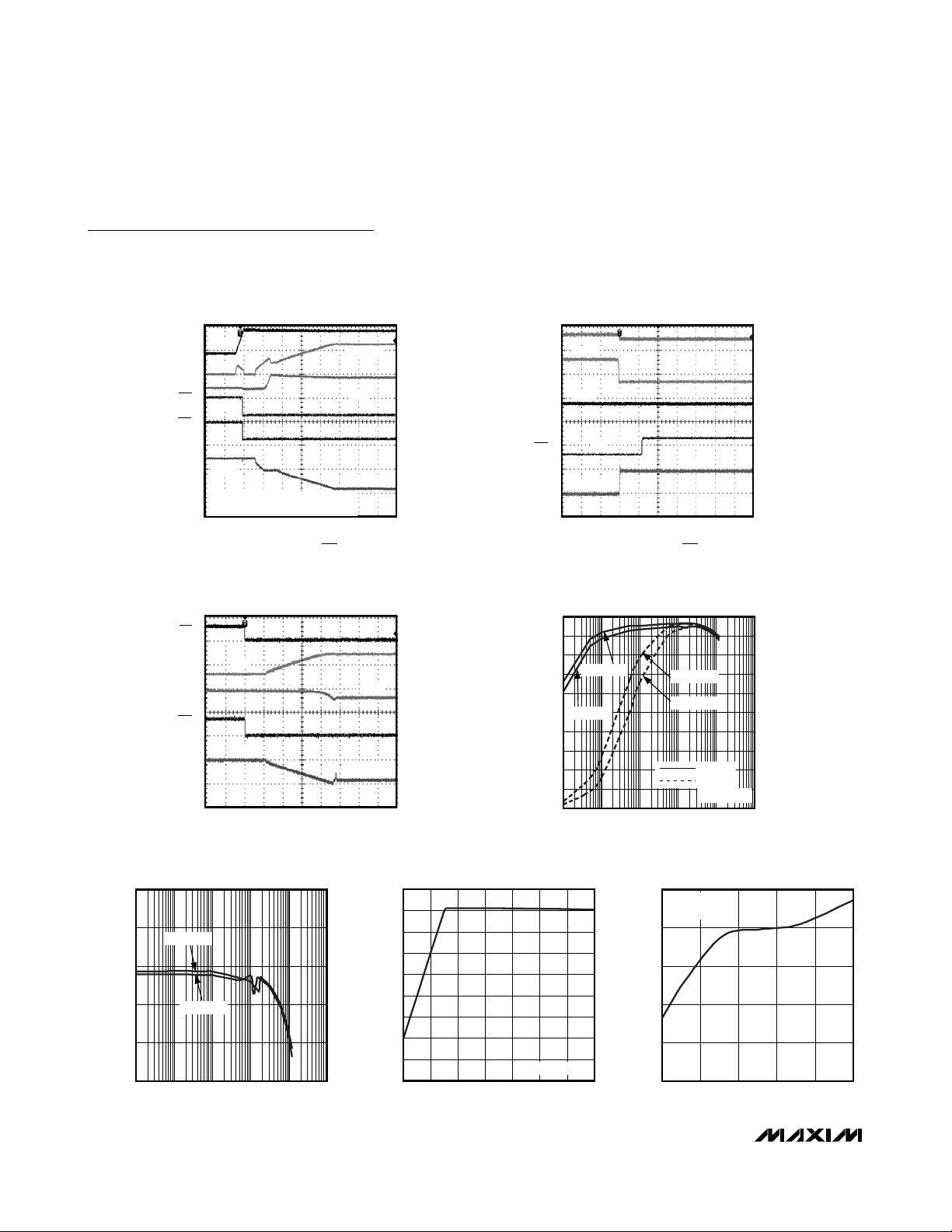
AC ADAPTER CONNECT (I
SYS
= 500mA)
MAX8662/63 toc18
400μs/div
PEN1 = PEN2 = 1, CEN = 0,
V
BAT
= 4.0V, I
SYS
= 500mA, EN_ = 1
V
DC
I
IN
V
SYS
V
POK
V
CHG
I
BAT
NEGATIVE BATTERY CURRENT FLOWS
INTO THE BATTERY (CHARGING).
0V
0V
0mA
500mA
4.0V
4.4V
5V
5V/div
5V/div
5V/div
2V/div
1A/div
1A/div
5V
+1280mA
-780mA
USB DISCONNECTED (500mA USB)
MAX8662/63 toc19
200μs/div
PEN1 = 0, PEN2 = 1, CEN = 0,
V
BAT
= 4.0V, I
SYS
= 0mA
V
DC
I
IN
V
SYS
V
CHG
I
BAT
0V
0mA
4.4V
5V
5V/div
5V/div
500mA/div
500mA/div
1V/div
475mA
-475mA
CHARGER ENABLE (I
SYS
= 0mA)
MAX8662/63 toc20
200μs/div
PEN1 = 0, PEN2 = 1, V
BAT
= 4.0V, I
SYS
= 0mA, EN_ = 1
V
CEN
I
IN
V
SYS
V
CHG
I
BAT
2.8V
0V
0mA
0mA
5V
4.4V
0V
475mA
-475mA
5V/div
5V/div
500mA/div
2V/div
1A/div
OUT1 REGULATOR EFFICIENCY
vs. LOAD CURRENT
MAX8662/63 toc21
LOAD CURRENT (mA)
OUT1 REGULATOR EFFICIENCY (%)
1000100101
10
20
30
40
50
60
70
80
90
100
0
0.1 10,000
V
BAT
= 4.2V
V
BAT
= 3.6V
PWM = 0
PWM = 1
V
BAT
= 4.2V
V
BAT
= 3.6V
V
OUT1
= 3.3V
Typical Operating Characteristics (continued)
(Circuit of Figure 1, V
DC
= 5V, R
PSET
= 1.5kΩ, R
ISET
= 3kΩ, V
OUT1
= 3.3V, V
OUT2
= 1.3V, SL1 = SL2 = open, V
CEN
= 0V, V
PEN1
=
V
PEN2
= 5V, C
OUT1
= 2 x 10µF, C
OUT2
= 2 x 10µF, C
OUT3
= 0.1µF, C
OUT4
= 4.7µF, C
OUT5
= 1µF, C
OUT6
= 2.2µF, C
OUT7
= 1µF, CT =
0.068µF, C
REF
= CVL= 0.1µF, R
THM
= 10kΩ, L1 = 3.3µH, L2 = 4.7µH, L3 = 22µH, GND = PG1 = PG2 = PG3 = 0, TA= +25°C, unless
otherwise noted.)
OUT1 REGULATOR LINE REGULATION
MAX8662/63 toc23
V
SYS
(V)
OUTPUT VOLTAGE (V)
5.14.73.9 4.33.53.1
2.6
2.7
2.8
2.9
3.0
3.1
3.2
3.3
3.4
2.5
2.7 5.5
R
LOAD
= 330Ω
OUT1 VOLTAGE vs. TEMPERATURE
MAX8662/63 toc24
AMBIENT TEMPERATURE (°C)
OUTPUT VOLTAGE (V)
603510-15
3.294
3.298
3.302
3.306
3.310
3.290
-40 85
V
BAT
= 4.0V
R
LOAD
= 330Ω
OUT1 REGULATOR LOAD REGULATION
MAX8662/63 toc22
LOAD CURRENT (mA)
OUTPUT VOLTAGE (V)
1000100101
3.24
3.28
3.32
3.36
3.40
3.20
0.1 10,000
V
BAT
= 4.2V
V
BAT
= 3.6V
Page 11
MAX8662/MAX8663
Power-Management ICs for
Single-Cell, Li+ Battery-Operated Devices
______________________________________________________________________________________
11
OUT1 REGULATOR LIGHT-LOAD
SWITCHING WAVEFORMS
MAX8662/63 toc25
20μs/div
V
OUT1
AC-COUPLED
V
LX
I
L
50mV/div
2V/div
200mA/div
V
BAT
= 4.0V
I
OUT1
= 10mA
PWM = 0
OUT1 REGULATOR HEAVY-LOAD
SWITCHING WAVEFORMS
MAX8662/63 toc26
1μs/div
V
OUT1
AC-COUPLED
V
LX
I
L
10mV/div
2V/div
500mA/div
V
BAT
= 4.2V
I
OUT1
= 1200mA
OUT1 REGULATOR LOAD-
TRANSIENT RESPONSE
MAX8662/63 toc27
40μs/div
V
OUT1
V
LX
I
OUT1
I
L
100mV/div
5V/div
1A/div
1A/div
V
BAT
= 4.0V
I
OUT1
= 10mA TO 1200mA TO 10mA
PWM = 0
OUT1 REGULATOR LINE-
TRANSIENT RESPONSE
MAX8662/63 toc28
100μs/div
V
OUT1
V
SYS
V
LX
I
L
200mA/div
5V/div
50mV/div
1V/div
I
OUT1
= 10mA
PWM = 0
5V
4V
OUT1 ENABLE AND DISABLE RESPONSE
MAX8662/63 toc29
1ms/div
V
OUT1
V
EN1
2V/div
2V/div
I
OUT1
= 10mA
Typical Operating Characteristics (continued)
(Circuit of Figure 1, V
DC
= 5V, R
PSET
= 1.5kΩ, R
ISET
= 3kΩ, V
OUT1
= 3.3V, V
OUT2
= 1.3V, SL1 = SL2 = open, V
CEN
= 0V, V
PEN1
=
V
PEN2
= 5V, C
OUT1
= 2 x 10µF, C
OUT2
= 2 x 10µF, C
OUT3
= 0.1µF, C
OUT4
= 4.7µF, C
OUT5
= 1µF, C
OUT6
= 2.2µF, C
OUT7
= 1µF, CT =
0.068µF, C
REF
= CVL= 0.1µF, R
THM
= 10kΩ, L1 = 3.3µH, L2 = 4.7µH, L3 = 22µH, GND = PG1 = PG2 = PG3 = 0, TA= +25°C, unless
otherwise noted.)
OUT2 REGULATOR EFFICIENCY
vs. LOAD CURRENT
MAX8662/63 toc30
LOAD CURRENT (mA)
OUT2 REGULATOR EFFICIENCY (%)
100101
10
20
30
40
50
60
70
80
90
100
0
0.1 1000
V
BAT
= 4.2V
V
BAT
= 4.2V
V
BAT
= 3.6V
V
BAT
= 3.6V
PWM = 0
PWM = 1
V
OUT1
= 3.3V
MAX8662/63 toc31
LOAD CURRENT (mA)
OUTPUT VOLTAGE (V)
1000100101
1.27
1.28
1.29
1.30
1.31
1.32
1.26
0.1 10,000
OUT2 REGULATOR LOAD REGULATION
V
BAT
= 3.6V
V
BAT
= 4.2V
Page 12

MAX8662/MAX8663
Power-Management ICs for
Single-Cell, Li+ Battery-Operated Devices
12 ______________________________________________________________________________________
OUT2 REGULATOR LINE-
TRANSIENT RESPONSE
MAX8662/63 toc37
100μs/div
V
OUT1
I
L
V
SYS
V
LX
200mA/div
1V/div
5V/div
20mV/div
I
OUT1
= 10mA
PWM = 0
4V
5V
OUT2 REGULATOR LINE REGULATION
MAX8662/63 toc32
V
SYS
(V)
OUTPUT VOLTAGE (V)
5.14.3 4.73.93.1 3.5
1.304
1.302
1.306
1.308
1.310
1.300
2.7 5.5
R
LOAD
= 130Ω
OUT2 VOLTAGE vs. TEMPERATURE
MAX8662/63 toc33
AMBIENT TEMPERATURE (°C)
OUTPUT VOLTAGE (V)
603510-15
1.3035
1.3040
1.3045
1.3050
1.3030
-40 85
V
BAT
= 4.0V
R
LOAD
= 130Ω
OUT2 REGULATOR LIGHT-LOAD
SWITCHING WAVEFORMS
MAX8662/63 toc34
10μs/div
V
OUT2
AC-COUPLED
I
L
V
LX
20mV/div
100mA/div
2V/div
V
BAT
= 4.0V
I
OUT2
= 10mA
PWM = 0
OUT2 REGULATOR HEAVY-LOAD
SWITCHING WAVEFORMS
MAX8662/63 toc35
1μs/div
V
OUT2
AC-COUPLED
I
L
V
L
10mV/div
500mA/div
2V/div
V
BAT
= 4.0V
I
OUT2
= 900mA
OUT2 REGULATOR LOAD-
TRANSIENT RESPONSE
MAX8662/63 toc36
40μs/div
I
OUT2
V
OUT2
AC-COUPLED
I
L
V
LX
50mV/div
500mA/div
5V/div
1A/div
V
BAT
= 4.0V
I
OUT2
= 10mA TO 900mA TO 10mA
PWM = 0
Typical Operating Characteristics (continued)
(Circuit of Figure 1, V
DC
= 5V, R
PSET
= 1.5kΩ, R
ISET
= 3kΩ, V
OUT1
= 3.3V, V
OUT2
= 1.3V, SL1 = SL2 = open, V
CEN
= 0V, V
PEN1
=
V
PEN2
= 5V, C
OUT1
= 2 x 10µF, C
OUT2
= 2 x 10µF, C
OUT3
= 0.1µF, C
OUT4
= 4.7µF, C
OUT5
= 1µF, C
OUT6
= 2.2µF, C
OUT7
= 1µF, CT =
0.068µF, C
REF
= CVL= 0.1µF, R
THM
= 10kΩ, L1 = 3.3µH, L2 = 4.7µH, L3 = 22µH, GND = PG1 = PG2 = PG3 = 0, TA= +25°C, unless
otherwise noted.)
Page 13

MAX8662/MAX8663
Power-Management ICs for
Single-Cell, Li+ Battery-Operated Devices
_____________________________________________________________________________________
13
OUT2 ENABLE AND DISABLE RESPONSE
MAX8662/63 toc38
1μs/div
V
OUT2
V
EN2
2V/div
1V/div
I
OUT2
= 10mA
0V
0V
LED CURRENT
vs. PWM DIMMING DUTY CYCLE
MAX8662/63 toc39
DUTY CYCLE (%)
LED CURRENT (mA)
80604020
1.0
0.5
2.0
1.5
2.5
3.5
3.0
4.5
4.0
5.0
0
09070503010 100
V
BAT
= 3.6V
V
BRT
= 0.25V
f = 1kHz
LED CURRENT vs. BRT VOLTAGE
MAX8662/63 toc40
BRT VOLTAGE (V)
LED CURRENT (mA)
1.20.90.60.3
5
10
15
20
25
30
0
01.5
V
BAT
= 3.6V
OUT4 REGULATOR LOAD REGULATION
MAX8662/63 toc44
LOAD CURRENT (mA)
OUTPUT VOLTAGE (V)
400300200100
3.285
3.290
3.295
3.300
3.305
3.310
3.315
3.280
0 500
VIN = 5.5V
VIN = 3.6V
OUT4 REGULATOR LINE REGULATION
MAX8662/63 toc45
V
IN_OUT4
(V)
OUTPUT VOLTAGE (V)
5432
1.8
2.2
3.0
2.6
3.4
1.4
16
R
LOAD
= 330Ω
Typical Operating Characteristics (continued)
(Circuit of Figure 1, V
DC
= 5V, R
PSET
= 1.5kΩ, R
ISET
= 3kΩ, V
OUT1
= 3.3V, V
OUT2
= 1.3V, SL1 = SL2 = open, V
CEN
= 0V, V
PEN1
=
V
PEN2
= 5V, C
OUT1
= 2 x 10µF, C
OUT2
= 2 x 10µF, C
OUT3
= 0.1µF, C
OUT4
= 4.7µF, C
OUT5
= 1µF, C
OUT6
= 2.2µF, C
OUT7
= 1µF, CT =
0.068µF, C
REF
= CVL= 0.1µF, R
THM
= 10kΩ, L1 = 3.3µH, L2 = 4.7µH, L3 = 22µH, GND = PG1 = PG2 = PG3 = 0, TA= +25°C, unless
otherwise noted.)
OUT4 VOLTAGE vs. TEMPERATURE
MAX8662/63 toc46
AMBIENT TEMPERATURE (°C)
OUTPUT VOLTAGE (V)
603510-15
3.309
3.311
3.313
3.315
3.305
3.307
-40 85
V
BAT
= 4.0V
R
LOAD
= 330Ω
OUT3 SWITCHING WAVEFORMS
MAX8662/63 toc41
1μs/div
V
OUT3
AC-COUPLED
I
L
V
LX
100mA/div
200mV/div
10V/div
I
OUT3
= 1mA
OUT3 ENABLE AND DISABLE RESPONSE
MAX8662/63 toc42
40ms/div
V
OUT3
V
EN3
2V/div
10V/div
0V
0V
OUT3 REGULATOR EFFICIENCY
vs. LOAD CURRENT
MAX8662/63 toc43
LOAD CURRENT (mA)
OUT2 REGULATOR EFFICIENCY (%)
20
10
40
30
50
70
60
90
80
100
0
0.1 101100
V
SYS
= 4.2V
V
SYS
= 3.6V
V
SYS
= 5.5V
Page 14

MAX8662/MAX8663
Power-Management ICs for
Single-Cell, Li+ Battery-Operated Devices
14 ______________________________________________________________________________________
Typical Operating Characteristics (continued)
(Circuit of Figure 1, V
DC
= 5V, R
PSET
= 1.5kΩ, R
ISET
= 3kΩ, V
OUT1
= 3.3V, V
OUT2
= 1.3V, SL1 = SL2 = open, V
CEN
= 0V, V
PEN1
=
V
PEN2
= 5V, C
OUT1
= 2 x 10µF, C
OUT2
= 2 x 10µF, C
OUT3
= 0.1µF, C
OUT4
= 4.7µF, C
OUT5
= 1µF, C
OUT6
= 2.2µF, C
OUT7
= 1µF, CT =
0.068µF, C
REF
= CVL= 0.1µF, R
THM
= 10kΩ, L1 = 3.3µH, L2 = 4.7µH, L3 = 22µH, GND = PG1 = PG2 = PG3 = 0, TA= +25°C, unless
otherwise noted.)
OUT4 REGULATOR LOAD-
TRANSIENT RESPONSE
MAX8662/63 toc47
40μs/div
V
OUT4
AC-COUPLED
I
OUT4
500mA/div
50mV/div
V
BAT
= 4.0V
I
OUT4
= 10mA TO 500mA TO 10mA
OUT4 REGULATOR LINETRANSIENT RESPONSE
MAX8662/63 toc48
100μs/div
V
OUT4
AC-COUPLED
V
IN45
2V/div
20mV/div
I
OUT4
= 10mA
3.6V
5V
OUT4 ENABLE AND DISABLE RESPONSE
MAX8662/63 toc49
200μs/div
V
OUT4
V
EN4
2V/div
2V/div
0V
0V
OUT4 REGULATOR DROPOUT VOLTAGE
vs. LOAD CURRENT
MAX8662/63 toc50
LOAD CURRENT (mA)
DROPOUT VOLTAGE (mV)
400300200100
10
40
50
30
20
60
70
90
80
100
0
0 500
THE SLOPE OF THIS LINE SHOWS THAT
THE DROPOUT RESISTANCE OF AN
AVERAGE PART AND BOARD
COMBINATION IS 181mΩ.
OUT5 REGULATOR LOAD REGULATION
MAX8662/63 toc51
LOAD CURRENT (mA)
OUTPUT VOLTAGE (V)
120906030
3.302
3.304
3.308
3.306
3.310
3.300
0150
VIN = 3.6V
VIN = 5.5V
OUT5 REGULATOR LINE REGULATION
MAX8662/63 toc52
V
IN_OUT5
(V)
OUTPUT VOLTAGE (V)
5432
1.8
2.2
3.0
2.6
3.4
1.4
16
R
LOAD
= 330Ω
OUT5 VOLTAGE vs. TEMPERATURE
MAX8662/63 toc53
AMBIENT TEMPERATURE (°C)
OUTPUT VOLTAGE (V)
603510-15
3.305
3.307
3.306
3.309
3.308
3.310
3.304
-40 85
V
BAT
= 4.0V
R
LOAD
= 330Ω
Page 15

MAX8662/MAX8663
Power-Management ICs for
Single-Cell, Li+ Battery-Operated Devices
______________________________________________________________________________________
15
OUT5 REGULATOR LOAD-
TRANSIENT RESPONSE
MAX8662/63 toc54
40μs/div
V
OUT5
AC-COUPLED
I
OUT5
100mA/div
50mV/div
V
BAT
= 4.0V
I
OUT5
= 10mA TO 150mA TO 10mA
OUT5 REGULATOR LINE-
TRANSIENT RESPONSE
MAX8662/63 toc55
100μs/div
V
OUT5
AC-COUPLED
V
IN45
2V/div
20mV/div
I
OUT5
= 10mA
3.6V
5V
OUT5 ENABLE AND DISABLE RESPONSE
MAX8662/63 toc56
200μs/div
V
OUT5
V
EN5
2V/div
2V/div
0V
0V
OUT5 REGULATOR DROPOUT VOLTAGE
vs. LOAD CURRENT
MAX8662/63 toc57
I
OUT
(mA)
DROPOUT VOLTAGE (V)
120906030
10
30
20
40
50
60
70
0
0 150
THE SLOPE OF THIS LINE SHOWS THAT
THE DROPOUT RESISTANCE OF AN
AVERAGE PART AND BOARD
COMBINATION IS 384mΩ.
OUT6 REGULATOR LOAD REGULATION
MAX8662/63 toc58
LOAD CURRENT (mA)
OUTPUT VOLTAGE (V)
250150 20010050
3.294
3.298
3.302
3.306
3.310
3.290
0 300
VIN = 5.5V
VIN = 3.6V
OUT6 REGULATOR LINE REGULATION
MAX8662/63 toc59
V
IN_OUT6
(V)
OUTPUT VOLTAGE (V)
5432
1.8
1.6
2.0
2.4
2.2
3.2
3.0
2.8
2.6
3.4
1.4
16
R
LOAD
= 330Ω
OUT6 VOLTAGE vs. TEMPERATURE
MAX8662/63 toc60
AMBIENT TEMPERATURE (°C)
OUTPUT VOLTAGE (V)
603510-15
3.303
3.305
3.307
3.309
3.301
-40 85
V
BAT
= 4.0V
R
LOAD
= 330Ω
Typical Operating Characteristics (continued)
(Circuit of Figure 1, V
DC
= 5V, R
PSET
= 1.5kΩ, R
ISET
= 3kΩ, V
OUT1
= 3.3V, V
OUT2
= 1.3V, SL1 = SL2 = open, V
CEN
= 0V, V
PEN1
=
V
PEN2
= 5V, C
OUT1
= 2 x 10µF, C
OUT2
= 2 x 10µF, C
OUT3
= 0.1µF, C
OUT4
= 4.7µF, C
OUT5
= 1µF, C
OUT6
= 2.2µF, C
OUT7
= 1µF, CT =
0.068µF, C
REF
= CVL= 0.1µF, R
THM
= 10kΩ, L1 = 3.3µH, L2 = 4.7µH, L3 = 22µH, GND = PG1 = PG2 = PG3 = 0, TA= +25°C, unless
otherwise noted.)
Page 16

MAX8662/MAX8663
Power-Management ICs for
Single-Cell, Li+ Battery-Operated Devices
16 ______________________________________________________________________________________
Typical Operating Characteristics (continued)
(Circuit of Figure 1, V
DC
= 5V, R
PSET
= 1.5kΩ, R
ISET
= 3kΩ, V
OUT1
= 3.3V, V
OUT2
= 1.3V, SL1 = SL2 = open, V
CEN
= 0V, V
PEN1
=
V
PEN2
= 5V, C
OUT1
= 2 x 10µF, C
OUT2
= 2 x 10µF, C
OUT3
= 0.1µF, C
OUT4
= 4.7µF, C
OUT5
= 1µF, C
OUT6
= 2.2µF, C
OUT7
= 1µF, CT =
0.068µF, C
REF
= CVL= 0.1µF, R
THM
= 10kΩ, L1 = 3.3µH, L2 = 4.7µH, L3 = 22µH, GND = PG1 = PG2 = PG3 = 0, TA= +25°C, unless
otherwise noted.)
OUT6 REGULATOR LOAD-
TRANSIENT RESPONSE
MAX8662/63 toc61
40μs/div
V
OUT6
AC-COUPLED
I
OUT6
200mA/div
50mV/div
V
BAT
= 4.0V
I
OUT6
= 10mA TO 300mA TO 10mA
OUT6 REGULATOR LINE-
TRANSIENT RESPONSE
MAX8662/63 toc62
100μs/div
V
OUT6
AC-COUPLED
V
IN67
2V/div
20mV/div
I
OUT6
= 10mA
3.6V
5V
OUT6 ENABLE AND DISABLE RESPONSE
MAX8662/63 toc63
200μs/div
V
OUT6
V
EN6
2V/div
2V/div
0V
0V
OUT6 REGULATOR DROPOUT VOLTAGE
vs. LOAD CURRENT
MAX8662/63 toc64
I
OUT
(mA)
DROPOUT VOLTAGE (mV)
25020015010050
10
30
40
20
50
60
70
80
0
0300
THE SLOPE OF THIS LINE SHOWS THAT
THE DROPOUT RESISTANCE OF AN
AVERAGE PART AND BOARD
COMBINATION IS 238mΩ.
OUT7 REGULATOR LOAD REGULATION
MAX8662/63 toc65
LOAD CURRENT (mA)
OUTPUT VOLTAGE (V)
120906030
3.296
3.300
3.298
3.302
3.304
3.294
0 150
VIN = 5.5V
VIN = 3.6V
OUT7 REGULATOR LINE REGULATION
MAX8662/63 toc66
V
IN_OUT7
(V)
OUTPUT VOLTAGE (V)
5432
1.8
1.6
2.0
2.4
2.2
3.2
3.0
2.8
2.6
3.4
1.4
16
R
LOAD
= 330Ω
OUT7 VOLTAGE vs. TEMPERATURE
MAX8662/63 toc67
AMBIENT TEMPERATURE (°C)
OUTPUT VOLTAGE (V)
603510-15
3.299
3.301
3.300
3.302
3.303
3.298
-40 85
V
BAT
= 4.0V
R
LOAD
= 330Ω
Page 17

MAX8662/MAX8663
Power-Management ICs for
Single-Cell, Li+ Battery-Operated Devices
______________________________________________________________________________________
17
OUT7 REGULATOR LOAD-
TRANSIENT RESPONSE
MAX8662/63 toc68
40μs/div
V
OUT7
AC-COUPLED
I
OUT7
100mA/div
50mV/div
V
BAT
= 4.0V
I
OUT7
= 10mA TO 150mA TO 10mA
OUT7 REGULATOR LINE-
TRANSIENT RESPONSE
MAX8662/63 toc69
100μs/div
V
OUT7
AC-COUPLED
V
IN67
2V/div
20mV/div
I
OUT7
= 10mA
3.6V
5V
OUT7 ENABLE AND DISABLE RESPONSE
MAX8662/63 toc70
200μs/div
V
OUT7
V
EN7
2V/div
2V/div
0V
0V
OUT7 REGULATOR DROPOUT VOLTAGE
vs. LOAD CURRENT
MAX8662/63 toc71
I
OUT
(mA)
DROPOUT VOLTAGE (V)
125100755025
10
30
20
40
50
60
70
0
0 150
THE SLOPE OF THIS LINE SHOWS THAT
THE DROPOUT RESISTANCE OF AN
AVERAGE PART AND BOARD
COMBINATION IS 391mΩ.
MAX8662/63 toc72
LOAD CURRENT (mA)
OUTPUT VOLTAGE (V)
86429753
3.25
3.27
3.28
3.26
3.29
3.30
3.31
3.24
01 10
VL REGULATOR LOAD REGULATION
VIN = 5.5V
VIN = 4.35V
MAX8662/63 toc73
VIN (V)
OUTPUT VOLTAGE (V)
7654
3.10
3.05
3.20
3.30
3.15
3.25
3.35
3.40
3.45
3.50
3.00
38
VL REGULATOR LINE REGULATION
R
LOAD
= 3.3kΩ
MAX8662/63 toc74
I
SINK
(mA)
OUTPUT LOW VOLTAGE (V)
3530252015105
0.1
0.2
0.3
0.4
0.5
0
040
VIN = 5.0V
V
BAT
= 4.0V
THE SLOPE OF THIS LINE SHOWS THAT
THE PULLDOWN RESISTANCE IS 11Ω.
PULLDOWN DEVICE HAS A
20mA STEADY-STATE RATING
OPEN-DRAIN OUTPUT VOLTAGE LOW
vs. SINK CURRENT
Typical Operating Characteristics (continued)
(Circuit of Figure 1, V
DC
= 5V, R
PSET
= 1.5kΩ, R
ISET
= 3kΩ, V
OUT1
= 3.3V, V
OUT2
= 1.3V, SL1 = SL2 = open, V
CEN
= 0V, V
PEN1
=
V
PEN2
= 5V, C
OUT1
= 2 x 10µF, C
OUT2
= 2 x 10µF, C
OUT3
= 0.1µF, C
OUT4
= 4.7µF, C
OUT5
= 1µF, C
OUT6
= 2.2µF, C
OUT7
= 1µF, CT =
0.068µF, C
REF
= CVL= 0.1µF, R
THM
= 10kΩ, L1 = 3.3µH, L2 = 4.7µH, L3 = 22µH, GND = PG1 = PG2 = PG3 = 0, TA= +25°C, unless
otherwise noted.)
Page 18

MAX8662/MAX8663
Power-Management ICs for
Single-Cell, Li+ Battery-Operated Devices
18 ______________________________________________________________________________________
Pin Description
PIN
FUNCTION
1 1 PEN1
Inp ut Li m i ter - C ontr ol Inp ut 1. U sed w i th CE N and P E N 2 to set the D C cur r ent l i m i t to 95m A,
475m A, a r esi st or p r og r am m ab l e l evel up to 2A, or to tur n off the i np ut l i m i ter ( see Tab l e 1) .
2 2 PEN2
Inp ut Li m i ter - C ontr ol Inp ut 2. U sed w i th CE N and P E N 1 to set the D C cur r ent l i m i t to 95m A,
475m A, a r esi st or p r og r am m ab l e l evel up to 2A, or to tur n off the i np ut l i m i ter ( see Tab l e 1) .
3 — EN3
Enable Input and PWM Dimming Input for Regulator 3 White LED Boost. Drive high to
enable. Drive low for more than 2ms to turn off. For PWM-controlled dimming, drive EN3
with a PWM switching input with a frequency of 1kHz to 100kHz.
4, 5 3, 4
DC1,
DC2
DC Input Source. Connect to an AC adapter or USB source. DC1 and DC2 are internally
connected.
6, 7 5, 6
SYS1,
SYS2
System Supply Voltage. The SYS output supplies power to all regulators. With no external
power, SYS1 and SYS2 connect to BAT through an internal 40mΩ switch. When a valid
voltage is present at DC_, SYS_ connects to DC_ but is limited to 5.3V. SYS1 and SYS2 are
internally connected.
8, 9 7, 8
BAT1,
BAT2
Battery Connections. Connect to a single-cell Li+ battery. The battery is charged from SYS_
when a valid source is present at DC. BAT_ drives SYS_ when DC is not valid. BAT1 and
BAT2 are internally connected.
10 — BRT
LED Analog Brightness Control Input. Connect BRT to a voltage from 50mV to 1.5V to set
I
CS
from 1mA to 30mA. Connect BRT to the center of a resistor-divider connected between
REF and GND to set a fixed brightness when analog dimming is not required.
11 9 CHG
Charger Status Output. CHG is an open-drain nMOS that pulls low when the charger is in
fast charge or prequalification modes. CHG goes high impedance when the charger is in
top-off mode or disabled.
12 10 CEN
Charger Enable Input. Drive CEN low to enable the charger when a valid source is
connected at DC. Drive CEN high to disable charging. Drive CEN high and PEN2 low to
enter USB suspend mode.
13 11 THM
Thermistor Input. Connect a 10kΩ negative temperature coefficient (NTC) thermistor from
THM to GND. Charging is suspended when the temperature is beyond the hot or cold
limits. Connect THM to GND to disable the thermistor functionality.
14 12 ISET
Charge Rate-Set Input. Connect a resistor from ISET to GND to set the fast-charge current
from 300mA to 1.25A. The prequalification charge current and top-off threshold are set to
10% and 7.5% of fast-charge current, respectively.
15 13 CT
Charge Timer-Programming Pin. Connect a capacitor from CT to GND to set the length of
time required to trigger a fault condition in fast-charge or prequalification mode and to
determine the time the charger remains in top-off mode. Connect CT to GND to disable
timers.
16 — REF
Reference Voltage. Provides 1.5V output when EN3 is high. An internal discharge
resistance pulls REF to 0V when EN3 is low.
17 14 GND Ground. Low-noise ground connection.
18 15
Linear Regulator 4 Output. Delivers up to 500mA at an output voltage determined by SL1
and SL2. Connect a 4.7µF ceramic capacitor from OUT4 to GND. Increase the value to
10µF if V
OUT4
< 1.5V.
MAX8662 MAX8663
NAME
OUT4
Page 19

MAX8662/MAX8663
Power-Management ICs for
Single-Cell, Li+ Battery-Operated Devices
______________________________________________________________________________________ 19
Pin Description (continued)
PIN
NAME
FUNCTION
19 16 IN45
Input Supply for Linear Regulators 4 and 5. Connect IN45 to a supply voltage between 1.7V
and V
SYS
. Connect at least a 1µF ceramic capacitor from IN45 to GND.
20 17
Linear Regulator 5 Output. Delivers up to 150mA at an output voltage determined by SL1
and SL2. Connect a 1µF ceramic capacitor from OUT5 to GND. Increase the value to 2.2µF
if V
OUT5
< 1.5V.
21 18 EN4 Enable Input for Linear Regulator 4. Drive high to enable.
22 19 EN5 Enable Input for Linear Regulator 5. Drive high to enable.
23 20 PWM
PWM/Skip-Mode Selector. Drive PWM high to force step-down regulators 1 and 2 to
operate in 1MHz forced-PWM mode. Drive PWM low, or connect to GND to allow regulators
1 and 2 to enter skip mode at light loads.
24 21 FB1
Feedback Input for Buck Regulator 1. Connect FB1 to the center of a resistor-divider
connected between OUT1 and GND to set the output voltage between 0.98V and 3.3V.
25 22 EN1 Enable Input for Buck Regulator 1. Drive high to enable.
26 23 PG1
Power Ground for Buck Regulator 1. GND, PG1, PG2, and PG3 must be connected
together externally.
27 24 LX1
Buck Regulator 1 Inductor Connection Node. Connect an inductor from LX1 to the output of
regulator 1.
28 25 PV1
P ow er Inp ut for Buck Reg ul ator 1. C onnect P V 1 to S Y S and d ecoup l e w i th a 10µF or g r eater l ow E S R cap aci tor to GN D . P V 1, P V 2, and S Y S m ust b e connected tog ether exter nal l y.
29 — OVP
LED Boost Overvoltage Input. Connect a resistor from OVP to the boost output to set the
maximum output voltage and to initiate soft-start when EN3 goes high. An internal 20µA
pulldown current from OVP to GND determines the maximum boost voltage. The internal
current is disconnected when EN3 is low. OVP is diode clamped to SYS_.
30 — CS
LED Current Source. Sinks from 1mA to 30mA depending on the voltage at BRT and the
PWM signal at EN3. Driving EN3 low for more than 2ms turns off the current source. V
CS
is
regulated to 0.32V.
31 — CC3
C om p ensati on Inp ut for LE D Boost Regul ator 3. S ee the Boost C onverter w i th Whi te LE D D r i ver
( OU T3, M AX 8662 Onl y) secti on.
32 26 FB2
Feedback Input for Buck Regulator 2. Connect FB2 to the center of a resistor-divider
connected between OUT2 and GND to set the output voltage between 0.98V and 3.3V.
33 27 PV2
Power Input for Buck Regulator 2. Connect PV2 to SYS and decouple with a 10µF or
greater low-ESR capacitor to GND. PV1, PV2, and SYS must be connected together
externally.
34 28 LX2
Buck Regulator 2 Inductor Connection Node. Connect an inductor from LX2 to the output of
regulator 2.
35 29 PG2
P ower Gr ound for Buck Reg ulator 2. GN D , P G1, P G2, and PG3 must b e connected together
exter nal l y.
36 30 EN2 Enable Input for Buck Regulator 2. Drive high to enable.
37 31 EN6 Enable Input for Linear Regulator 6. Drive high to enable.
38 32 EN7 Enable Input for Linear Regulator 7. Drive high to enable.
39 — LX3 Boost Regulator 3 Inductor Connection Node. Connect an inductor from LX3 to SYS_.
MAX8662 MAX8663
OUT5
Page 20

MAX8662/MAX8663
Power-Management ICs for
Single-Cell, Li+ Battery-Operated Devices
20 ______________________________________________________________________________________
Pin Description (continued)
PIN
NAME
FUNCTION
40 — PG3
Power Ground for Boost Regulator 3. GND, PG1, PG2, and PG3 must be connected
together externally.
41 33 OUT6
Linear Regulator 6 Output. Delivers up to 300mA at an output voltage determined by SL1
and SL2. Connect a 2.2µF ceramic capacitor from OUT6 to GND. Increase the value to
4.7µF if V
OUT6
< 1.5V.
42 34 IN67
Input Supply for Linear Regulators 6 and 7. Connect IN67 to a supply voltage of 1.7V to
V
SYS
. Connect at least a 1µF ceramic capacitor from IN67 to GND.
43 35 OUT7
Linear Regulator 7 Output. Delivers up to 150mA at an output voltage determined by SL1
and SL2. Connect a 1µF ceramic capacitor from OUT7 to GND. Increase the value to 2.2µF
if V
OUT7
< 1.5V.
44 36 VL
Input Limiter and Charger Logic Supply. Provides 3.3V when a valid input voltage is
present at DC. Connect a 0.1µF capacitor from VL to GND. VL is capable of providing up to
10mA to an external load when DC is valid.
45 37 SL1
46 38 SL2
Output-Voltage Select Inputs 1 and 2 for Linear Regulators. Leave disconnected, or
connect to GND or SYS to set to one of three states. SL1 and SL2 set the output voltage of
OUT4, OUT5, OUT6, and OUT7 to one of nine combinations. See Table 3.
47 39 PSET
Input Current-Limit Set Input. Connect a resistor (R
PSET
) from PSET to ground to program
the DC input current limit from 500mA to 2A.
48 40 POK
Power-Ok Output. POK is an open-drain nMOS output that pulls low when a valid input is
detected at DC. This output is not affected by the states of PEN1, PEN2, or CEN.
——EP
Exposed Paddle. Connect the exposed paddle to ground. Connecting the exposed paddle
to ground does not remove the requirement for proper ground connections to GND, PG1,
PG2, and PG3. The exposed paddle is attached with epoxy to the substrate of the die,
making it an excellent path to remove heat from the IC.
MAX8662 MAX8663
Page 21

MAX8662/MAX8663
Power-Management ICs for
Single-Cell, Li+ Battery-Operated Devices
______________________________________________________________________________________ 21
Figure 1. Block Diagram and Application Circuit
INPUT FROM AC
ADAPTER/USB
4.1V TO 8V
VLOGIC
R1
SYS
OUT1
0.98V TO 3.3V AT 1.2A
MAIN
R3
OFF
SKIP
SYS
OUT2
0.98V TO 3.3V AT 0.9A
CORE
R5
OFF
SYS
TRI-STATE MODE
INPUTS; SEE TABLE 2
SYS
DC1
DC2
C1
100mV
BATTERY-TO-SYS
SWITCH (ALLOWS
CURRENT TO SYS)
INPUT LIMITER
AND
THERMAL
PROTECTION
MAX8662
MAX8663
+
-
+
-
BATTERY
CHARGER
STEP-UP
LED
DRIVER
1.5V
INPUT-
VOLTAGE
POK
MONITOR
INPUT-TO-SYS
MAIN
STEP-DOWN
REGULATOR
CORE
STEP-DOWN
REGULATOR
LDO OUTPUT-
VOLTAGE
SETTING
CURRENT-
LIMITING
SWITCH
BAT AND DC TO SUPPLY
GND
VL
C2
C4
L1
C5
R2
ON
PWM
C6
L2
C7
R4
ON
C8
{
C9
3.3V
PV1
LX1
PG1
FB1
EN1
PWM
PV2
LX2
PG2
FB2
EN2
IN45
SL1
SL2
IN67
SYS1
SYS2
BAT1
BAT2
THM
BATTERY THERMISTOR
R7
CHG
PEN2
PEN1
ADAPTER
CEN
CT
PSET
ISET
LX3
D1
PG3
OVP
CC3
CS
ANALOG DIMMING
BRT
(0 TO 1.5V)
EN3
PWM BRIGHTNESS
CONTROL AND ENABLE
REF
C3
OUT4
EN4 ON
OUT5
EN5
OUT6
EN6
OUT7
EN7
DONE
500mA
L3
MAIN
BATTERY
VLOGIC
TIMEOUT
CHARGING
100mA
USB
ON
C13
OUT3 AT 30mA
OFF
OFF
OFF
OFF
SYS
SYS
D2
D3
D4
D5
D6
D7
D8
D9 TO SYS
C16
C17
C18
C19
ONLY AVAILABLE
FOR THE MAX8662
OUT4
500mA
OUT5
150mA
OUT6
300mA
OUT7
150mA
C10
C11
R6
OK
OFF
C12
R8
R9
C14
R10
C15
ON
ON
ON
E P
Page 22

MAX8662/MAX8663
Power-Management ICs for
Single-Cell, Li+ Battery-Operated Devices
22 ______________________________________________________________________________________
Detailed Description
The MAX8662/MAX8663 highly integrated PMICs are
designed for use in smart cellular phones, PDAs,
Internet appliances, and other portable devices. They
integrate two synchronous buck regulators, a boost
regulator driving two to seven white LEDs (MAX8662
only), four low dropout (LDO) linear regulators, and a
linear charger for a single-cell Li+ battery. Figure 1 is
the block diagram and application circuit.
SPS circuitry offers flexible power distribution between
an AC adapter or USB source, battery, and system
load, and makes the best use of available power from
the AC adapter/USB input. The battery is charged with
any available power not used by the system load. If a
system load peak exceeds the current limit, supplemental current is taken from the battery. Thermal limiting prevents overheating by reducing power drawn
from the input source.
Two step-down DC-DC converters achieve excellent
light-load efficiency and have on-chip soft-start circuitry; 1MHz switching frequency allows for small external
components. Four LDO linear regulators feature low
quiescent current and operate from inputs as low as
1.7V. This allows the LDOs to operate from the stepdown output voltage to improve efficiency. The white
LED driver features easy adjustment of LED brightness
and open-LED overvoltage protection. A 1-cell Li+
charger has programmable charge current up to 1.25A
and a charge timer.
Smart Power Selector (SPS)
SPS seamlessly distributes power between the external
input, the battery, and the system load (Figure 2). The
basic functions of SPS are:
• With both the external power supply and battery
connected:
a) When the system load requirements exceed the
capacity of the external power input, the battery
supplies supplemental current to the load.
b) When the system load requirements are less than
the capacity of the external power input, the bat-
tery is charged with residual power from the input.
• When the battery is connected and there is no
external power input, the system is powered from
the battery.
• When an external power input is connected and
there is no battery, the system is powered from the
external power input.
A thermal-limiting circuit reduces battery-charge rate and
external power-source current to prevent overheating.
Input Limiter
All regulated outputs (OUT1–OUT7) derive their power
from the SYS output. With an AC adapter or USB source
connected at DC, the input limiter distributes power
from the external power source to the system load and
battery charger. In addition to the input limiter’s primary
function of passing the DC power source to the system
and charger loads at SYS, it performs several additional
functions to optimize use of available power:
• Input Voltage Limiting: If the voltage at DC rises,
SYS limits to 5.3V, preventing an overvoltage of the
system load. A DC voltage greater than 6.9V is considered invalid and the input limiter disconnects the
DC input entirely. The withstand voltage at DC is
guaranteed to be at least 9V. A DC input is also
invalid if it is less than BAT, or less than the DC
undervoltage threshold of 3.5V (falling). With an
invalid DC input voltage, SYS connects to BAT
through a 30mΩ switch.
• Input Overcurrent Protection: The current at DC is
limited to prevent input overload. This current limit
is automatically adjusted to match the capabilities
of source, whether it is a 100mA or 500mA USB
source, or an AC adapter. When the load exceeds
the input current limit, SYS drops to 100mV below
BAT and supplemental load current is provided by
the battery.
Q1 INPUT-TO-SYS
SWITCH
Q2
BATTERY-TO-SYS
SWITCH
(DISCHARGE PATH)
Q3
(CHARGE
PATH)
DC
SYS
BAT
AC ADAPTER
OR
USB INPUT
SYSTEM
LOAD
BATTERY
THM
GND
R
THM
MAX8662
MAX8663
Figure 2. Smart Power Selector Block Diagram
Page 23

MAX8662/MAX8663
Power-Management ICs for
Single-Cell, Li+ Battery-Operated Devices
______________________________________________________________________________________ 23
• Thermal Limiting: The input limiter includes a ther-
mal-limiting circuit that reduces the current drawn
from DC when the IC junction temperature increases
beyond +100°C in an attempt to prevent further
heating. The current limit is be reduced by 5%/°C for
temperatures above +100°C, dropping to 0mA at
+120°C. Due to the adaptive nature of the charging
circuitry, the charger current reduces to 0mA before
the system load is affected by thermal limiting.
• Adaptive Battery Charging: While the system is
powered from DC, the charger can also draw
power from SYS to charge the battery. If the charger load plus system load exceeds the current capability of the input source, an adaptive charger
control loop reduces charge current to prevent the
SYS voltage from collapsing. Maintaining a higher
SYS voltage improves efficiency and reduces
power dissipation in the input limiter by running the
switching regulators at lower current.
Figure 3 shows the SYS voltage and its relationship to
DC and BAT under three conditions:
a) Charger is off and SYS is driven from DC.
b) Charger is on and adaptive charger control is limiting
charge current.
c) The load at SYS is greater than the available input current.
The adaptive battery-charger circuit reduces charging
current when the SYS voltage drops 550mV below DC.
For example, if DC is at 5V, the charge current reduces
to prevent SYS from dropping below 4.45V. When DC is
greater than 5.55V, the adaptive charging circuitry
reduces charging current when SYS drops 300mV
below the 5.3V SYS regulation point (5.0V). Finally, the
circuit prevents itself from pulling SYS down to within
100mV of BAT.
BAT
DC
SYS
(CHARGER OFF)
SYS
(CHARGER ON)
550mV
SYS
(SYS OVERLOAD)
5.3V
100mV
100mV
5.0V
INPUT: 500mA USB
CHARGER: RISET = 4Ω (750mA)
I(SYS) x 30mΩ
I(SYS) x 150mAΩ
475mA
0mA
BAT CHARGE
CURRENT
(CHARGE ON)
4.0V
3.9V
Figure 3. SYS Voltage and Charge Current vs. DC and BAT Voltage
Page 24

MAX8662/MAX8663
Power-Management ICs for
Single-Cell, Li+ Battery-Operated Devices
24 ______________________________________________________________________________________
DC Input Current-Limit Selection
(PEN1/PEN2)
The input current limit can be set to a variety of values
as shown in Table 1. When the PEN1 input is low, a
USB source is expected at DC and the current limit is
set to either 95mA or 475mA by PEN2.
When PEN1 is high, an AC adapter is expected at DC
and the current limit is set based on a programming resistor at PSET. The DC input current limit is calculated from:
I
DC_LIM
= 2000 x (1.5 / R
PSET
)
An exception is when the battery charger is disabled
(CEN high) with PEN2 low, where the MAX8662/
MAX8663 enter USB suspend mode.
Power-OK Output (
POK
)
POK is an active-low open-drain output indicating DC
status. When the voltage at DC is between the undervoltage and the overvoltage thresholds, and is greater
than the BAT voltage, POK pulls low to indicate that
input power is OK. Otherwise, POK is high impedance.
POK is not affected by the states of PEN1, PEN2, or
CEN. POK remains active in thermal overload.
Battery Charger
The battery charger state diagram is illustrated in
Figure 4.
With a valid AC adapter/USB voltage present, the battery charger initiates a charge cycle when the charger
CEN
EXPECTED INPUT TYPE
CHARGER CURRENT LIMIT**
0 0 0 95mA 100mA USB 1556(1.5V / R
ISET
)
0 0 1 475mA 500mA USB 1556(1.5V / R
ISET
)
0 1 X* 2000(1.5V / R
PSET
) AC adapter 1556(1.5V / R
ISET
)
1 X* 0 Off USB suspend Off
1 0 1 475mA 500mA USB Off
1 1 1 2000(1.5V / R
PSET
) AC adapter Off
Table 1. DC Input Current and Charger Current-Limit Select
*X
= Don’t care.
**
The maximum charge will not exceed the DC Input current.
TOGGLE CEN OR
REMOVE AND
RECONNECT AC
ADAPTER/USB
CHARGER OFF
CHG = HIGH-Z
I
BAT
= 0mA
TEMPERATURE
SUSPEND
I
BAT
= 0mA
CHG = PREVIOUS STATE
ANY STATE
TIMER > t
PREQUAL
ANY CHARGING STATE
CEN = 1 OR REMOVE AND
RECONNECT AC
ADAPTER/USB
THERMISTOR
TEMPERATURE OK
TIMER = RESUMED
THERMISTOR
TOO HOT OR TOO COLD
TIMER = RESUMED
V
BAT
< 2.88V
SET TIMER = 0
V
BAT
< 3V
SET TIMER = 0
I
BAT
> I
CHG-MAX
x 12%
SET TIMER = 0
I
BAT
< I
CHG-MAX
x 7.5%
AND V
BAT
= 4.2V
TIMER = t
TOP-OFF
V
BAT
= < 4.1V
SET TIMER = 0
TIMER > t
FST-CHG
(TIMER SUSPENDED IF I
BAT
< I
CHG-MAX
x
20% WHILE V
BAT
< 4.2V)
PREQUALIFICATION
CHG = 0V
I
BAT
= I
CHG-MAX
/ 10
CEN = 0
SET TIMER = 0
DONE
CHG = HIGH-Z
I
BAT
= 0mA
FAST CHARGE
CHG = 0V
I
BAT
= I
CHG-MAX
TOP - OFF
CHG = HIGH - Z
FAULT
POK = 0V
CHG = BLINK AT 1Hz
I
BAT
= 0mA
Figure 4. Charger State Diagram
PEN1 PEN2 DC INPUT CURRENT LIMIT
Page 25

MAX8662/MAX8663
Power-Management ICs for
Single-Cell, Li+ Battery-Operated Devices
______________________________________________________________________________________ 25
is enabled. It first detects the battery voltage. If the battery voltage is less than the BAT prequalification threshold (3.0V), the charger enters prequalification mode in
which the battery charges at 10% of the maximum fastcharge current. This slow charge ensures that the battery is not damaged by fast-charge current while
deeply discharged. Once the battery voltage rises to
3.0V, the charger transitions to fast-charge mode and
applies the maximum charge current. As charging continues, the battery voltage rises until it reaches the battery regulation voltage (4.2V) where charge current
starts tapering down. When charge current decreases
to 7.5% of fast-charge current, the charger enters topoff mode. Top-off charging continues for 30min, then all
charging stops. If the battery voltage subsequently
drops below the 4.1V recharge threshold, charging
restarts and the timers reset.
Charge Current
ISET adjusts the MAX8662/MAX8663 charging current
to match the capacity of the battery. A resistor from
ISET to ground sets the maximum fast-charge current,
the charge current in prequal, and the charge-current
threshold below which the battery is considered completely charged. Calculate these thresholds as follows:
I
CHG-MAX
= 1556 x 1.5V / R
ISET
I
PRE-QUAL
= 10% x I
CHG-MAX
I
TOP-OFF
= 7.5% x I
CHG-MAX
Determine the I
CHG-MAX
value by considering the characteristics of the battery, and not the capabilities of the
expected AC adapter/USB charging input, the system
load, or thermal limitations of the PCB. The MAX8662/
MAX8663 automatically adjust the charging algorithm
to accommodate these factors.
In addition to setting the charge current, ISET also provides a means to monitor battery-charge current. The
output voltage of the ISET pin tracks the charge current
delivered to the battery, and can be used to monitor the
charge rate, as shown in Figure 5. A 1.5V output indicates the battery is being charged at the maximum set
fast-charge current; 0V indicates no charging. This voltage is also used by the charger control circuitry to set
and monitor the battery current. Avoid adding more
than 10pF capacitance directly to the ISET pin. If filtering of the charge-current monitor is necessary, add a
resistor of 100kΩ or more between ISET and the filter
capacitor to preserve charger stability.
Charge Timer
As shown in Figure 3, the MAX8662/MAX8663 feature a
fault timer for safe charging. If prequalification charging
or fast charging does not complete within the time limits,
which are programmed by the timer capacitor at CT, the
charger stops charging and issues a timeout fault.
Charging can be resumed by either toggling CEN or
cycling the DC input voltage.
The MAX8662/MAX8663 support values of CCTfrom
0.01µF to 1µF:
When the charger exits fast-charge mode, CHG goes
high impedance and top-off mode is entered. Top-off
time is also determined by the capacitance at CT:
In fast-charge mode, the fault timer is suspended when
the charge current is limited, by input or thermal limiting, to less than 20% of I
CHG-MAX.
t
C
F
TOP OFF
CT
−
=×300
0 068
min
.
μ
t
C
F
FST CHG
CT
−
=×300
0 068
min
.
μ
t
C
F
PREQUAL
CT
=×30
0 068
min
.
μ
BATTERY-CHARGING CURRENT (A)
ISET VOLTAGE (V)
MONITORING THE BATTERY CHARGE CURRENT WITH V
ISET
0 1556 x (1.5V/R
ISET
)
1.5
0
DISCHARGING
V
ISET
=
R
ISET
1556
x I
BAT
Figure 5. Monitoring the Battery Charge Current with ISET
Output Voltage
Page 26

MAX8662/MAX8663
Power-Management ICs for
Single-Cell, Li+ Battery-Operated Devices
26 ______________________________________________________________________________________
Connect CT to GND to disable the prequalification and
fast-charge timers, allowing the battery to charge indefinitely in top-off mode, or if other system timers are to
be used to control charging.
Charge-Enable Input (CEN)
Driving CEN high disables the battery charger. Driving
CEN low enables the charger when a valid source is
connected at DC. CEN does not affect the input limit
current, except that driving CEN high and PEN2 low
activates USB suspend mode.
In many systems, there is no need for the system controller (typically a microprocessor) to disable the charger because the SPS circuitry independently manages
charging and adapter/battery power hand-off. In these
situations, CEN can be connected to ground.
Charge Status Output (CHG)
CHG is an open-drain output that indicates charger status. CHG is low when the battery charger is in prequalification or fast-charge mode. It is high impedance
when the charger is done, in top-off, or disabled.
The charger faults if the charging timer expires in prequalification or fast charge. In this state, CHG pulses at
1Hz to indicate that a fault occurred.
Battery Charger Thermistor Input (THM)
Battery or ambient temperature can be monitored with
a negative temperature coefficient (NTC) thermistor.
Charging is allowed when the thermistor temperature is
within the allowable range.
The charger enters a temperature suspend state when
the thermistor resistance falls below 3.97kΩ (too hot) or
rises above 28.7kΩ (too cold). This corresponds to a 0
to +50°C range when using a 10kΩ NTC thermistor with
a beta of 3500. The relation of thermistor resistance to
temperature is defined by the following equation:
where:
R
T =
The resistance in ohms of the thermistor at tem-
perature T in Celsius
R
25 =
The resistance in ohms of the thermistor at +25°C
ß = The material constant of the thermistor, which typically ranges from 3000K to 5000K
T = The temperature of the thermistor in °C
Table 2 shows temperature limits for different thermistor
material constants.
Some designs may prefer other trip temperatures. This
can usually be accommodated by connecting a resistor
in series and/or in parallel with the thermistor and/or
using a thermistor with different ß. For example, a
+45°C hot threshold and 0°C cold threshold can be
realized by using a thermistor with a ß of 4250 and connecting 120kΩ in parallel. Since the thermistor resistance near 0°C is much higher than it is near +50°C, a
large parallel resistance lowers the cold threshold,
while only slightly lowering the hot threshold.
Conversely, a small series resistance raises the cold
threshold, while only slightly raising the hot threshold.
The charger timer pauses when the thermistor resistance goes out of range: charging stops and the timer
counters hold their state. When the temperature comes
back into range, charging resumes and the counters
continue from where they left off. Connecting THM to
GND disables the thermistor function.
RT R e
T
=×
+
−
⎛
⎝
⎜
⎞
⎠
⎟
⎧
⎨
⎩
⎫
⎬
⎭
25
1
2731298
β
THERMISTOR ß (K) 3000 (K) 3250 (K) 3500 (K) 3750 (K) 4250 (K)
Resistance at +25°C (kΩ) 1010101010
Resistance at +50°C (kΩ) 4.59 4.30 4.03 3.78 3316
Resistance at 0°C (kΩ) 25.14 27.15 29.32 31.66 36.91
Nominal Hot Trip Temperature (°C) 55 53 50 49 46
Nominal Cold Trip Temperature (°C) -3 -1 0 2 4.5
Table 2. Fault Temperatures for Different Thermistors
Page 27

MAX8662/MAX8663
Power-Management ICs for
Single-Cell, Li+ Battery-Operated Devices
______________________________________________________________________________________ 27
Figure 6 shows a simplified version of the THM input.
Ensure that the physical size of the thermistor is such
that the circuit of Figure 6 does not cause self-heating.
Step-Down DC-DC Converters
(OUT1 and OUT2)
OUT1 and OUT2 are high-efficiency, 1MHz, current-mode
step-down converters with adjustable output voltage.
The OUT1 regulator outputs 0.98V to VINat up to 1200mA
while OUT2 outputs 0.98V to VINat up to 900mA.
OUT1 and OUT2 have individual enable inputs. When
enabled, the OUT1 and OUT2 gradually ramp the output voltage over a 1.6ms soft-start time. This soft-start
eliminates input inrush current spikes.
OUT1 and OUT2 can operate at a 100% duty cycle,
which allows the regulators to maintain regulation at the
lowest possible battery voltage. The OUT1 dropout voltage is 72mV with a 600mA load and the OUT2 dropout
voltage is 90mV with a 450mA load (does not include
inductor resistance). During 100% duty-cycle operation,
the high-side p-channel MOSFET turns on continuously,
connecting the input to the output through the inductor.
Step-Down Converter Operating Modes
OUT1 and OUT2 can operate in either auto-PWM mode
(PWM low) or forced-PWM mode (PWM high). In autoPWM mode, OUT1 and OUT2 enter skip mode when
the load current drops below a predetermined level. In
skip mode, the regulator skips cycles when they are not
needed, which greatly decreases quiescent current
and improves efficiency at light loads. In forced-PWM
mode, the converters operate with a constant 1MHz
switching frequency regardless of output load. Output
voltage is regulated by modulating the switching duty
cycle. Forced-PWM mode is preferred for low-noise
systems, where switching harmonics can occur only at
multiples of the constant-switching frequency and are
easily filtered; however, regulator operating current is
greater and light-load efficiency is reduced.
Synchronous Rectification
Internal n-channel synchronous rectifiers eliminate the
need for external Schottky diodes and improve efficiency.
The synchronous rectifier turns on during the second
half of each switching cycle. During this time, the voltage across the inductor is reversed, and the inductor
current ramps down. In PWM mode, the synchronous
rectifier turns off at the end of the switching cycle. In
GND
10kΩ
THM
GND
THERMAL
CONNECTION
VL
SWITCH OPEN
WHEN CHARGER
DISABLED
ESD
DIODE
55.71kΩ
97.71kΩ
54.43kΩ
V
THM_C
= 2.4V RISING (TYP)
V
THM_H
= 0.9V FALLING (TYP)
V
THM_D
= 0.1V FALLING (TYP)
HOT
COLD
ENABLE THM
BAD TEMP
DISABLE CHARGER
6.43kΩ
60mV HYST
60mV HYST
60mV HYST
MAX8662
MAX8663
-
+
-
+
-
+
Figure 6. Thermistor Input
Page 28

MAX8662/MAX8663
Power-Management ICs for
Single-Cell, Li+ Battery-Operated Devices
28 ______________________________________________________________________________________
skip mode, the synchronous rectifier turns off when the
inductor current falls below the n-channel zero-crossing
threshold or at the end of the switching cycle, whichever occurs first.
Setting OUT1 and OUT2 Output Voltage
Select an output voltage for OUT1 between 0.98V and
V
IN
by connecting FB1 to the center of a resistive voltage-divider between OUT1 and GND. Choose R3
(Figure 1) for a reasonable bias current in the resistive
divider; choose R3 to be between 100kΩ and 200kΩ.
Then, R2 (Figure 1) is given by:
R2 = R3 ((V
OUT1/VFB
) - 1)
where V
FB
= 0.98V. For OUT2, R4 and R5 are calculat-
ed using:
R4 = R5 ((V
OUT2/VFB
) - 1)
OUT1 and OUT2 Inductors
3.3µH and 4.7µH inductors are recommended for the
OUT1 and OUT2 step-down converters. Ensure that the
inductor saturation current rating exceeds the peak
inductor current, and the rated maximum DC inductor
current exceeds the maximum output current. For lower
load currents, the inductor current rating may be
reduced. For most applications, use an inductor with a
current rating 1.25 times the maximum required output
current. For maximum efficiency, the inductor’s DC
resistance should be as low as possible. See Table 4
for component examples.
Boost Converter with White LED Driver
(OUT3, MAX8662 Only)
The MAX8662 contains a boost converter, OUT3, which
drives up to seven white LEDs in series at up to 30mA.
The boost converter regulates its output voltage to
maintain the bottom of the LED stack at 320mV. A 1MHz
switching rate allows for a small inductor and small
input and output capacitors, while also minimizing input
and output ripple.
Reference Voltage
REF is a 1.5V regulated output that is available to drive
the BRT input when the boost converter is enabled.
This voltage can be used to control LED brightness by
driving BRT through a resistor-divider.
Boost Overvoltage Protection (OVP)
OVP limits the maximum voltage of the boost output for
protection against overvoltage due to open or disconnected LEDs. An external resistor between OUT3 and
OVP, with an internal 20µA pulldown current from OVP
to GND, sets the maximum boost output to:
V
BOOST_MAX
= (R
OVP
x 20µA) + 1.25V
For example, with R
OVP
= 1.2MΩ, the OUT3 maximum
voltage is set at 25.25V. The OVP circuit also provides
soft-start to reduce inrush current by ramping the internal pulldown current from 0 to 20µA over 1.25ms at
startup. The 20µA internal current is disconnected
when EN3 goes low.
OUT3 can also be used as a voltage-output boost by
setting R
OVP
for the desired output voltage. When doing
this, the output filter capacitor must be at least 1µF, and
the compensation network should be a 0.01µF capacitor in series with a 10kΩ resistor from CC3 to ground.
Brightness Control (Voltage or PWM)
LED current is set by the voltage at BRT. The V
BRT
range for adjusting output current from 1mA to 30mA is
50mV to 1.5V. Connecting BRT to a 1.5V reference voltage (such as REF) sets LED current to 30mA.
The EN3 input can also be driven by a logic-level PWM
brightness control signal, such as that supplied by a
microcontroller. The allowed PWM frequency range is
from 1kHz to 100kHz. A 100% duty cycle corresponds
to full current set by the BRT pin. The MAX8662 digitally
decodes the PWM brightness signal and eliminates
PWM ripple found in more common PWM brightness
controls. As a result, no external filtering is needed to
prevent intensity ripple at the PWM rate.
In order to properly distinguish between a DC or PWM
control signal, the MAX8662 delays turn-on from the rising edge of EN3, and turn-off from the falling edge of
EN3, by 2ms. If there are no more transitions in the EN3
signal after 2ms, EN3 assumes the control signal is DC
and sets LED brightness based on the DC level. If two rising edges occur within 2ms, the circuit assumes the control is PWM and sets brightness based on the duty cycle.
OUT3 Inductor
For the white LED driver, OUT3, a 22µH inductor is recommended for most applications. For best efficiency,
the inductor’s DC resistance should also be as low as
possible. See Table 4 for component examples.
OUT3 Compensation Capacitor
A compensation capacitor from CC3 to GND ensures
boost converter control stability. For white LED applications, connect a 0.22µF ceramic capacitor from CC3 to
ground when using 0.1µF at OUT3. For OLED applications, connect a 0.01µF capacitor in series with 10kΩ
from CC3 to ground, and a 1µF OUT3 capacitor to
improve boost output load-transient response.
OUT3 Diode Selection
The MAX8662 boost converter’s high-switching frequency demands a high-speed rectification diode (D1)
Page 29

MAX8662/MAX8663
Power-Management ICs for
Single-Cell, Li+ Battery-Operated Devices
______________________________________________________________________________________ 29
for optimum efficiency. A Schottky diode is recommended due to its fast recovery time and low forwardvoltage drop. Ensure the diode’s peak current rating
exceeds the peak inductor current. In addition, the
diode’s reverse breakdown voltage must exceed
VOUT3. See Table 4 for component examples.
Linear Regulators (OUT4, OUT5, OUT6,
and OUT7)
The MAX8662/MAX8663 contain four low-dropout, lowquiescent current, low-operating voltage linear regulators. The maximum output currents for OUT4, OUT5,
OUT6, and OUT7 are 500mA, 150mA, 300mA, and
150mA, respectively. Each regulator has its own enable
input. When enabled, a linear regulator soft-starts by
ramping the outputs at 10V/ms. This limits inrush current when the regulators are enabled.
The LDO output voltages, OUT4, OUT5, OUT6, and
OUT7 are pin programmable by SL1 and SL2 (Table 3).
SL1 and SL2 are intended to be hardwired and cannot
be driven by active logic. Changes to SL1 and SL2
after power-up are ignored.
VL Linear Regulator
VL is the output of a 3.3V linear regulator that powers
the on-chip input limiter and charger control circuitry.
VL is powered from DC and can provide up to 10mA
when a DC source is present. Bypass VL to GND with a
0.1µF capacitor.
Regulator Enable Inputs (EN_)
The OUT1–OUT7 regulators have individual enable
inputs. Drive EN_ high to initiate soft-start and enable
OUT_. Drive EN_ low to disable OUT_. When disabled,
each regulator (OUT1–OUT7) switches in an active
pulldown resistor to discharge the output.
Soft-Start/Inrush Current
The MAX8662/MAX8663 implement soft-start on many
levels to control inrush current and avoid collapsing
source supply voltages. The input-voltage limit and battery charger have a 1.5ms soft-start time. All regulators
also implement soft-start. White LED driver soft-start is
accomplished by ramping the OVP current from 0 to
20µA in 1.25ms. During soft-start, the PWM controller
forces 0% switching duty cycle to avoid an input current surge at turn-on.
Undervoltage and Overvoltage Lockout
DC UVLO
When the DC voltage is below the DC undervoltage
threshold (V
UVLO_DC
, typically 3.5V falling), the
MAX8662/MAX8663 enter DC undervoltage lockout (DC
UVLO). DC UVLO forces the power management circuits to a known dormant state until the DC voltage is
high enough to allow the device to make accurate decisions. In DC UVLO, Q1 is open (Figure 2), the charger is
disabled, POK is high-Z, and CHG is high-Z. The system load switch, Q2 (Figure 2) is closed in DC UVLO,
allowing the battery to power the SYS node. All regulators are allowed to operate from the battery in DC UVLO.
DC OVLO
When the DC voltage is above the DC overvoltage
threshold (V
OVLO_DC
, typically 6.9V), the MAX8662/
MAX8663 enter DC overvoltage lockout (DC OVLO).
DC OVLO mode protects the MAX8662/MAX8663 and
downstream circuitry from high-voltage stress up to 9V.
In DC OVLO, VL is on, Q1 (Figure 2) is open, the charger is disabled, POK is high-Z, and CHG is high-Z. The
system load switch Q2 (Figure 2) is closed in DC
OVLO, allowing the battery to power SYS. All regulators
are allowed to operate from the battery in DC UVLO.
CONNECT SL_ TO: LINEAR REGULATOR OUTPUT VOLTAGES
SL1 SL2 OUT4 (V) OUT5 (V) OUT6 (V) OUT7 (V)
Open circuit Open circuit 3.3 3.3 3.3 3.3
Ground Open circuit 3.3 2.85 1.85 1.85
SYS Open circuit 2.85 2.85 1.85 1.85
Open circuit Ground 3.3 2.85 2.85 1.85
Ground Ground 2.5 3.3 1.5 1.5
SYS Ground 2.5 3.3 1.5 1.3
Open circuit SYS 1.2 1.8 1.1 1.3
Ground SYS 3.3 2.85 1.5 1.5
SYS SYS 1.8 2.5 3.3 2.85
Table 3. SL1 and SL2, Output Voltage Selection
Page 30

MAX8662/MAX8663
Power-Management ICs for
Single-Cell, Li+ Battery-Operated Devices
30 ______________________________________________________________________________________
SYS UVLO
When the SYS voltage falls below the SYS undervoltage
threshold (V
UVLO_SYS
, typically 2.4V falling), the
MAX8662/MAX8663 enter SYS undervoltage lockout
(SYS UVLO). SYS UVLO forces all regulators off. All
regulators assume the states determined by the corresponding enable input (EN_) when the SYS voltage
rises above V
UVLO_SYS
.
Input-Limiter Thermal Limiting
The MAX8662/MAX8663 reduce input-limiter current by
5%/°C when its die temperature exceeds +100°C. The
system load (SYS) has priority over charger current, so
input current is first reduced by lowering charge current. If the junction temperature still reaches +120°C in
spite of charge-current reduction, no current is drawn
from DC, the battery supplies the entire system load,
and SYS is regulated at 100mV below BAT. Note that
this on-chip thermal-limiting circuitry is not related to,
and operates independently from, the thermistor input.
Regulator Thermal-Overload Shutdown
The MAX8662/MAX8663 disable all charger, SYS, and
regulator outputs (except VL) if the junction temperature rises above +165°C, allowing the device to cool.
When the junction temperature cools by approximately
15°C, resume the state they held prior to thermal overload. Note that this on-chip thermal-protection circuitry
is not related to, and operates independently from, the
thermistor input. Also note that thermal-overload shutdown is a fail-safe mechanism. Proper thermal design
should ensure that the junction temperature of the
MAX8662/MAX8663 never exceeds the absolute maximum rating of +150°C.
Applications Information
Step-Down Converters (OUT1 and OUT2)
Capacitor Selection
The input capacitor in a DC-DC converter reduces current peaks drawn from the battery or other input power
source and reduces switching noise in the controller.
The impedance of the input capacitor at the switching
frequency should be less than the input source’s output
impedance so that high-frequency switching currents
do not pass through the input source. The DC-DC converter output capacitor keeps output ripple small and
ensures control-loop stability. The output capacitor must
also have low impedance at the switching frequency.
Ceramic capacitors with X5R or X7R dielectrics are
highly recommended for both input and output capacitors due to their small size, low ESR, and small temperature coefficients.
See Table 4 for example OUT1/OUT2 input and output
capacitors and manufacturers.
FUNCTION PART
C1 Input filter capacitor
4.7µF ± 10% , 16V X 5R cer am i c cap aci tor
M ur ata G RM 188R61C 105KA93B or Tai yo Y ud en E M K107 BJ105KA
C2, C3 VL filter capacitor
0.1µF ±10%, 10V X5R ceramic capacitor (0402)
Murata GRM 155R61A104KA01 or TDK C1005X5R1A104K
C4, C6
4.7µF ±10%, 6.3V X5R ceramic capacitors (0603)
Mutara GRM188R60J475KE
C5, C7
Step-down output filter
capacitors
2 x 10µF ±10%, 6.3V X5R ceramic capacitors (0805)
Murata GRM219R60J106KE19
C8, C9
Linear regulator input filter
capacitors
1.0µF ± 10% , 16V X 5R cer am i c cap aci tor s ( 0603)
M ur ata G RM 188R61C 105KA93B or Tai yo Y ud en E M K107 BJ105KA
C10 SYS output bypass capacitor 10µF ±10%, 6.3V X5R ceramic capacitor
C11 Battery bypass capacitor 4.7µF ±10%, 6.3V X5R ceramic capacitor
C12 Charger timing capacitor
0.068µF ±10%, 10V X5R ceramic capacitor (0402)
TDK C1005X5R1A683K
C13 Boost input bypass capacitor
1.0µF ± 10% , 16V X 5R cer am i c cap aci tor ( 0603)
M ur ata G RM 188R61C 105KA93B or Tai yo Y ud en E M K107BJ105KA
C14
0.1µF ±10%, 50V X7R ceramic capacitor (0603)
Murata GRM188R71H104KA93 or Taiyo Yuden UMK107BJ104KA
C15
Step-up compensation
capacitor
0.22µF ±10%, 10V X5R ceramic capacitor (0402)
Murata GRM155R61A224KE19
Table 4. External Components List (See Figure 1)
COMPONENT
Buck input bypass capacitors
Step-up output filter capacitor
Page 31

MAX8662/MAX8663
Power-Management ICs for
Single-Cell, Li+ Battery-Operated Devices
______________________________________________________________________________________ 31
Table 4. External Components List (See Figure 1) (continued)
COMPONENT FUNCTION PART
C16
C17, C19
C18
D1 Boost rectifier
D2–D8 Display backlighting
D9 CS clamp
L1 OUT1 step-down inductor
L2 OUT2 step-down inductor
L3 OUT3 step-up inductor
R1, R7 Logic output pullup resistors 100kΩ
R2–R5 Step-down feedback resistors R3 and R5 are 200kΩ ±0.1%; R2 and R4 depend on output voltage (±0.1%)
R6 Negative TC thermistor
R8
R9
R10
Linear regulator output filter
capacitor
Linear regulator output filter
capacitors
Linear regulator output filter
capacitor
Input current-limit
programming resistor
Fast charge-current
programming resistor
Step-up overvoltage feedback
resistor
4.7µF ±10%, 6.3V X5R ceramic capacitor (0603)
Murata GRM188R60J475KE19
1.0µF ±10%, 6.3V X5R ceramic capacitors (0603)
Murata GRM188R60J105KA01
2.2µF ±10%, 6.3V X5R ceramic capacitor (0603)
Murata GRM185R60J225KE26
200mA, 30V Schottky diode (SOD-323)
Central CMDSH2-3
30mA surface-mount white LEDs
Nichia NSCW215T
100mA silicon signal diode
Central CMOD4448
3.3µH inductor
TOKO DE2818C 1072AS-3R3M, 1.6A, 50mΩ
4.7µH inductor
TOKO DE2818C 1072AS-4R7M, 1.3A, 70mΩ
22µH inductor
Murata LQH32CN220K53, 250mA, 0.71Ω DCR (3.2mm x 2.5mm x 1.55mm)
or TDK VLF3012AT-220MR33, 330mA, 0.76Ω DCR (2.8mm x 2.6mm x 1.2mm)
Phillips NTC thermistor
P/N 2322-640-63103
10kΩ ±5% at +25°C
1.5kΩ ±1%, for 2A limit
3kΩ ±1%, for 777mA charging
1.2MΩ ±1%, for 25V max output
Page 32

MAX8662/MAX8663
Power-Management ICs for
Single-Cell, Li+ Battery-Operated Devices
32 ______________________________________________________________________________________
Power Dissipation
The MAX8662/MAX8663 have a thermal-limiting circuitry,
as well as a shutdown feature to protect the IC from
damage when the die temperature rises. To allow the
maximum charging current and load current on each
regulator, and to prevent thermal overload, it is important
to ensure that the heat generated by the
MAX8662/MAX8663 is dissipated into the PCB. The
package’s exposed paddle must be soldered to the
PCB, with multiple vias tightly packed under the exposed
paddle to ensure optimum thermal contact to the ground
plane.
Table 5 shows the thermal characteristics of the
MAX8662/MAX8663 packages. For example, the junction-to-case thermal resistance (θJC) of the MAX8663 is
2.7°C/W. When properly mounted on a multilayer PCB,
the junction-to-ambient thermal resistance (θJA) is typically 28°C/W.
PCB Layout and Routing
High switching frequencies and relatively large peak
currents make the PCB layout a very important aspect of
design. Good design minimizes ground bounce, excessive EMI on the feedback paths, and voltage gradients
in the ground plane, which can result in instability or
regulation errors.
A separate low-noise analog ground plane containing
the reference, linear regulator, signal ground, and GND
must connect to the power-ground plane at only one
point to minimize the effects of power-ground currents.
PGND_, DC power, and battery grounds must connect
directly to the power-ground plane. Connect GND to
the exposed paddle directly under the IC. Use multiple
tightly spaced vias to the ground plane under the
exposed paddle to help cool the IC.
Position input capacitors from DC, SYS, BAT, PV1, and
PV2 to the power-ground plane as close as possible to
the IC. Connect input capacitors and output capacitors
from inputs of linear regulators to low-noise analog
ground as close as possible to the IC. Connect the
inductors, output capacitors, and feedback resistors as
close to the IC as possible and keep the traces short,
direct, and wide.
Refer to the MAX8662/MAX8663 evaluation kit for a
suitable PCB layout example.
MAX8663
THIN QFN
(5mm x 5mm)
TOP VIEW
35
36
34
33
12
11
13
PEN2
DC2
SYS1
SYS2
BAT1
14
PEN1
PV2
PV1
LX1
LX2
PG2
EN2
PG1
EN1
12
IN67
4567
27282930 26 24 23 22
OUT7
VL
EN4
OUT5
IN45
OUT4
DC1
FB2
3
25
37
SL1
GND
38
39
40
SL2
PSET
POK
CT
ISET
THM
OUT6
32
15
EN5
EN7
31
16
17
18
19
20
PWM
BAT2
CHG
CEN
FB1
8910
21
EN6
Pin Configurations (continued)
48-PIN THIN QFN (6mm x 6mm) 40-PIN THIN QFN (5mm x 5mm)
SINGLE-LAYER PCB MULTILAYER PCB SINGLE-LAYER PCB MULTILAYER PCB
CONTINUOUS
POWER
2105.3mW
Derate 26.3mW/°C above
+70°C
2963.0mW
Derate 37.0mW/°C above
+70°C
1777.8mW
Derate 22.2mW/°C above
+70°C
2857.1mW
Derate 35.7mW/°C above
+70°C
θ
JA
38°C/W 27°C/W 45°C/W 28°C/W
θ
JC
1.4°C/W 1.4°C/W 1.7°C/W 1.7°C/W
Table 5. MAX8662/MAX8663 Package Thermal Characteristics
DISSIPATION
Page 33

MAX8662/MAX8663
Power-Management ICs for
Single-Cell, Li+ Battery-Operated Devices
______________________________________________________________________________________ 33
Package Information
(The package drawing(s) in this data sheet may not reflect the most current specifications. For the latest package outline information
go to www.maxim-ic.com/packages
.)
QFN THIN.EPS
Page 34

MAX8662/MAX8663
Power-Management ICs for
Single-Cell, Li+ Battery-Operated Devices
34 ______________________________________________________________________________________
Package Information (continued)
(The package drawing(s) in this data sheet may not reflect the most current specifications. For the latest package outline information
go to www.maxim-ic.com/packages
.)
Page 35

MAX8662/MAX8663
Power-Management ICs for
Single-Cell, Li+ Battery-Operated Devices
______________________________________________________________________________________ 35
Package Information (continued)
(The package drawing(s) in this data sheet may not reflect the most current specifications. For the latest package outline information
go to www.maxim-ic.com/packages
.)
QFN THIN.EPS
Page 36

MAX8662/MAX8663
Power-Management ICs for
Single-Cell, Li+ Battery-Operated Devices
Maxim cannot assume responsibility for use of any circuitry other than circuitry entirely embodied in a Maxim product. No circuit patent licenses are
implied. Maxim reserves the right to change the circuitry and specifications without notice at any time.
36
____________________Maxim Integrated Products, 120 San Gabriel Drive, Sunnyvale, CA 94086 408-737-7600
© 2007 Maxim Integrated Products is a registered trademark of Maxim Integrated Products. Inc.
REDUTA
Package Information (continued)
(The package drawing(s) in this data sheet may not reflect the most current specifications. For the latest package outline information
go to www.maxim-ic.com/packages
.)
 Loading...