General Description
The MAX8655 synchronous-PWM buck regulator operates from a 4.5V to 25V input and generates an output
voltage adjustable from 0.7V to 5.5V at loads up to 25A.
Integrated power MOSFETs provide a small footprint,
ease of layout, and reduced EMI. Removing the board
trace inductances ensures the highest efficiency at
high frequency.
The MAX8655 uses peak current-mode control architecture with an adjustable (200kHz to 1MHz), constantswitching frequency, which is externally synchronizable.
The MAX8655’s adjustable current limit uses the inductor’s DC resistance to improve efficiency or an external
sense resistor for higher accuracy. Foldback type current limit is available to reduce the power dissipation
under severe-overload or short-circuit conditions. A reference input is provided for use with a high-accuracy
external reference or for DDR and tracking applications.
Monotonic startup provides safe starting into a prebiased output, where traditional step-down regulators
discharge the output capacitor during soft-start, creating a negative voltage at the output and possibly damaging the load.
A 180° out-of-phase synchronization output is available
for synchronizing with another MAX8655.
An enable input is provided for on/off control and to
facilitate output sequencing. Output-voltage sensing for
programmable overvoltage protection is provided and
is independent of the feedback network to further
enhance the output overvoltage protection.
Overall, the MAX8655 provides enough flexibility for the
experienced user, as well as simplicity and ease of use
for non-power-supply engineers.
Applications
Point-of-Load Power Supplies
Telecom Power
Networking
Nonisolated DC-DC Power Modules
Servers and Workstations
Notebook Computers
IBA Power Supplies
Features
♦ 25A Output Current
♦ Integrated Power MOSFETs
♦ Operates from 4.5V to 25V Supply
♦ 1% FB Voltage Accuracy Over Temperature
♦ Adjustable Output Voltage Down to 0.7V
♦ Adjustable Switching Frequency and External
Synchronization from 200kHz to 1MHz
♦ Multiphase Operation with Accurate Current
Sharing
♦ 180° Phase-Shifted Synchronization
♦ Adjustable Overcurrent Limit
♦ Adjustable Slope Compensation
♦ Selectable Current-Limit Mode: Latch-Off or
Automatic Recovery
♦ Monotonic Output Voltage Rise at Startup into
Prebias Output
♦ Output Sources and Sinks Current for DDR
Applications
♦ Enable Input
♦ Power-OK (POK) Output
♦ Adjustable Soft-Start
♦ Independently Adjustable Overvoltage Protection
MAX8655
Highly Integrated, 25A, Wide-Input,
Internal MOSFET, Step-Down Regulator
________________________________________________________________ Maxim Integrated Products 1
Ordering Information
19-3982; Rev 0; 10/07
For pricing, delivery, and ordering information, please contact Maxim Direct at 1-888-629-4642,
or visit Maxim’s website at www.maxim-ic.com.
PART
TEMP
RANGE
PIN-
PACKAGE
PKG
CODE
MAX8655ETN+
-40°C to +85°C
56 TQFN - E P *
( 8mm x 8m m )
T5688M-4
Pin Configuration appears at end of data sheet.
MAX8655
REFIN
MODE
PGND
AVL
GND
OFF
ON
PVIN
INPUT 7V
TO 28V
SYNC OUTPUT
ENABLE INPUT
POWER-OK OUTPUT
FSYNC INPUT
OUTPUT
0.7V TO 12V
UP TO 25A
LX
VL
AVL
VLGND
VL
IN
CS+
CS-
SCOMP
ILIM2
SS
COMP
FB
OVP
ILIM1
PVIN
LXB
SYNCO
FSYNC
POK
EN
BST
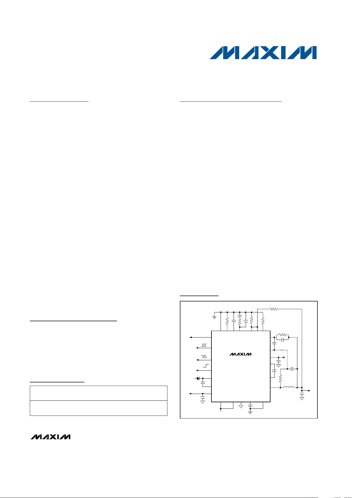
Typical Operating Circuit
+Denotes a lead-free package.
*EP = Exposed pad.
MAX8655
Highly Integrated, 25A, Wide-Input,
Internal MOSFET, Step-Down Regulator
2 _______________________________________________________________________________________
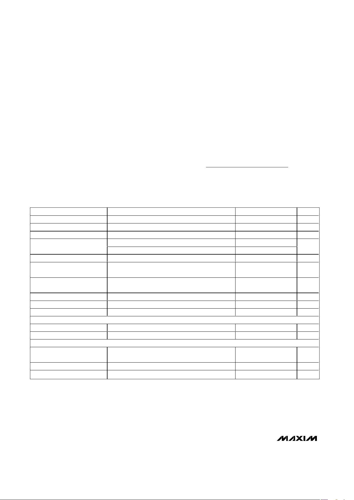
ABSOLUTE MAXIMUM RATINGS
ELECTRICAL CHARACTERISTICS
(VIN= 12V, V
BST
- VLX= 6.5V, TA= -40°C to +85°C, circuit of Figure 4, typical values are at TA= +25°C, unless otherwise noted.) (Note 2)
Stresses beyond those listed under “Absolute Maximum Ratings” may cause permanent damage to the device. These are stress ratings only, and functional
operation of the device at these or any other conditions beyond those indicated in the operational sections of the specifications is not implied. Exposure to
absolute maximum rating conditions for extended periods may affect device reliability.
PVIN, IN, EN to GND ..............................................-0.3V to +30V
BST to LXB ............................................................-0.3V to +7.5V
LX, LXB to GND............ (-2.5V for < 50ns transient) -1V to +30V
ILIM2, ILIM1, SYNCO, FSYNC, OVP,
SCOMP to GND .....................................-0.3V to (V
AVL
+ 0.3V)
VL to PGND ...........................................................-0.3V to +7.5V
AVL, FB, POK, COMP, SS, MODE, REFIN to GND ..-0.3V to +6V
CS+, CS- to GND ....................................................-0.3V to +6V
PGND to GND to VLGND ......................................-0.3V to +0.3V
Operating Junction Temperature Range.......... -40°C to +125°C
Junction Temperature......................................................+150°C
θJC(thermal resistance from
junction to exposed pad) (Note 1) ...............................3.5°C/W
θ
JT
(thermal resistance from junction to the top) ............3.9°C/W
I
LX (RMS)
.................................................................................27A
Storage Temperature Range .............................-65°C to +150°C
Lead Temperature (soldering, 10s) .................................+300°C
PARAMETER CONDITIONS
MIN TYP MAX UNITS
PVIN Operating Voltage Range 3 25 V
IN Operating Voltage Range VL = IN for V
IN
< 7V 4.5
25.0
V
IN Quiescent Supply Current V
FB
= 0.75V, no switching 2 3 mA
EN = GND, V
IN
≤ 28V 10
Shutdown Supply Current
I
IN
+ IVL + I
AVL
, EN = GND, V
AVL
= VVL = VIN = 5V 32
µA
PVIN Shutdown Supply Current V
PVIN
= VLX = V
BST
1 µA
AVL Undervoltage-Lockout
Threshold
V
AVL
rising, 3% typical hysteresis
3.90 4.15 4.40
V
Output-Voltage Adjust Range
Minimum output voltage is limited by minimum duty cycle
and external components
0.7 5.5 V
VL Regulation Voltage 7V < V
IN
< 28V 6.0 6.5 7.0 V
AVL Regulation Voltage 5.5V < V
VL
< 7V, 1mA < I
LOAD
< 10mA
4.900 4.975 5.050
V
AVL Output Current 10 mA
SOFT-START
SS Shutdown Resistance From SS to GND, V
EN
= 0V 20 100 Ω
SS Soft-Start Current V
REF
= 0.625V 18 23 28 µA
REFIN INPUT
REFIN Dual Mode™ Threshold
V
AVL
-
1.0V
V
AVL
V
REFIN Input Bias Current V
REFIN
= 0.7V to 1.5V
-250
+250
nA
REFIN Input Voltage Range 0 1.5 V
Dual Mode is a trademark of Maxim Integrated Products, Inc.
Note 1: Package thermal resistances were obtained using the method described in JEDEC specification JESD51-7, using a 4-layer
board. For detailed information on package thermal considerations, see www.maxim-ic.com/thermal-tutorial
.
MAX8655
Highly Integrated, 25A, Wide-Input,
Internal MOSFET, Step-Down Regulator
_______________________________________________________________________________________ 3
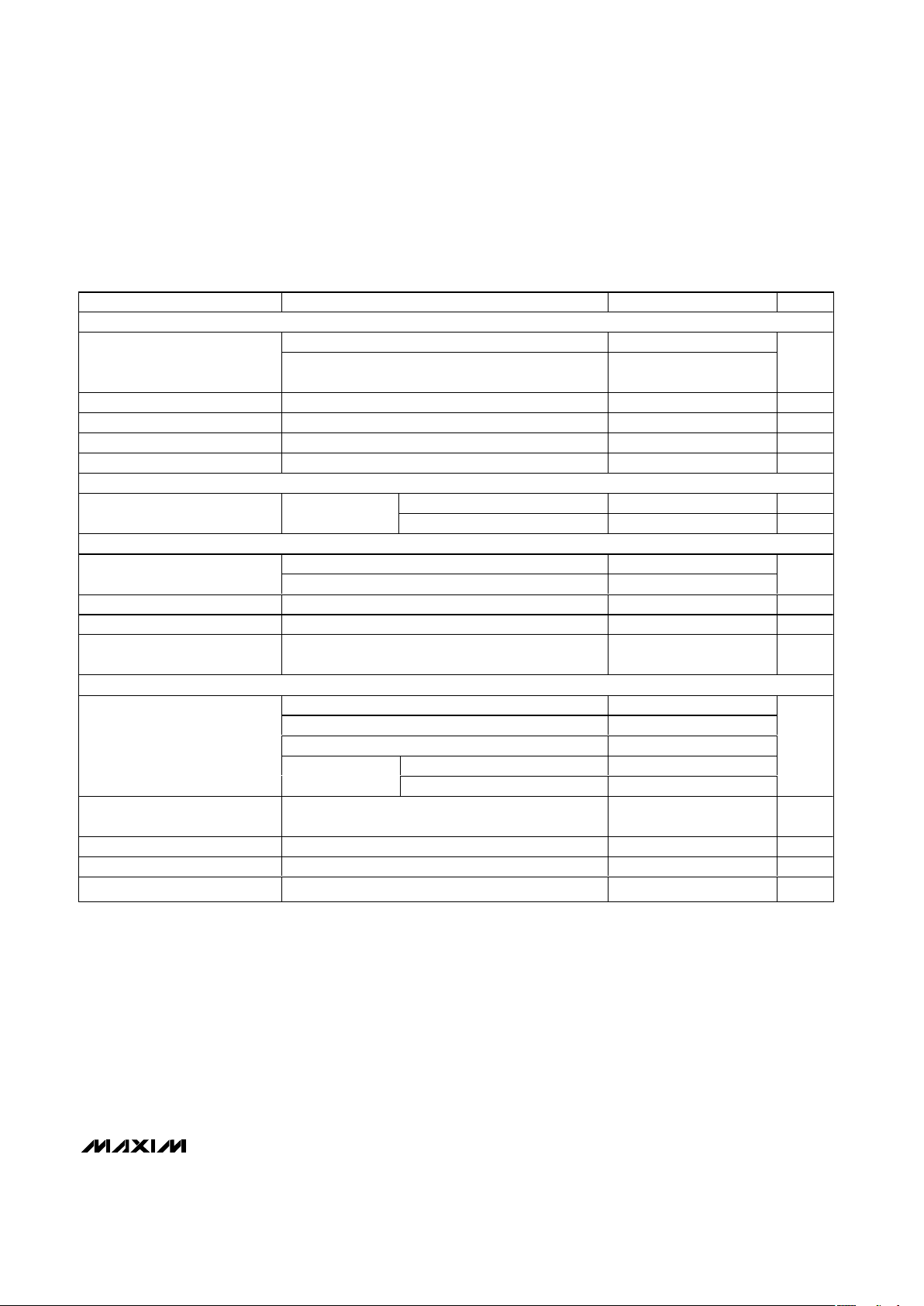
ELECTRICAL CHARACTERISTICS (continued)
(VIN= 12V, V
BST
- VLX= 6.5V, TA= -40°C to +85°C, circuit of Figure 4, typical values are at TA= +25°C, unless otherwise noted.) (Note 2)
PARAMETER CONDITIONS MIN
TYP
MAX
UNITS
ERROR AMPLIFIER
REFIN = AVL
0.693
0.7
0.707
FB Regulation Voltage
V
REFIN
= 0.7V to 1.5V
V
RE F IN
-
0.00375
V
REFIN
V
RE FIN
+
0.00375
V
Transconductance 70 110 160 µS
COMP Shutdown Resistance From COMP to GND, V
EN
= 0V 20 100 Ω
FB Input Leakage Current V
FB
= 0.7V 5 50 nA
FB Input Common-Mode Range -0.1
+1.5
V
CURRENT-SENSE AMPLIFIER
V
OUT
= 0 to 5.5V 12
V/V
Voltage Gain
V
C S +
- V
C S -
= 30m V
Part to part variation at T
A
= +85°C
-4 +4 %
CURRENT LIMIT
R
ILIM1
= 24kΩ
27.2
32
36.8
Peak Current-Limit
Threshold (V
CS+
- V
CS-
)
ILIM1 = AVL 60 80 92
mV
Negative Current Limit % of valley current limit -90
-120 -150
%
CS+, CS- Input Bias Current V
CS+
= V
CS-
= 0 or 5.5V -25 +25 µA
CS+, CS- Input Common-Mode
Range
0 5.5 V
SLOPE COMPENSATION
V
SCOMP
= 2.5V
231.25 250.00 268.75
V
SCOMP
= 1.25V
113.77 123.00 132.23
SCOMP = AVL
231.25 250.00 268.75
T
A
= 0°C to +85°C
113.77 123.00 132.23
Slope Compensation at Maximum
Duty Cycle
SCOMP = GND
T
A
= -40°C to +85°C
110.70 123.00 132.23
mV
SCOMP High Threshold
V
AVL
-
0.5
V
SCOMP Low Threshold 0.5 V
SCOMP Adjustment Range
1.25
2.50
V
SCOMP Input Leakage Current V
SCOMP
= 1.25V to 2.5V 5 200 nA
MAX8655
Highly Integrated, 25A, Wide-Input,
Internal MOSFET, Step-Down Regulator
4 _______________________________________________________________________________________
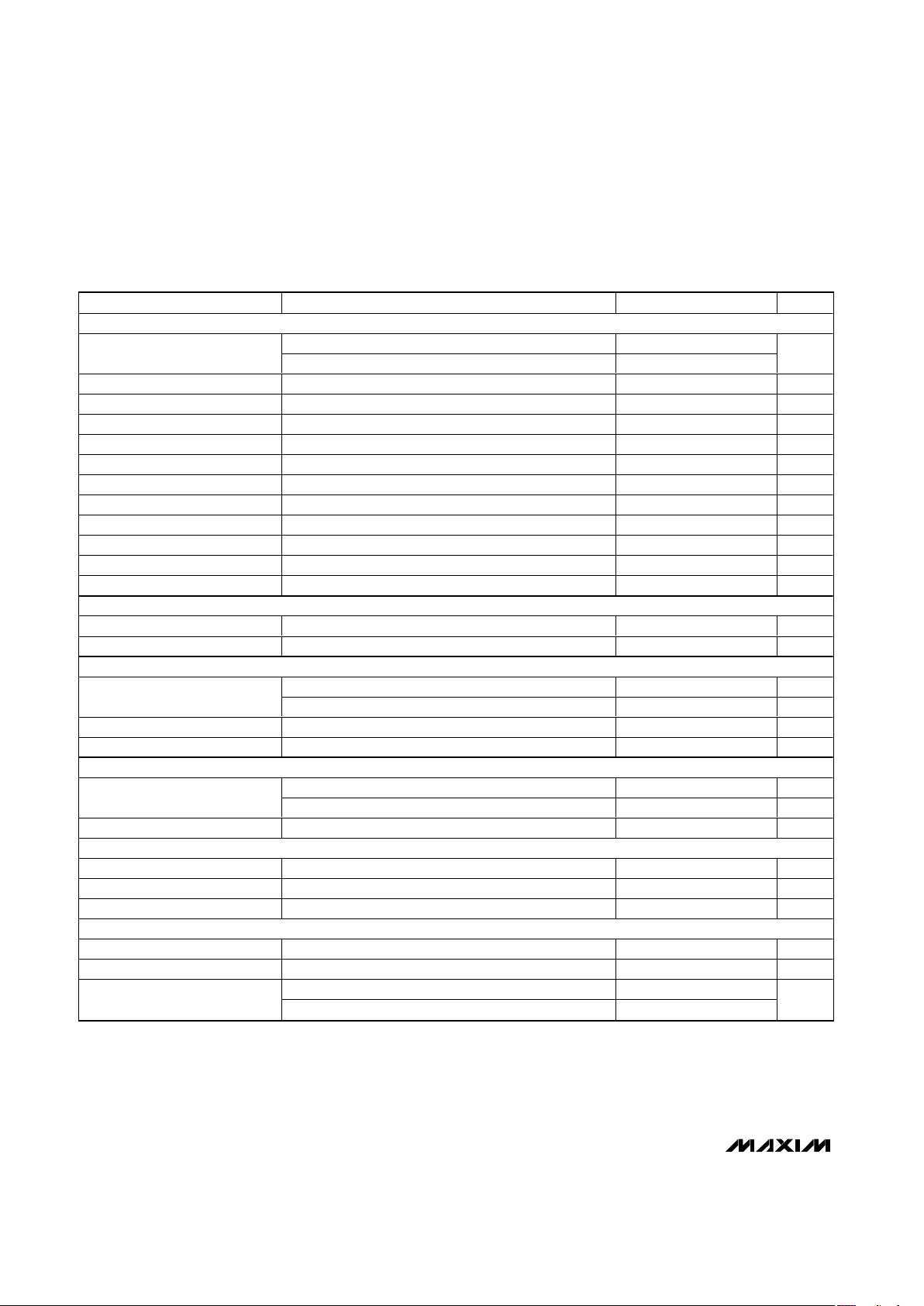
ELECTRICAL CHARACTERISTICS (continued)
(VIN= 12V, V
BST
- VLX= 6.5V, TA= -40°C to +85°C, circuit of Figure 4, typical values are at TA= +25°C, unless otherwise noted.) (Note 2)
PARAMETER CONDITIONS
MIN TYP MAX
UNITS
OSCILLATOR
R
FSYNC
= 21.0kΩ
800 1000 1200
Switching Frequency
R
FSYNC
= 143kΩ
160 200
240
kHz
Minimum Off-Time Measured at LX
235
ns
Minimum On-Time Measured at LX 75 100 ns
FSYNC Synchronization Range
160
1200
kHz
FSYNC Input High Pulse Width
100
ns
FSYNC Input Low Pulse Width
100
ns
FSYNC Rise/Fall Time 100 ns
SYNCO Phase Shift
180
D eg r ees
SYNCO Output Low Level I
SYNCO
= 5mA 0.4 V
SYNCO Output High Level I
SYNCO
= -5mA V
AV L
- 1V V
FSYNC Input Low 0.4 V
FSYNC Input High 2.5 V
THERMAL PROTECTION
Thermal Shutdown Rising temperature
+160
°C
Thermal-Shutdown Hysteresis 15 °C
POK
REFIN = AVL, V
FB
rising, typical hysteresis is 3%
629 650
671 mV
POK Threshold
V R E F IN = 0.75V to 1.5V , V F B r i si ng , typ i cal hyster esi s i s 3% 88.7 91.7 94.7
%
POK Output Voltage, Low V
FB
= 0.6V, I
POK
= 2mA
25 200 mV
POK Leakage Current, High V
POK
= 5.5V 1 µA
OVP
REFIN = AVL
770 800
840 mV
OVP Threshold Voltage
V
REFIN
= 0.7V to 1.5V
110 115
120 %
OVP, Leakage Current, High V
OVP
= 0.8V 500 nA
MODE CONTROL
MODE Logic-Level Low 4.5V ≤ V
AVL
≤ 5.5V 0.4 V
MODE Logic-Level High 4.5V ≤ V
AVL
≤ 5.5V 1.8 V
MODE Input Current V
MODE
= 0 to V
AVL
-1
+1
µA
SHUTDOWN CONTROL
EN Logic-Level Low 4.5V ≤ V
AVL
≤ 5.5V
0.45
V
EN Logic-Level High 4.5V ≤ V
AVL
≤ 5.5V 2 V
V
EN
= 0V -1
+1
EN Input Current
V
EN
= 28V 1.5 6.0
µA
Note 2: Specifications are 100% production tested at TA= +85°C. Limits over the operating temperature range are guaranteed by
design.
MAX8655
Highly Integrated, 25A, Wide-Input,
Internal MOSFET, Step-Down Regulator
_______________________________________________________________________________________ 5
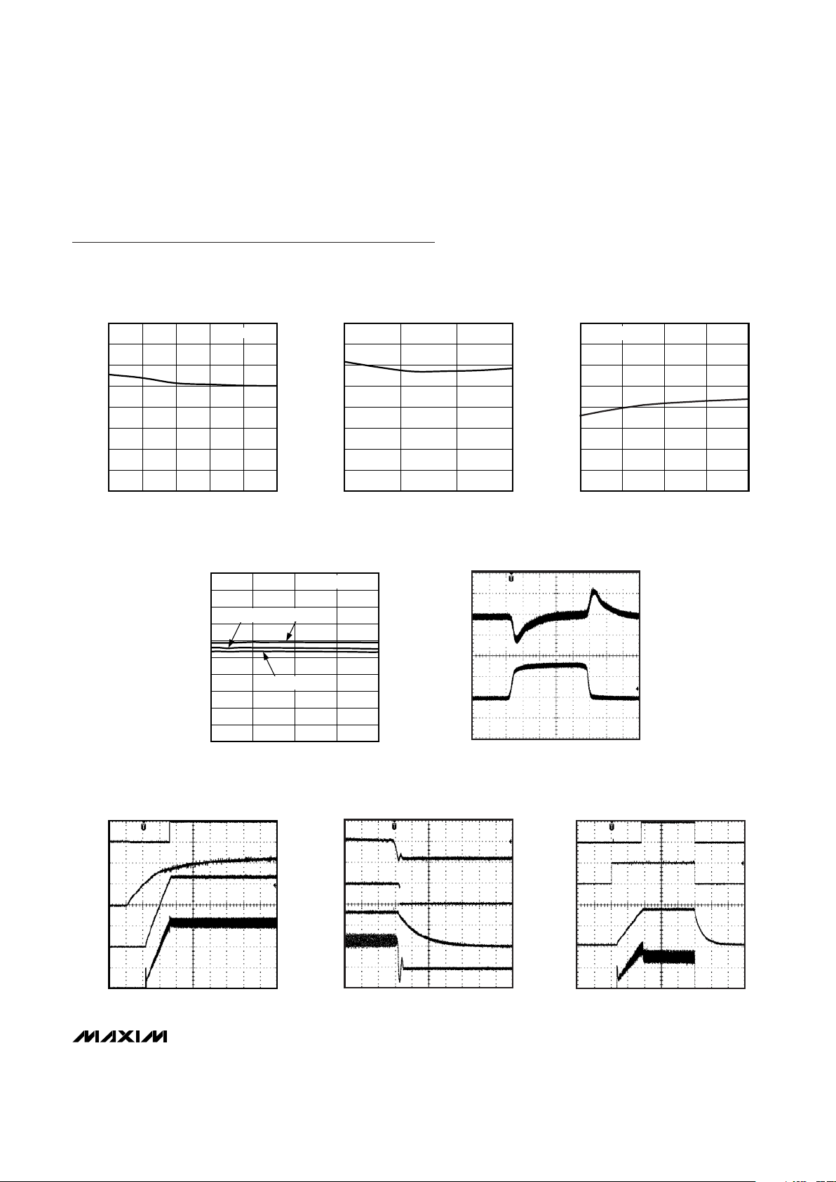
Typical Operating Characteristics
(TA = +25°C, unless otherwise noted.)
Typical Operating Characteristics
(TA = +25°C, unless otherwise noted.)
LOAD REGULATION
(CIRCUIT OF FIGURE 4)
LOAD CURRENT (A)
OUTPUT VOLTAGE (V)
MAX8655 toc01
0 5 10 15 20 25
3.26
3.27
3.28
3.29
3.30
3.31
3.32
3.33
3.34
VIN = 12V
LINE REGULATION
(CIRCUIT OF FIGURE 4)
INPUT VOLTAGE (V)
OUTPUT VOLTAGE (V)
MAX8655 toc02
5 101520
3.26
3.27
3.28
3.29
3.30
3.31
3.32
3.33
3.34
12A LOAD
FB VOLTAGE vs. EXPOSED PAD TEMPERATURE
(CIRCUIT OF FIGURE 4)
EXPOSED PAD TEMPERATURE (°C)
FB VOLTAGE (V)
MAX8655 toc03
-40 0 40 80 120
0.680
0.685
0.690
0.695
0.700
0.705
0.710
0.715
0.720
7.5A LOAD
OSCILLATOR FREQUENCY vs. INPUT VOLTAGE
(CIRCUIT OF FIGURE 4)
INPUT VOLTAGE (V)
OSCILLATOR FREQUENCY (kHz)
MAX8655 toc04
8 13182328
300
310
320
330
340
350
360
370
380
390
400
TA = -40°C
TA = +25°C
TA = +85°C
R
FSYNC
= 76.8kΩ
I
OUT
5A/div
0A
V
OUT
50mV/div
(AC-COUPLED)
40
μ
s/div
STEP-LOAD RESPONSE
(CIRCUIT OF FIGURE 3)
MAX8655 toc05
V
OUT
= 1.2V
V
IN
I
LX
10V/div
1V/div
5A/div
2ms/div
POWER-UP WAVEFORMS
(CIRCUIT OF FIGURE 4)
MAX8655 toc06
V
POK
V
OUT
5V/div
V
POK
I
LX
10V/div
2V/div
10A/div
200μs/div
POWER-DOWN WAVEFORMS
(CIRCUIT OF FIGURE 4)
MAX8655 toc07
V
IN
V
OUT
5V/div
V
EN
I
LX
5V/div
2V/div
10A/div
2ms/div
ENABLE WAVEFORMS
(CIRCUIT OF FIGURE 4)
MAX8655 toc08
V
POK
V
OUT
5V/div
MAX8655
Highly Integrated, 25A, Wide-Input,
Internal MOSFET, Step-Down Regulator
6 _______________________________________________________________________________________
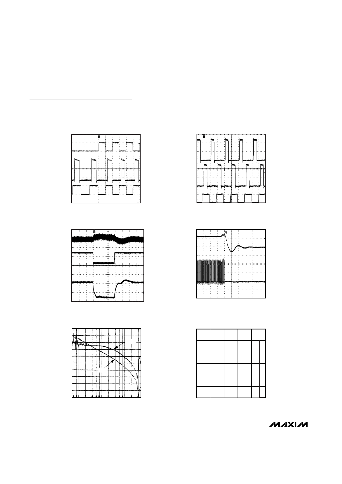
Typical Operating Characteristics (continued)
(TA = +25°C, unless otherwise noted.)
V
SYNCO
V
FSYNC
V
LX
5V/div
5V/div
5V/div
1
μ
s/div
FSYNC AND SYNCO
(CIRCUIT OF FIGURE 4)
MAX8655 toc09
INTERNAL 350kHz
OPERATION
SYNCHRONIZED TO
EXTERNAL 500kHz CLOCK
V
SYNCO
(MASTER)
V
LX
(SLAVE)
V
LX
(MASTER)
5V/div
5V/div
5V/div
1
μ
s/div
DUAL-PHASE SWITCHING
(CIRCUIT OF FIGURE 5)
MAX8655 toc10
I
IN
V
IN
V
OUT
500mV/div
(AC-COUPLED)
1V/div
1A/div
1ms/div
SHORT CIRCUIT AND RECOVERY
MAX8655 toc11
V
OUT
V
LX
2V/div
5V/div
40μs/div
OVERVOLTAGE PROTECTION
(CIRCUIT OF FIGURE 3)
MAX8655 toc12
CLOSED-LOOP BODE PLOT
(CIRCUIT OF FIGURE 3)
MAX8655toc13
50
500 1k 2k 4k 10k 20k
FREQUENCY (Hz)
GAIN (dB)
PHASE MARGIN (DEGREES)
40k 100k 200k400k
40
30
20
10
0
180
144
108
72
36
0
-10
-20
-30
-40
GAIN
PHASE
SAFE OPERATING AREA
INPUT VOLTAGE (V)
OUTPUT CURRENT (A)
MAX8655 toc14
5 1015202530
0
5
10
15
20
25
30
MAX8655
Highly Integrated, 25A, Wide-Input,
Internal MOSFET, Step-Down Regulator
_______________________________________________________________________________________ 7
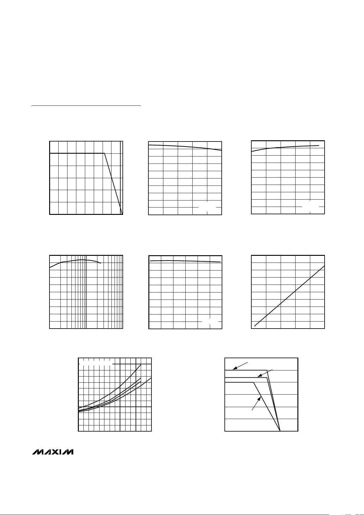
Typical Operating Characteristics (continued)
(TA= +25°C, unless otherwise noted.)
MAXIMUM OUTPUT CURRENT
vs. EXPOSED PAD TEMPERATURE
(CIRCUIT OF FIGURE 4)
EXPOSED PAD TEMPERATURE (°C)
OUTPUT CURRENT (A)
MAX8655 toc15
-40 80 10040020-20 60 120
0
5
10
15
20
25
30
EFFICIENCY vs. INPUT VOLTAGE
(CIRCUIT OF FIGURE 4)
INPUT VOLTAGE (V)
EFFICIENCY (%)
MAX8655 toc16
5 8 11 14 17 20
0
10
20
30
40
50
60
70
80
90
100
VO = 3.3V
10A LOAD
EFFICIENCY vs. OUTPUT VOLTAGE
(CIRCUIT OF FIGURE 4)
OUTPUT VOLTAGE (V)
EFFICIENCY (%)
MAX8655 toc17
1.0 1.5 2.0 2.5 3.0 3.5
0
10
20
30
40
50
60
70
80
90
100
12V INPUT
10A LOAD
EFFICIENCY vs. LOAD CURRENT
12V INPUT, 3.3V OUTPUT
(CIRCUIT OF FIGURE 4)
LOAD CURRENT (A)
EFFICIENCY (%)
MAX8655 toc18
0
10
20
30
40
50
60
70
80
90
100
1 10 100
EFFICIENCY vs. FREQUENCY
12.0V INPUT 3.3V OUTPUT
(CIRCUIT OF FIGURE 4)
FREQUENCY (kHz)
EFFICIENCY (%)
MAX8655 toc19
200 300 400 500 600 700 800
0
10
20
30
40
50
60
70
80
90
100
10A LOAD
R
VALLEY
vs. VALLEY CURRENT LIMIT
VALLEY CURRENT LIMIT (A)
R
VALLEY
(kΩ)
MAX8655 toc20
0 5 10 15 20 25
0
20
40
60
80
100
120
140
160
180
200
BOTTOM LAYER PCB TEMPERATURE vs.
OUTPUT CURRENT
I
OUT
(A)
BOTTOM PCB TEMPERATURE (°C)
MAX8655 toc21
0 5 10 15 20 25
0
120
80
20
100
40
60
VIN = 12V, VCC = 1.2V
OUTPUT-CURRENT CAPABILITY
vs. AMBIENT TEMPERATURE
AMBIENT TEMPERATURE (°C)
OUTPUT-CURRENT CAPABILITY (A)
MAX8655 toc22
-40 -25 -10 5 20 35 50 65 80 95 110 125
0
30
20
5
25
10
15
300 LFM
100 LFM
NO AIRFLOW
MAX8655
Highly Integrated, 25A, Wide-Input,
Internal MOSFET, Step-Down Regulator
8 _______________________________________________________________________________________
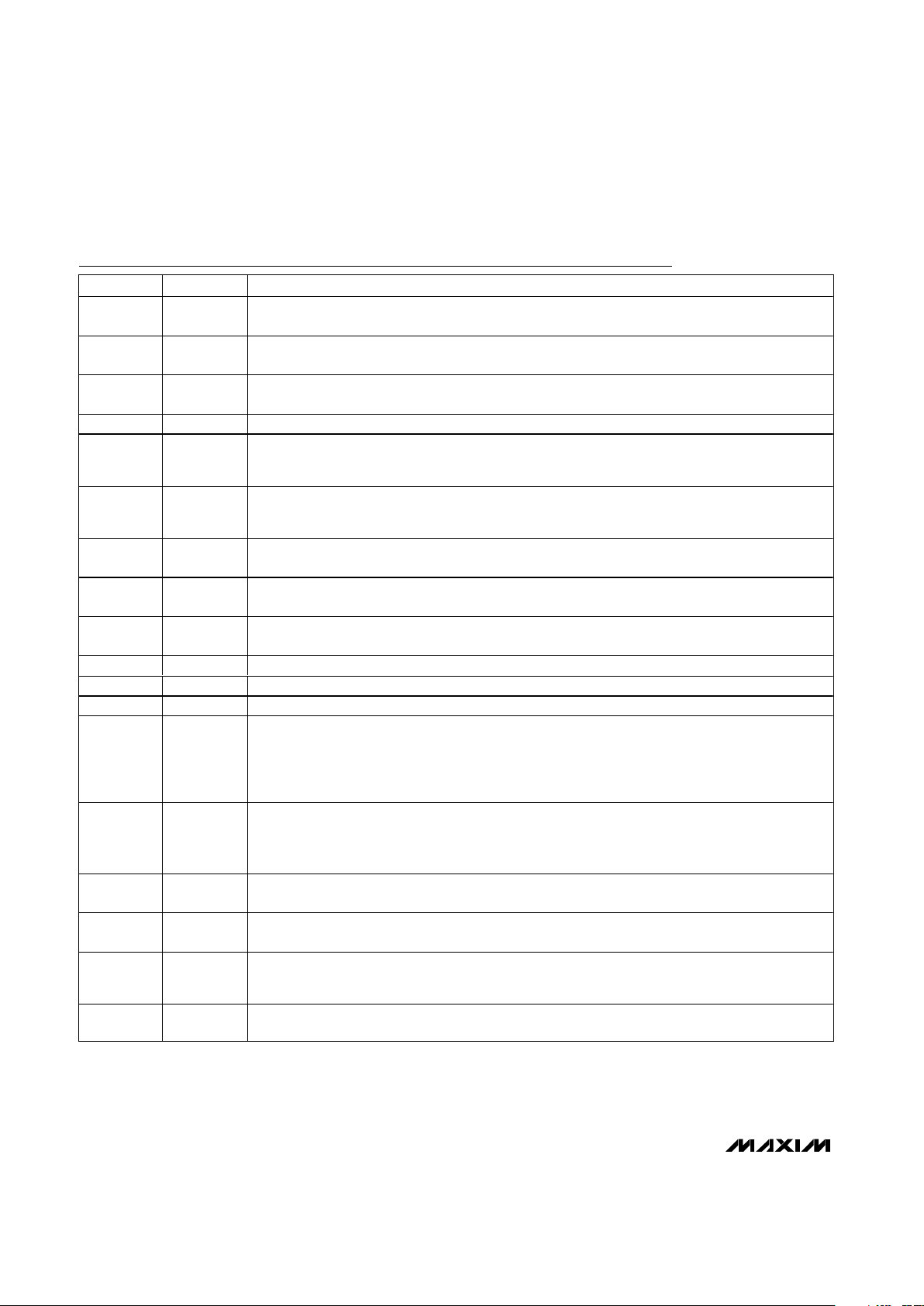
Pin Description
PIN NAME FUNCTION
1–5, 51–56
PVIN
Power-Input Supply. PVIN connects to the drain of the internal high-side MOSFET. Connect inputdecoupling capacitors as close as possible between PVIN and PGND.
6, 16–21 LX
External Inductor Connection. Connect to the external power inductor. Leave pin 6 unconnected for
best routing.
7–15 PGND
Power Ground Connection from Source of Internal Low-Side MOSFET. Connect input-decoupling
capacitors as close as possible between PVIN and PGND.
22 VLGND Return for Low-Side MOSFET Gate-Driver Current
23, 28, 39,
48
GND
Analog Ground. Connect all pins to the analog ground plane, and connect the analog and power
ground planes together at the negative terminal of the output capacitor. Low-current signals return to
GND. Pin 28 must be connected externally to GND-EP, the analog ground plane.
24 VL
Internal 6.5V Linear-Regulator Output. Connect a 2.2µF to 10µF ceramic capacitor from VL to VLGND.
For V
IN
< 7V, connect VL directly to IN. VL supplies power for the internal gate drivers. VL is the input
to the AVL internal linear regulator.
25 IN
Input Supply Voltage. IN is the input to the VL linear regulator. Connect VL to IN for V
IN
< 7V.
Decouple to PGND with a 0.22µF ceramic capacitor.
26 EN
Enable. Apply logic-high to EN to enable the output, or logic-low to place the regulator in low-power
shutdown mode. Connect EN to IN for always-on operation.
27 AVL
Internal 5V Linear-Regulator Output. AVL powers the MAX8655’s internal circuits. Connect a 1µF
ceramic capacitor from AVL to GND.
29, 30, 42, 49
N.C. No Connection. Not internally connected.
31 CS+ Positive Differential Current-Sense Input
32 CS- Negative Differential Current-Sense Input
33 ILIM1
Analog Programmable Current-Limit Input for Inductor Current. Connect a resistor from ILIM1 to GND
to set the overcurrent threshold. ILIM1 sources 10µA through the resistor, and the voltage at ILIM1 is
attenuated 7.5:1 to set the final current limit. For example, a 60kΩ resistor results in 600mV at ILIM1.
This results in a current-limit threshold (V
CS+
- V
CS-
) of 80mV. The ILIM1 resistor range is 24kΩ to
60kΩ. Connect ILIM1 to AVL to set the default threshold of 80mV.
34 OVP
Output-Voltage Sensing for Overvoltage Protection. Connect OVP to the center of a resistor-divider
connected between the output of the regulator and GND to set the FB independent output
overvoltage trip point. Connect OVP to FB if this independence is not desired. The OVP threshold is
1.15 times the nominal feedback regulation voltage.
35 FB
Feedback Input. Connect FB to the center of a resistor voltage-divider connected between the output
and GND to set the output voltage. FB regulates to 0.7V or V
REFIN
.
36 COMP
Loop Compensation. Connect COMP to an external RC network to compensate the loop. COMP is
internally pulled to GND through 20Ω during shutdown.
37 SS
Soft-Start. Connect a 0.01µF to 1µF ceramic capacitor from SS to GND. This capacitor sets the softstart period during startup. See the Startup and Soft-Start section for more details. SS is internally
pulled to GND through 20Ω during shutdown.
38 REFIN
External Reference Input. Connect REFIN to AVL to use the internal 0.7V reference for the feedback
threshold.
 Loading...