Maxim MAX863C-D, MAX863EEE Datasheet
_______________General Description
The MAX863 dual-output DC-DC converter contains
two independent step-up controllers in a single compact package. This monolithic bi-CMOS design draws
only 85µA when both controllers are on. The input
range extends down to 1.5V, permitting use in organizers, translators, and other low-power hand-held products. The MAX863 provides 90% efficiency at output
loads from 20mA to over 1A. This space-saving device
is supplied in a 16-pin QSOP package that fits in the
same area as an 8-pin SOIC.
The device uses a current-limited, pulse-frequencymodulated (PFM) control architecture that reduces startup surge currents and maintains low quiescent currents
for excellent low-current efficiency. Each controller
drives a low-cost, external, N-channel MOSFET switch,
whose size can be optimized for any output current or
voltage.
In larger systems, two MAX863s can be used to generate 5V, 3.3V, 12V, and 28V from just two or three battery cells. An evaluation kit (MAX863EVKIT) is available
to speed designs. For a single-output controller, refer to
the MAX608 and MAX1771 data sheets.
________________________Applications
2- and 3-Cell Portable Equipment
Organizers
Translators
Hand-Held Instruments
Palmtop Computers
Personal Digital Assistants (PDAs)
Dual Supply (Logic and LCD)
____________________________Features
♦ Smallest Dual Step-Up Converter: 16-Pin QSOP
♦ 90% Efficiency
♦ 1.5V Start-Up Voltage
♦ 85µA Max Total Quiescent Supply Current
♦ 1µA Shutdown Mode
♦ Independent Shutdown Inputs
♦ Drives Surface-Mount, Dual N-Channel MOSFETs
♦ Low-Battery Input/Output Comparator
♦ Step-Up/Down Configurable
MAX863
Dual, High-Efficiency, PFM, Step-Up
DC-DC Controller
________________________________________________________________
Maxim Integrated Products
1
MAX863
EXT2
CS2
OUT2
OUT1
V
IN
N
N
ON/OFF
FB2
SHDN1
EXT1
CS1
LBO
LOW-BATTERY
DETECTOR OUTPUT
LBI
SENSE1 V
DD
PGND
BOOT
GND
FB1
SHDN2
REF
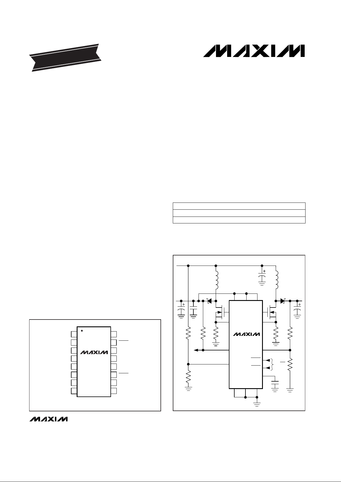
__________________Pin Configuration
16
15
14
13
12
11
10
9
1
2
3
4
5
6
7
8
SENSE1 REF
SHDN2
LBI
LBO
FB2
SHDN1
CS2
EXT2
TOP VIEW
MAX863
QSOP
V
DD
FB1
EXT1
BOOT
CS1
GND
PGND
__________Typical Operating Circuit
19-1218; Rev 1; 6/97
PART
MAX863C/D
MAX863EEE -40°C to +85°C
0°C to +70°C
TEMP. RANGE PIN-PACKAGE
Dice*
16 QSOP
EVALUATION KIT MANUAL
AVAILABLE
______________Ordering Information
For free samples & the latest literature: http://www.maxim-ic.com, or phone 1-800-998-8800
*
Dice are tested at TA= +25°C.
MAX863
Dual, High-Efficiency, PFM, Step-Up
DC-DC Controller
2 _______________________________________________________________________________________
ABSOLUTE MAXIMUM RATINGS
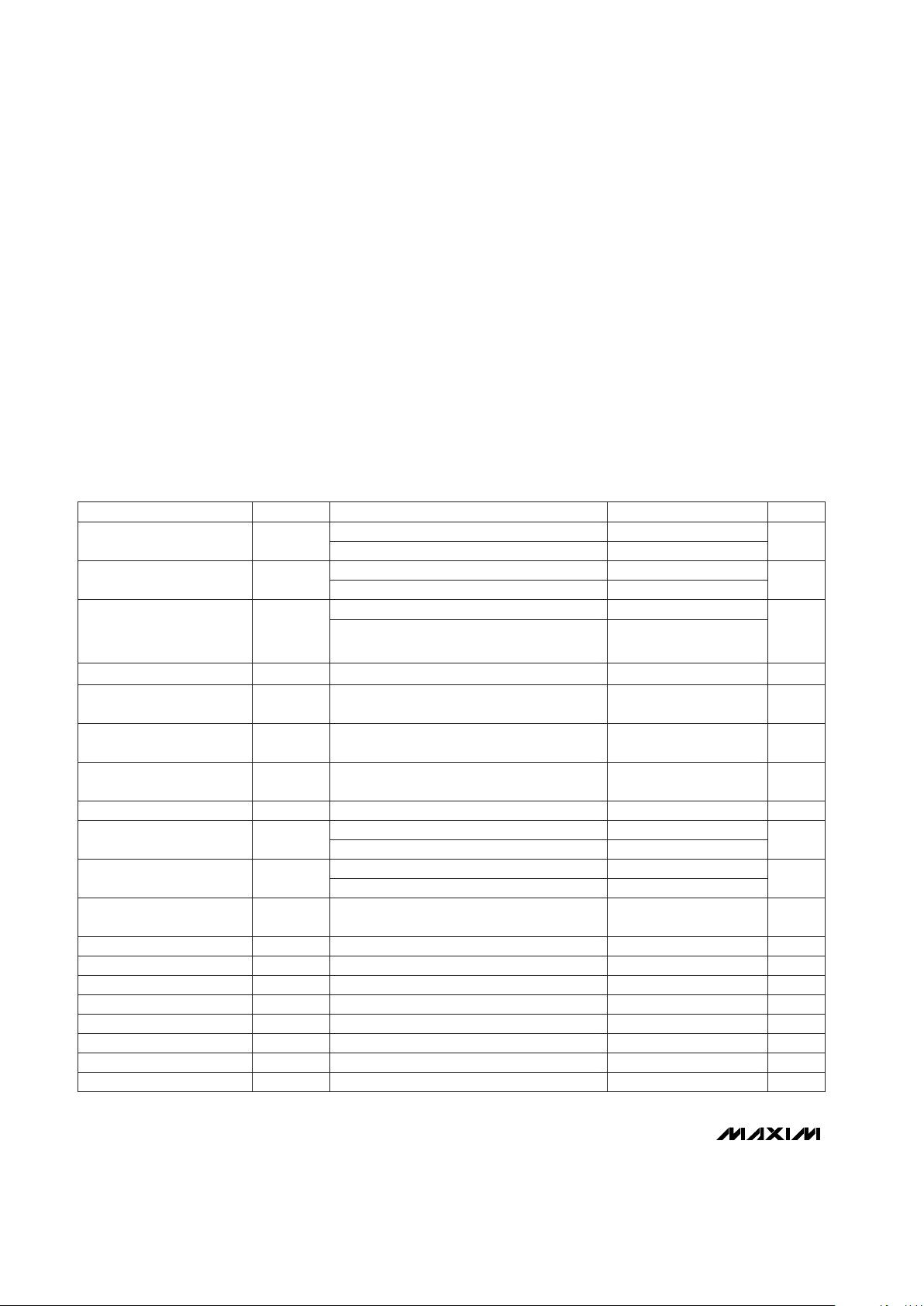
ELECTRICAL CHARACTERISTICS
(VDD= +5V, I
LOAD
= 0mA, TA= 0°C to +85°C, unless otherwise noted. Typical values are at TA= +25°C.)
Stresses beyond those listed under “Absolute Maximum Ratings” may cause permanent damage to the device. These are stress ratings only, and functional
operation of the device at these or any other conditions beyond those indicated in the operational sections of the specifications is not implied. Exposure to
absolute maximum rating conditions for extended periods may affect device reliability.
VDDto GND............................................................-0.3V to +12V
PGND to GND .......................................................-0.3V to +0.3V
SHDN1, SHDN2, SENSE1, LBO to GND................-0.3V to +12V
EXT1, EXT2 to PGND..................................-0.3V to (V
DD
+ 0.3V)
FB1, FB2, CS1, CS2, SEL,
LBI, BOOT to GND.................................-0.3V to (V
DD
+ 0.3V)
LBO Continuous Output Current.........................................15mA
EXT1, EXT2 Continuous Output Current.............................50mA
Continuous Power Dissipation (T
A
= +70°C)
QSOP (derate 8.30mW/°C above +70°C) ...................667mW
Operating Temperature Range
MAX863EEE ....................................................-40°C to +85°C
Junction Temperature......................................................+150°C
Storage Temperature Range.............................-65°C to +160°C
Lead Temperature (soldering, 10sec).............................+300°C
V
DD
= OUT1 = BOOT (Note 1)
CONDITIONS
1.5 11
UNITSMIN TYP MAXSYMBOLPARAMETER
(Note 2)
V
2.7 11
V
DD
VDDInput Voltage
SHDN1 = VDD, SHDN2 = GND,
measured from V
DD
µA
35 60
I
DD
Quiescent Current
SHDN1 = SHDN2 = VDD, measured from V
DD
50 85
VIN= 2.7V to 5V, V
OUT1
= 5V,
I
LOAD
= 300mA, Figure 2
mV/V8Line Regulation
VIN= 3.3V, V
OUT1
= 5V,
I
LOAD
= 0mA to 500mA, Figure 2
mV/A40Load Regulation
nA2 10IFB, I
LBI
FB1, FB2, LBI Input Current
VDD= 1.5V
V
0.7 x V
DD
V
IH
2.7V < VDD< 11V 1.6
SHDN1, SHDN2, SEL, BOOT
Input High Voltage
mV85 100 115V
CS
CS1, CS2 Threshold Voltage
µs14 17.5 22
Logic input = VDDor GND
t
ON
Maximum Switch On-Time
µA1 25CS1, CS2 Input Current
µA1I
I
SHDN1, SHDN2, SEL, BOOT
Input Current
V1.225 1.25 1.275VFB, V
LBI
FB1, FB2, LBI
Threshold Voltage (Note 4)
C
LOAD
= 1nF, 10% to 90% ns50EXT Rise/Fall Time (Note 5)
µs1.6 2 2.4t
OFF
Minimum Switch Off-Time
FB1 = GND
V
4.85 5 5.15
V
OUT1
OUT1 Output Voltage
(Note 3)
FB1 = V
DD
3.2 3.3 3.4
VDD= 1.5V
V
0.2 x V
DD
V
IL
2.7V < VDD< 11V 0.4
SHDN1, SHDN2, SEL, BOOT
Input Low Voltage
SHDN1 = SHDN2 = GND
µA1I
DD, SHDN
Shutdown Current
Ω
5EXT On-Resistance
V
LBO
= 11V, V
LBI
> 1.275V µA1I
LBO
LBO Leakage Current
I
LBO,SINK
= 1mA, V
LBI
< 1.225V V0.1 0.4V
LBO,L
LBO Low Level
MAX863
Dual, High-Efficiency, PFM, Step-Up
DC-DC Controller
_______________________________________________________________________________________ 3
ELECTRICAL CHARACTERISTICS
(VDD= +5V, I
LOAD
= 0mA, TA= 0°C to +85°C, unless otherwise noted.) (Note 6)
Note 1: When bootstrapped, an internal low-voltage oscillator drives the EXT1 pin rail-to-rail for low supply voltages.
Note 2: For non-bootstrapped operation, V
DD
> 2.7V is required to allow valid operation of all internal circuitry.
Note 3: For adjustable output voltages, see the
Set the Output Voltage
section.
Note 4: Measured with LBI falling. Typical hysteresis is 15mV.
Note 5: EXT1 and EXT2 swing from V
DD
to GND.
Note 6: Specifications to -40°C are guaranteed by design and not production tested.
VDD= OUT1 (Note 1) 1.6 11
CONDITIONS
VDDInput Voltage
(Note 2)
V
2.8 11
V
DD
V1.21 1.285V
FB
FB1, FB2 Threshold Voltage
60
mV85 115V
CS
CS1, CS2 Threshold Voltage
UNITSMIN TYP MAXSYMBOLPARAMETER
FB1 = V
DD
3.15 3.45
OUT1 Output Voltage
(Note 3)
FB1 = GND
V
4.8 5.2
V
OUT1
SHDN1 = SHDN2 = VDD, measured from V
DD
85
Quiescent Current
SHDN1 = VDD, SHDN2 = GND,
measured from V
DD
µAI
DD
SHDN1 = SHDN2 = GND
µA1I
DD, SHDN
Shutdown Current
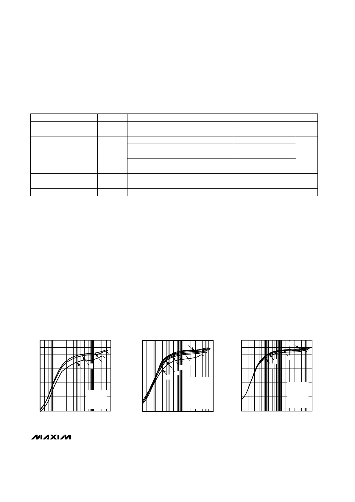
__________________________________________Typical Operating Characteristics
(TA = +25°C, unless otherwise noted.)
0.01 0.1 1 10 100 1000
EFFICIENCY vs. OUTPUT CURRENT
(V
OUT1
= 3.3V, BOOTSTRAPPED)
MAX863 toc01
OUTPUT CURRENT (mA)
EFFICIENCY (%)
B
C
A
10
0
30
20
50
40
70
60
90
80
100
V
OUT1
= 3.3V
A: V
IN
= 1.5V
B: V
IN
= 2.4V
C: V
IN
= 2.7V
0.01 0.1
10
0
30
20
50
40
70
60
90
80
100
1 10 100 1000
EFFICIENCY vs. OUTPUT CURRENT
(V
OUT1
= 5.0V, BOOTSTRAPPED)
MAX863 toc02
OUTPUT CURRENT (mA)
EFFICIENCY (%)
V
OUT1
= 5.0V
A: V
IN
= 1.5V
B: V
IN
= 2.4V
C: V
IN
= 2.7V
D: V
IN
= 3.3V
E: V
IN
= 3.6V
F: V
IN
= 4.0V
B
C
A
D
E
F
0.01 0.1
0
10
20
30
40
50
60
70
80
90
100
1 10 100 1000
EFFICIENCY vs. OUTPUT CURRENT
(V
OUT1
= 5.0V, NON-BOOTSTRAPPED)
MAX863 toc03
OUTPUT CURRENT (mA)
EFFICIENCY (%)
V
OUT1
= 5.0V
A: V
IN
= 2.7V
B: V
IN
= 3.3V
C: V
IN
= 3.6V
D: V
IN
= 4.0V
A
B
C
D
MAX863
Dual, High-Efficiency, PFM, Step-Up
DC-DC Controller
4 _______________________________________________________________________________________
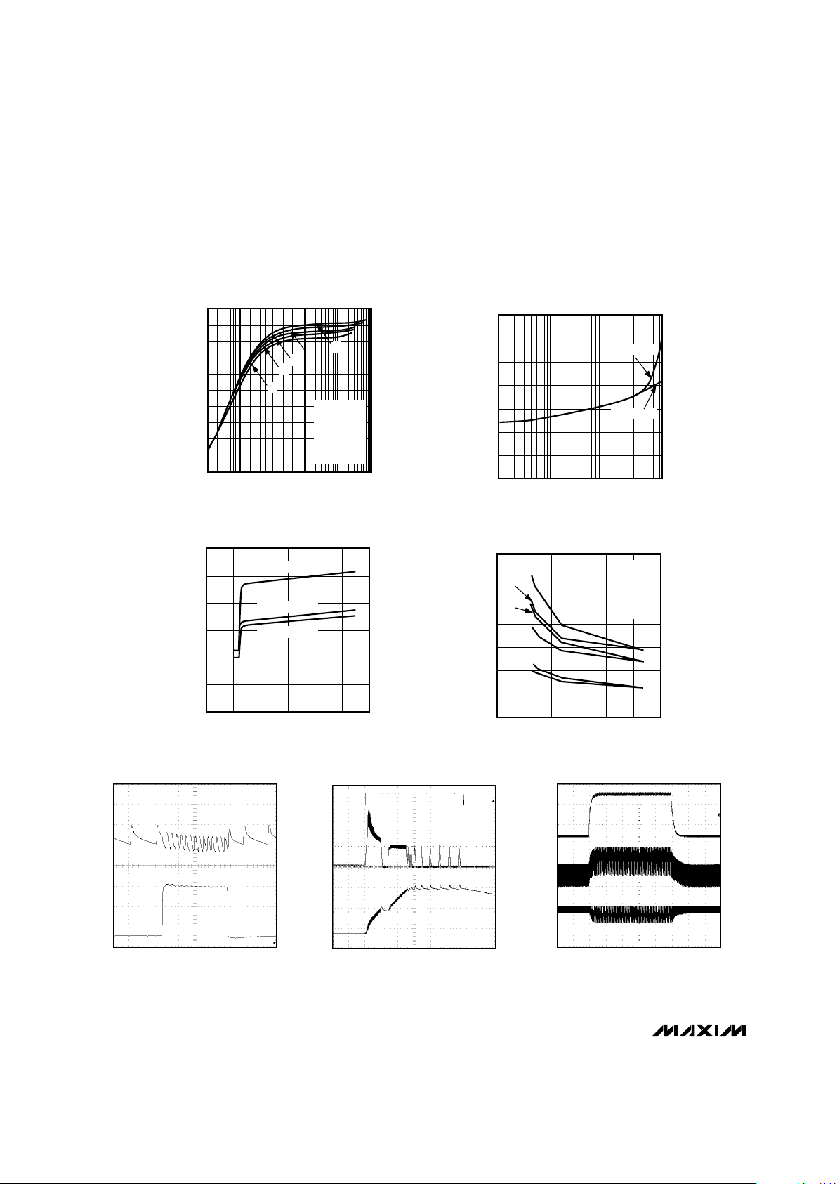
____________________________Typical Operating Characteristics (continued)
(TA = +25°C, unless otherwise noted.)
0.01 0.1
10
20
30
40
50
60
70
80
90
100
0
1 10 100 1000
EFFICIENCY vs. OUTPUT CURRENT
(V
OUT1
= 12V, NON-BOOTSTRAPPED)
MAX863 toc04
OUTPUT CURRENT (mA)
EFFICIENCY (%)
V
OUT1
= 5.0V
A: V
IN
= 2.7V
B: V
IN
= 3.3V
C: V
IN
= 3.6V
D: V
IN
= 4.0V
E: V
IN
= 6.0V
A
B
C
D
E
3.5
1
1 10 1000
BOOTSTRAPPED-MODE MINIMUM
START-UP INPUT VOLTAGE
vs. OUTPUT CURRENT
0.5
1.0
1.5
2.0
2.5
3.0
MAX863toc05
OUTPUT CURRENT (mA)
START-UP INPUT VOLTAGE (V)
100
V
OUT1
= 3.3V
V
OUT1
= 5V
0
0 12
VDD CURRENT
vs. V
DD
VOLTAGE
10
20
60
MAX863 toc15
VDD VOLTAGE (V)
V
DD
CURRENT (µA)
40
30
8
50
10
2 4 6
Cond: Single +5V
BOTH ON
CONVERTER 1 ON
CONVERTER 2 ON
LOAD-TRANSIENT RESPONSE
A
MAX863 toc08
B
100µs/div
V
OUT1
= 3.3V, I
OUT1
= 100mA TO 600mA
A: V
OUT1
, 100mV/div, 3.3V DC OFFSET
B: I
OUT1
, 200mA/div
RESPONSE ENTERING/
EXITING SHUTDOWN (BOOTSTRAPPED)
B
A
MAX863 toc09
C 3.3V
200µs/div
V
OUT1
= 3.3V, I
OUT1
= 100mA, VIN = 2.4V
A: SHDN1, 5V/div
B: INDUCTOR CURRENT, 2A/div
C: V
OUT1
, 3.3V OFFSET, 500mV/div
LINE-TRANSIENT RESPONSE
B
A
MAX863 toc10
C 0A
500µs/div
V
OUT1
= 5V, I
OUT1
= 800mA
A: V
IN
= 2.7V TO 3.7V, 500mV/div
B: V
OUT1
, AC COUPLED, 50mV/div
C: INDUCTOR CURRENT, 2A/div
0
0 12
EXT RISE AND FALL TIMES vs.
SUPPLY VOLTAGE AND MOSFET CAPACITANCE
20
140
MAX863 toc07
SUPPLY VOLTAGE (V)
RISE/FALL TIME (ns)
6
60
80
40
2 4 8
120
100
C,1
C,2
B,1
B,2
A,1
A,2
10
A: 470pF
B: 1.0nF
C: 2.2nF
1: RISE
2: FALL
MAX863
Dual, High-Efficiency, PFM, Step-Up
DC-DC Controller
_______________________________________________________________________________________ 5
_______________Detailed Description
The MAX863 dual, bi-CMOS, step-up, switch-mode
power-supply controller provides preset 3.3V, 5V, or
adjustable outputs. Its pulse-frequency-modulated
(PFM) control scheme combines the advantages of low
supply current at light loads and high efficiency with
heavy loads. These attributes make the MAX863 ideal
for use in portable battery-powered systems where
small size and low cost are extremely important, and
where low quiescent current and high efficiency are
needed to maximize operational battery life. Use of
external current-sense resistors and MOSFETs allows
the designer to tailor the output current and voltage
capability for a diverse range of applications.
PFM Control Scheme
Each DC-DC controller in the MAX863 uses a one-shotsequenced, current-limited PFM design, as shown in
Figure 1. Referring to the Typical Operating Circuit
(Figure 2) and the switching waveforms (Figures 3a–3f),
the circuit works as follows. Output voltage is sensed
by the error comparator using either an internal voltage
divider connected to SENSE1 or an external voltage
divider connected to FB1. When the output voltage
drops, the error comparator sets an internal flip-flop.
The flip-flop turns on an external MOSFET, which allows
inductor current to ramp-up, storing energy in a magnetic field.
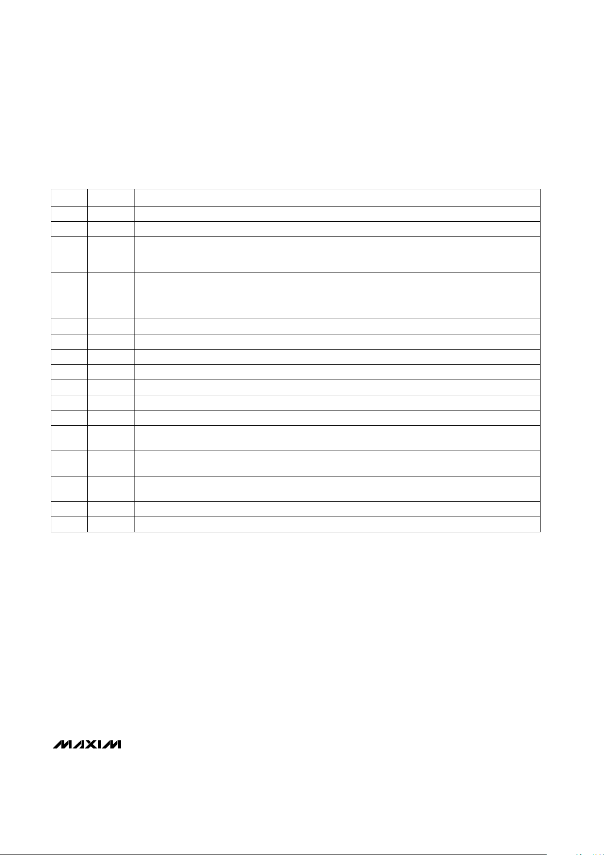
______________________________________________________________Pin Description
PIN
Feedback Input for DC-DC Controller 1 in Fixed-Output ModeSENSE11
FUNCTIONNAME
IC Power-Supply InputV
DD
2
Bootstrap Low-Voltage-Oscillator Enable Input. BOOT is an active-high, logic-level input. It enables the
low-voltage oscillator to allow start-up from input voltages down to 1.5V while in a bootstrapped circuit
configuration. Connect BOOT to GND when in a non-bootstrapped configuration. If BOOT is high, V
DD
must be connected to OUT1.
BOOT4
Adjustable Feedback and Preset Output Voltage Selection Input for DC-DC Controller 1. Connect to V
DD
for 3.3V preset output or to GND for 5V output. Connect a resistor voltage divider to adjust the output voltage. See the section
Set the Output Voltage
.
FB13
Gate-Drive Output of DC-DC Controller 1. Drives an external N-channel power MOSFET.EXT16
High-Current Ground Return for Internal MOSFET DriversPGND8
Analog Ground for Internal Reference, Feedback, and Control CircuitsGND7
Input to the Current-Sense Comparator of DC-DC Controller 1CS15
Input to the Current-Sense Amplifier of DC-DC Controller 2CS210
Adjustable Feedback Input for DC-DC Controller 2. Connect a resistor voltage divider to adjust the output
voltage. See the section
Set the Output Voltage.
FB212
Active-Low Shutdown Input for DC-DC Controller 1. Connect to VDDfor normal operation.
SHDN1
11
Low-Battery Comparator Input. When the voltage on LBI drops below 1.25V, LBO sinks current. If unused,
connect to GND.
LBI14
Reference Bypass Input. Connect a 0.1µF ceramic capacitor from REF to GND.REF16
Active-Low Shutdown Input for DC-DC Controller 2. Connect to VDDfor normal operation.
SHDN2
15
Low-Battery Output. An open-drain N-channel MOSFET output. Sinks current when the voltage on LBI
drops below 1.25V. If unused, connect to GND.
LBO13
Gate-Drive Output of DC-DC Controller 2. Drives an external N-channel power MOSFET.EXT29
 Loading...