

Page 1
General Description
The MAX8600/MAX8601 single-/dual-input linear battery chargers safely charge single-cell Li+ batteries.
The charging rate is optimized to accommodate the
thermal characteristics of a given application. There is
no need to reduce the maximum charge current or
worst-case charger power dissipation. Charging is optimized for Li+ cells using a control algorithm that
includes low-battery precharging, voltage and currentlimited fast-charging, and top-off charging, while continuously monitoring the battery for overvoltage,
over/undertemperature, and charging time. The charger timeout protection is programmable. The charger
status is indicated by three open-drain outputs.
The MAX8601 automatically selects between either a
USB or AC adapter input source. The AC adapter
charge current is programmable, while USB charge
current is set not to exceed either 100mA or 500mA,
depending on the USEL input. The MAX8600 is a single-input charger with no USB source input.
The MAX8600/MAX8601 are available in the tiny 3mm x
3mm power-enhanced TDFN package.
Applications
Cell Phones Portable Media Players
Digital Cameras MP3 Players
PDAs Wireless Appliances
Features
♦ Single- (MAX8600) or Dual- (MAX8601) Input Li+
Charger
♦ Up to 1A Programmable Fast-Charge
♦ 100mA/500mA USB Select Input (MAX8601)
♦ ±5% Fast-Charge Current-Limit Accuracy
♦ 14V Input Overvoltage Protection
♦ Programmable On-Chip Charge Timers
♦ Battery Thermistor Input
♦ Charger-Status Outputs
♦ Thermally Optimized Charge Rate
♦ 14-Pin 3mm x 3mm TDFN Package
MAX8600/MAX8601
Single-/Dual-Input 1-Cell Li+ Chargers with
OVP Protection and Programmable Charge Timer
________________________________________________________________ Maxim Integrated Products 1
19-3565; Rev 2; 7/08
For pricing, delivery, and ordering information, please contact Maxim Direct at 1-888-629-4642,
or visit Maxim’s website at www.maxim-ic.com.
EVALUATION KIT
AVAILABLE
Ordering Information
PART
TEMP
PIN-PACKAGE
TOP
PKG
CODE
MAX8600ETD
-40°C to
T1433-2
MAX8601ETD
-40°C to
T1433-2
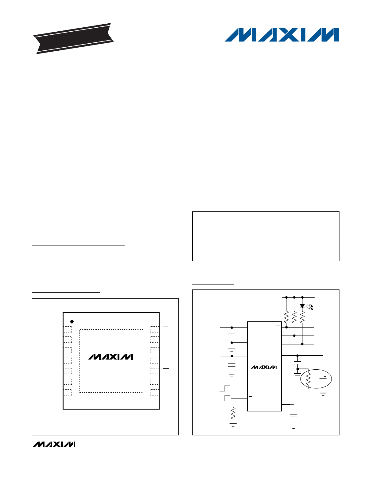
Pin Configurations continued at end of data sheet.
BAT
Li+
CT
THM
AC
ADAPTER
USB
PORT
GND
USB
EN
OFF
ON
FLT
+5V
CHARGE
STATUS
DC
SETI
USEL
POK
CHG
MAX8601
500mA
100mA
Typical Operating Circuit
8
9
10
11
12
13
14
7
6
5
4
3
2
1
MAX8600
TDFN
TOP VIEW
SETI
BAT
THM
GND
CT
N.C.
N.C.
FLT
DC
DC
CHG
POK
N.C.
EN
Pin Configurations
*EP = Exposed pad.
RANGE
+85°C
+85°C
14 TDFN-EP* 3mm
x 3mm (T1433-2)
14 TDFN-EP* 3mm
x 3mm (T1433-2)
MARK
ABB
AAC
Page 2
MAX8600/MAX8601
Single-/Dual-Input 1-Cell Li+ Chargers with
OVP Protection and Programmable Charge Timer
2 _______________________________________________________________________________________
ABSOLUTE MAXIMUM RATINGS
Stresses beyond those listed under “Absolute Maximum Ratings” may cause permanent damage to the device. These are stress ratings only, and functional
operation of the device at these or any other conditions beyond those indicated in the operational sections of the specifications is not implied. Exposure to
absolute maximum rating conditions for extended periods may affect device reliability.
DC, USB to GND ....................................................-0.3V to +16V
BAT, CT,
CHG, EN, FLT, SETI,
POK, THM, USEL to GND..................................-0.3V to +6.0V
Continuous Power Dissipation (T
A
= +70°C)
14-Pin TDFN 3mm x 3mm (derate 18.2mW/°C
above +70°C)............................................................ 1454mW
Operating Temperature Range ...........................-40°C to +85°C
Junction Temperature......................................................+150°C
Storage Temperature Range .............................-65°C to +150°C
Lead Temperature (soldering, 10s) .................................+300°C
ELECTRICAL CHARACTERISTICS
(VDC= V
USB
= 5V, V
BAT
= 4V, VEN= 0V, R
SETI
= 2kΩ, CCT= 0.068µF, TA= -40°C to +85°C, unless otherwise noted. Typical values
are at T
A
= +25°C. Note 1)
PARAMETER CONDITIONS
DC OR USB (Note 2)
Input Voltage Range 014V
Input Operating Range (Note 3)
V
Input Undervoltage Threshold
Input rising, 500mV hysteresis (typ)
4.0
V
Input Overvoltage Threshold Input rising, 200mV hysteresis (typ) 7.2 7.5 7.8 V
Input Overvoltage Delay From overvoltage event to charger disabled
s
Input Supply Current I
BAT
= 0mA, R
THM
= 10kΩ
µA
Shutdown Input Current VEN = 5V, TA = +25°C
µA
Input to BAT On-Resistance Input = 3.7V, V
BAT
= 3.6V 0.5 0.8 Ω
Input to BAT Dropout Voltage
Input falling, 200mV hysteresis (typ) 5 55
mV
BAT
TA = +25°C
4.2
BAT Regulation Voltage I
BAT
= 0mA
T
A
= -40°C to +85°C
4.2
V
BAT Restart Fast-Charge
Threshold
From BAT regulation voltage
mV
R
SETI
= 1.5kΩ
R
SETI
= 2kΩ
R
SETI
= 5kΩ
DC Charging Current V
USB
= 0V
Prequal, R
SETI
= 2kΩ, V
BAT
= 2.5V 60 75 90
mA
V
USEL
= 5V
V
USEL
= 0V 80 95
USB Charging Current VDC = 0V
Prequal, R
SETI
= 2kΩ, V
BAT
= 2.5V 60 75 90
mA
Soft-Start Time Ramp time to fast-charge current 1.2 ms
BAT Prequal Threshold V
BAT
rising, 180mV hysteresis (typ) 2.9 3 3.1 V
BAT Leakage Current VDC = V
USB
= 0V, V
BAT
= 4.2V
5µA
SETI
R
SETI
Resistance Range (Note 4) 1.5 5.0 kΩ
MIN TYP MAX UNITS
4.15 7.00
3.85
0.25
750 1200
275 435
4.179
4.166
-180 -150 -120
950 1000 1050
727 750 773
280 300 320
450 475 500
0.001
4.15
120
4.221
4.234
100
Page 3
MAX8600/MAX8601
Single-/Dual-Input 1-Cell Li+ Chargers with
OVP Protection and Programmable Charge Timer
_______________________________________________________________________________________ 3
ELECTRICAL CHARACTERISTICS (continued)
(VDC= V
USB
= 5V, V
BAT
= 4V, VEN= 0V, R
SETI
= 2kΩ, CCT= 0.068µF, TA= -40°C to +85°C, unless otherwise noted. Typical values
are at T
A
= +25°C. Note 1)
PARAMETER CONDITIONS
MIN
TYP
MAX
UNITS
EN, USEL
Rising 1.6
Logic Input Thresholds
Falling 0.4
V
TA = +25°C
1
Logic Input Leakage Current
V EN = V
USEL
= 0 to 5.5V
T
A
= +85°C
µA
POK, CHG, FLT
Logic Output Voltage, Low I
POK,
= I
CHG
= I
FLT
= 1mA 12
mV
TA = +25°C
1
Logic Output Leakage
Current, High
V
POK
= V
CHG
= V
FLT
= 5.5V,
V
DC
= V
USB
= 0V
T
A
= +85°C
µA
CHG
R
SETI
= 1.5kΩ 75
R
SETI
= 2kΩ
CHG/Top-Off Threshold
I
BAT
falling, battery is
charged
R
SETI
= 5kΩ
mA
THM
THM Pullup Resistance 10 kΩ
THM Resistance, Hot R
THM
falling, 420Ω hysteresis (typ)
kΩ
THM Resistance, Cold R
THM
rising, 2.7kΩ hysteresis (typ)
kΩ
THM Resistance, Disabled R
THM
falling, 230Ω hysteresis (typ)
Ω
CT
Timer Accuracy CCT = 0.068µF -20
%
Prequal Time Limit From entering prequal to FLT low, V
BAT
< 3V
min
Charge Time Limit From entering fast-charge to FLT low, 3V < V
BAT
< 4.2V
min
Top-Off Time Limit From CHG high to charger disabled
min
THERMAL LOOP
Thermal-Limit Temperature
Juncti on tem p er atur e w hen the char g e cur r ent i s r ed uced ,
T
J
r i si ng
°C
Thermal-Limit Gain
mA/°C
Note 1: Limits are 100% production tested at TA= +25°C. Limits over the operating temperature range are guaranteed by design
and characterization.
Note 2: Input refers to either DC or USB.
Note 3: Guaranteed by undervoltage- and overvoltage-threshold testing. For complete charging, the input voltage must be greater
than 4.32V. See the Applications Information section.
Note 4: Guaranteed by the current-limit test.
Reduction of I
for increase of TJ, from VDC, R
BAT
= 1.5kΩ -50
SETI
0.001
0.01
0.001
0.01
37.5 56.25 75.0
22.5
3.72 3.94 4.13
26.7 28.3 29.7
274 309 337
34.8
334
34.8
+100
100
+20
Page 4
MAX8600/MAX8601
Single-/Dual-Input 1-Cell Li+ Chargers with
OVP Protection and Programmable Charge Timer
4 _______________________________________________________________________________________
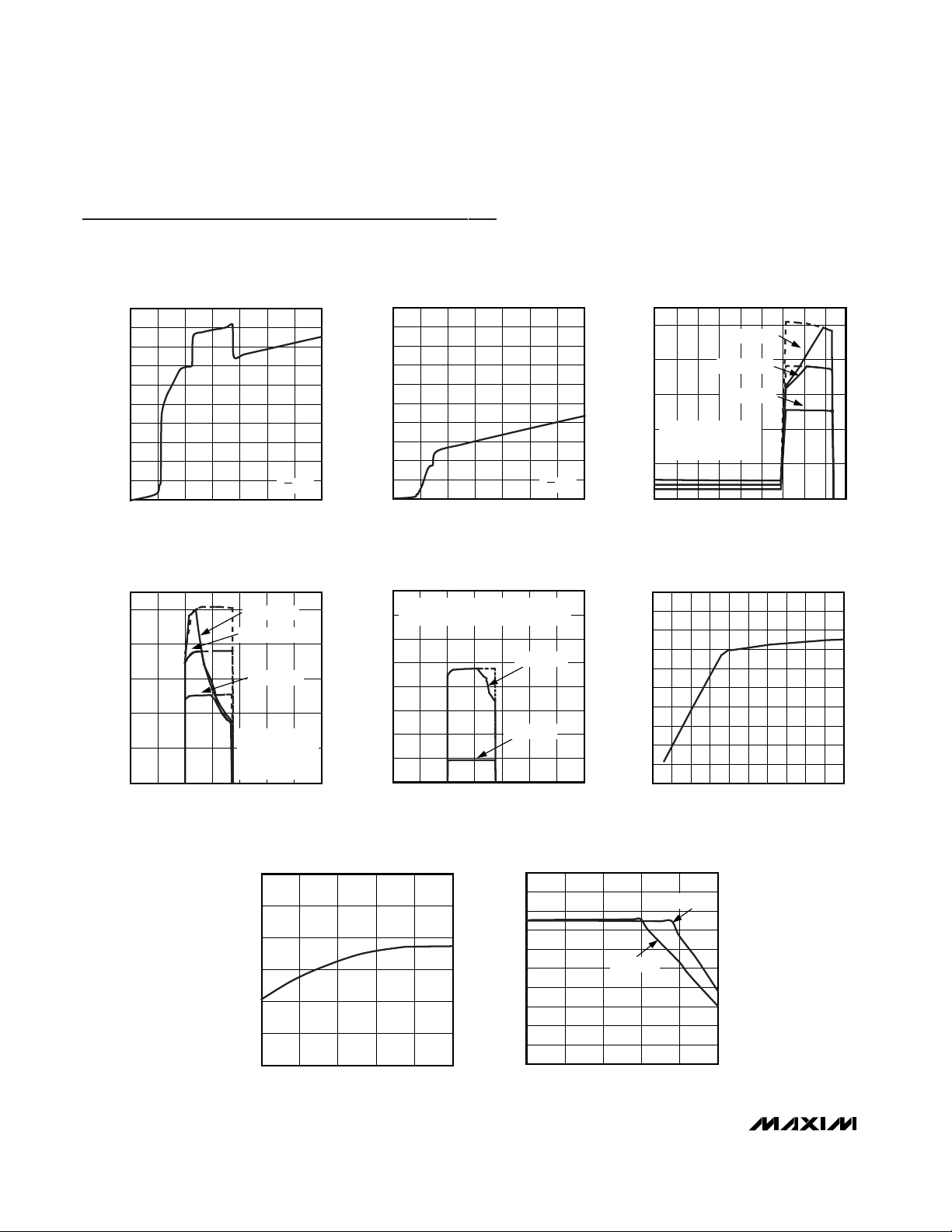
Typical Operating Characteristics
(VDC= 5V, R
SETI
= 2kΩ, V
BAT
= 3.6V, MAX8601 evaluation kit with thermal resistance of 50°C/W. TA= +25°C, unless otherwise noted.)
0
300
200
100
500
400
900
800
700
600
1000
0 2 4 6 8 10 12 14
SUPPLY CURRENT vs. INPUT VOLTAGE
MAX8600/01 toc01
INPUT VOLTAGE (V)
SUPPLY CURRENT (μA)
VEN = 0V
0
300
200
100
500
400
900
800
700
600
1000
02468101214
DISABLED SUPPLY CURRENT
vs. INPUT VOLTAGE
MAX8600/01 toc02
INPUT VOLTAGE (V)
SUPPLY CURRENT (μA)
VEN = 5V
0
200
400
600
800
1000
01.00.5 1.5 2.0 2.5 3.0 3.5 4.0 4.5
CHARGE CURRENT
vs. BATTERY VOLTAGE
MAX8600/01 toc03
V
BAT
(V)
CHARGE CURRENT (mA)
DASHED DATA TAKEN
WITH PULSE TESTING TO
AVOID THERMAL LIMIT
R
SETI
= 1.5kΩ
R
SETI
= 2kΩ
R
SETI
= 3kΩ
0
200
400
600
800
1000
02468101214
CHARGE CURRENT
vs. DC VOLTAGE
MAX8600/01 toc04
VDC (V)
CHARGE CURRENT (mA)
R
SETI
= 1.5kΩ
R
SETI
= 2kΩ
R
SETI
= 3kΩ
DASHED DATA
TAKEN WITH PULSE
TESTING TO AVOID
THERMAL LIMIT
0
200
100
400
300
700
600
500
800
04268101214
CHARGE CURRENT vs. USB VOLTAGE
MAX8600/01 toc05
V
USB
(V)
CHARGE CURRENT (mA)
V
USEL
= 0V
V
USEL
= 5V
DASHED DATA TAKEN WITH
PULSE TESTING TO AVOID THERMAL LIMIT
0
200
100
400
300
600
500
700
900
800
1000
0 0.2 0.3 0.40.1 0.5 0.6 0.7 0.90.8 1.0
CHARGE CURRENT vs. INPUT
VOLTAGE HEADROOM
MAX8600/01 toc06
(VIN - V
BAT
) (V)
CHARGE CURRENT (mA)
4.180
4.190
4.185
4.200
4.195
4.205
4.210
-40 10-15 35 60 85
BATTERY REGULATION
VOLTAGE vs. AMBIENT TEMPERATURE
MAX8600/01 toc07
TA (°C)
BATTERY REGULATION VOLTAGE (V)
0
300
200
100
400
500
600
700
800
900
1000
-40 10-15 35 60 85
CHARGE CURRENT vs. AMBIENT
TEMPERATURE (750mA CHARGE)
MAX8600/01 toc08
TA (°C)
CHARGE CURRENT (mA)
V
BAT
= 4V
V
BAT
= 3.6V
Page 5

MAX8600/MAX8601
Single-/Dual-Input 1-Cell Li+ Chargers with
OVP Protection and Programmable Charge Timer
_______________________________________________________________________________________ 5
PIN
MAX8600
NAME
FUNCTION
1 1, 7 BAT
Battery Connection. The IC delivers charging current and monitors battery voltage using BAT.
Bypass BAT to GND with a 2.2µF or larger ceramic capacitor. Connect both BAT inputs
together externally (MAX8601). BAT is high impedance when the IC is disabled.
2 2 SETI
DC Charge-Current Programming Input. Connect a resistor from SETI to GND to set the
maximum charging current when using the DC input, the prequal current from either input, and
the CHG turn-off threshold.
3 3 THM
Thermistor Input. Connect a 10kΩ NTC thermistor, in close proximity to the battery, from THM
to ground to monitor the battery temperature. Connect THM to GND to disable the thermistor
functionality. The IC suspends charging when R
THM
is outside the hot and cold limits.
4 4 GND Ground
55CT
Timing Capacitor Input. Connect a capacitor from CT to GND to set the precharge timeout,
top-off time, and fast-charge timeout. Connect CT to GND to disable the timers.
6, 7, 9 — N.C. No Connection. Make no external circuit connection.
88EN
Active-Low Enable Input. Drive low or connect EN to GND to enable the charger. Drive EN high
to disable the charger.
10 10 POK
Power-OK Monitor. POK is an open-drain output that pulls low when a valid charging source is
detected at either DC or USB (MAX8601). POK is high impedance when EN is high.
11 11 CHG
Charging-Status Output. CHG goes low when the battery is above 3V and being charged with
a current greater than 7.5% of the current programmed with R
SETI
. CHG is high impedance
when the charger is in prequal, top-off, or disabled.
Pin Description
Typical Operating Characteristics (continued)
(VDC= 5V, R
SETI
= 2kΩ, V
BAT
= 3.6V, MAX8601 evaluation kit with thermal resistance of 50°C/W. TA= +25°C, unless otherwise noted.)
100
400
300
200
500
600
700
800
900
1000
1100
-40 10-15 35 60 85
CHARGE CURRENT vs. AMBIENT
TEMPERATURE (1A CHARGE)
MAX8600/01 toc09
TA (°C)
CHARGE CURRENT (mA)
V
BAT
= 4V
V
BAT
= 3.6V
R
SETI
= 1.5kΩ
0
100
200
300
400
500
600
700
800
0.010 0.045 0.080 0.115 0.150
FAST-CHARGE TIME vs. C
CT
MAX8600/01 toc10
CCT (μF)
FAST-CHARGE TIME (MIN)
MAX8601
Page 6

MAX8600/MAX8601
Single-/Dual-Input 1-Cell Li+ Chargers with
OVP Protection and Programmable Charge Timer
6 _______________________________________________________________________________________
PIN
MAX8600
NAME
FUNCTION
12, 13 12, 13 DC
DC Input Supply. Connect DC to a 4.5V to 7V charging source. Bypass DC to GND with a 1µF
or larger capacitor. DC takes priority over USB when both are present (MAX8601). Both DC
inputs should be connected together externally.
14 14 FLT
Fault Status Output. FLT goes low when either the prequal timer or the fast-charge timers
expire and the battery voltage is not above the required threshold. Clear the fault by raising EN
or removing input power.
— 9 USB
USB Input Source. Connect to a USB port. Bypass USB to GND with a 1µF or larger capacitor.
—6
USB Charge-Select Input. Logic input that determines the maximum charge current drawn
from the USB input. I
BAT
= 95mA when USEL = low, and I
BAT
= 475mA when USEL = high.
— — EP Exposed Paddle. Connect to the GND plane for optimum thermal dissipation.
Pin Description (continued)
ANY STATE
FAULT
CHG = HIGH
FLT = LOW
V
BAT
> 3V
R
THM
> 3.97kΩ AND
R
THM
< 28.7kΩ
R
THM
> 3.97kΩ AND
R
THM
< 28.7kΩ
R
THM
< 3.97kΩ OR
R
THM
> 28.7kΩ
R
THM
< 3.97kΩ OR
R
THM
> 28.7kΩ
I
BAT
< 112.5 / R
SETI
AND VOLTAGE MODE
V
IN
< 4.1V OR
V
IN
< 7.5V OR
V
IN
< V
BAT
OR
EN HIGH
V
BAT
< 3V AND
PREQUAL
TIMEOUT
I
BAT
> 112.5 / R
SETI
AND FAST-CHARGE
TIMEOUT
TOP-OFF
TIMEOUT
OFF
POK = HIGH, CHG = HIGH, FLT = HIGH
I
BAT
= 0A
EN LOW AND
POWER-GOOD
PREQUAL
POK = LOW, CHG = HIGH
I
BAT
= 150 / R
SETI
DONE
POK = LOW, CHG = HIGH
I
BAT
= 0A
TOP-OFF
POK = LOW, CHG = HIGH
FAST-CHARGE
POK = LOW, CHG = LOW
I
BAT(DC)
= 1500 / R
ISET
I
BAT(USB)
= 100mA / 500mA
THM OUT OF RANGE
POK = PREVIOUS STATE
CHG = PREVIOUS STATE
I
BAT
= 0A
PREQUAL TIMER HELD
THM OUT OF RANGE
POK = PREVIOUS STATE
CHG = PREVIOUS STATE
I
BAT
= 0A
FAST-CHARGE TIMER HELD
Figure 1. Charger State Diagram
MAX8601
USEL
Page 7

Detailed Description
DC Charging
The MAX8600/MAX8601 are designed to charge a single-cell Li+ battery from a DC source voltage between
4.5V and 7V. The precharge current, charge current,
and top-off threshold are programmable with R
SETI
.
USB Charging (MAX8601)
The MAX8601 contains a USB input that allows operation from either a DC source or a USB port. A USEL input
allows the user to select either a 100mA or 500mA maximum charging current when using the USB input. If both
V
USB
and VDCare valid, the MAX8601 operates from
DC. If V
DC
is invalid (undervoltage/overvoltage), the
MAX8601 operates from USB. When charging at 100mA
from the USB input, the fast-charge timer is inhibited.
EN
Charger-Enable Input
EN is a logic input (active low) that enables the charger.
Drive EN high to disable the charger-control circuitry.
Drive EN low or connect to GND for normal operation.
Soft-Start
To prevent input transients, the rate of change of
charging current is limited. When the charger is turned
on or when the input source is changed, charge current
is ramped from 0 to the set current value in typically
1.2ms. This also means that if charging is taking place
from USB, and the DC input is then powered, charge
current falls to zero and then is reramped to the DC
charge rate. This is done to ensure that the DC source
is not subjected to a severe load current step.
Charge-current ramp up is also limited when transitioning from prequal to fast-charge, and when changing
the USB charge current from 100mA to 500mA with
USEL. There is no di/dt limiting, however, if I
SET
is
changed suddenly using a switch at R
SETI
.
Thermal-Limit Control
The MAX8600/MAX8601 feature a thermal limit that
reduces the charge current when the die temperature
exceeds +100°C. As the temperature increases above
+100°C, the IC lowers the charge current by 50mA/°C.
CHG
Charge-Indicator Output
CHG is an open-drain output that indicates charger status. CHG goes low during charge cycles where V
BAT
is
greater than 3V and I
BAT
is greater than 7.5% of the
maximum charge current set by R
SETI
. When the
MAX8600/MAX8601 are used in conjunction with a
microprocessor (µP), connect a pullup resistor between
CHG and the logic I/O voltage to indicate charge status
to the µP. Alternatively, CHG can sink up to 20mA for
an LED charge indicator.
Fault Indicator (
FLT
)
The MAX8600/MAX8601 contain an open-drain FLT
output to signal the user when a fault occurs. FLT goes
low if the charger is in prequal and the prequal timer
expires, or if the charger is in fast-charge and the fastcharge time expires. FLT does NOT go low if the THM
thermistor temperature is out of range. Toggle EN or
the input power to reset the FLT indicator.
Power-OK Indicator (
POK
)
The MAX8600/MAX8601 contain an open-drain POK
output that goes low when a valid input source is
detected at DC or USB (MAX8601 only). A valid input
source is one whose voltage is between 4.5V and 7V
and exceeds the battery voltage by 240mV. After a
valid input has been established, charging is sustained
with inputs as low as 3.5V as long as the input voltage
remains above the battery voltage by at least 55mV.
POK is high impedance when the charger is disabled.
Applications Information
Figure 2 shows the typical operating circuit for the
MAX8601. The following section describes component
changes for different charging current and timer durations.
MAX8600/MAX8601
Single-/Dual-Input 1-Cell Li+ Chargers with
OVP Protection and Programmable Charge Timer
_______________________________________________________________________________________ 7
BAT
NTC
10kΩ AT
+25°C
R
SETI
2kΩ
CT
THM
AC ADAPTER
4.5V TO 7V
(OVP TO 16V)
USB PORT
4.5V TO 5.5V
GND
USB
EN
OFF
ON
FLT
TO LOGIC
SUPPLY
(3.3V)
100kΩ 100kΩ 330Ω
FAULT
POWER-OK
C
CT
0.068μF
1μF
DC
SETI
USEL
POK
CHG
MAX8601
500mA
100mA
2.2μF
Figure 2. Typical Operating Circuit for USB/AC-Adapter Input
Charger. An R
SETI
of 2kΩ sets an AC adapter fast-charge of
750mA.
Page 8

MAX8600/MAX8601
Charge Current Selection
The maximum charging current from a supply connected to DC is programmed by an external resistor (R
SETI
)
connected from SETI to GND. Calculate the R
SETI
value
as follows:
R
SETI
= 1500 / I
CHARGE(MAX)
where I
CHARGE(MAX)
is in amps and R
SETI
is in ohms.
SETI can also be used to monitor the actual chargecurrent level. The output voltage at SETI is proportional
to the charging current as follows:
V
SETI
= (I
CHARGE
x R
SETI
) / 1000
Note that the prequal current for both USB and DC
input operation is 1/10 of the fast-charge current set by
R
SETI
. Also, the top-off charge-current threshold for
both USB and DC input operation is set to 7.5% of the
fast-charge current set by R
SETI
.
I
PREQUAL
= 150 / R
SETI
I
TOP-OFF
= 112.5 / R
SETI
Timer Capacitor Selection
The MAX8600/MAX8601 contain timers for prequal,
fast-charge, and top-off operation. These time periods
are determined by the capacitance from CT to GND. To
set the charge times, calculate CCTas follows:
T
FASTCHARGE
= 334min x (CCT/ 0.068µF)
T
PREQUAL
= T
TOPOFF
= 34.8min x (CCT/ 0.068µF)
Note that when charging at 100mA from the USB input
(MAX8601), the fast-charge timer is inhibited. When THM
halts charging, the timers stop and hold their value.
Battery Temperature Control
The MAX8600/MAX8601 monitor battery temperature
through a negative TC thermistor which is in close thermal contact with the battery. Select a thermistor resistance that is 10kΩ at +25°C and has a beta of 3500.
The IC compares the resistance from THM to GND and
suspends charging when it is greater than 28.3kΩ or
less than 3.94kΩ, which translates to a temperature of
0°C to +50°C. Table 1 shows the nominal temperature
limits that result from a wide range of available thermistor temperature curves. The curves are defined by the
following equation:
where β is the BETA term in Table 1.
Connect THM to GND to disable the temperature-control function. When R
THM
disables charging, all timers
pause and hold their value.
Capacitor Selection
Connect a 2.2µF ceramic capacitor from BAT to GND
for proper stability. Connect a 1µF ceramic capacitor
from DC to GND. If using the USB input for the
MAX8601, bypass USB to GND with a 1µF ceramic
capacitor. Use a larger input bypass capacitor for high
charging currents to reduce supply noise. All capacitors should be X5R dielectric or better. Be aware that
some capacitors have large voltage coefficients and
should be avoided.
Thermal Considerations
The MAX8600/MAX8601 are in a thermally enhanced
TDFN package with an exposed paddle. Connect the
exposed paddle of the package to a large copper
ground plane to provide a thermal contact between the
device and the circuit board. The exposed paddle
transfers heat away from the device, allowing the IC to
charge the battery with maximum current, while minimizing the increase in die temperature. Note that the
MAX8600/MAX8601s’ thermal-limit control allows the
charger to be tolerant of thermally restricted PC board
layouts that are sometimes unavoidable in compact
portable designs. With such non-optimal layouts, the
charger still operates, but may reduce charge current
to manage temperature rise.
RR
T
TCe
=
+
⎛
⎝
⎜
⎞
⎠
⎟
⎛
⎝
⎜
⎞
⎠
⎟
⎡
⎣
⎢
⎤
⎦
⎥
⎧
⎨
⎪
⎩
⎪
⎫
⎬
⎪
⎭
⎪
°×
−
25
1
2731298
β
Single-/Dual-Input 1-Cell Li+ Chargers with
OVP Protection and Programmable Charge Timer
8 _______________________________________________________________________________________
THERMISTOR BETA 3000 3250 3500 3750
Resistance at +25°C 10,000Ω 10,000Ω 10,000Ω 10,000Ω
Resistance at +50°C 4587.78Ω 4299.35Ω 4029.06Ω 3775.75Ω
Resistance at 0°C 25,140.55Ω 27,148.09Ω 29,315.94Ω 31,656.90Ω
Nominal Hot Trip Temperature +55.14°C +52.60°C +50.46°C +48.63°C
Nominal Cold Trip Temperature -3.24°C -1.26°C +0.46°C +1.97°C
Table 1. Fault Temperatures for Different Thermistors
Page 9
DC Input Sources
The MAX8600/MAX8601 operating input voltage range
is 4.15V to 7V. The device survives input voltages up to
16V without damage to the IC. If the input voltage is
greater than 7.5V (typ), the IC stops charging. An
appropriate power supply must provide at least 4.2V
plus the voltage drop across the internal pass transistor
when sourcing the desired maximum charging current.
V
IN(MIN)
> 4.2V + I
CHARGE(MAX)
x R
ON
where RONis the input-to-BAT resistance (typically
0.5Ω). Failure to meet this requirement results in an
incomplete charge or increased charge time.
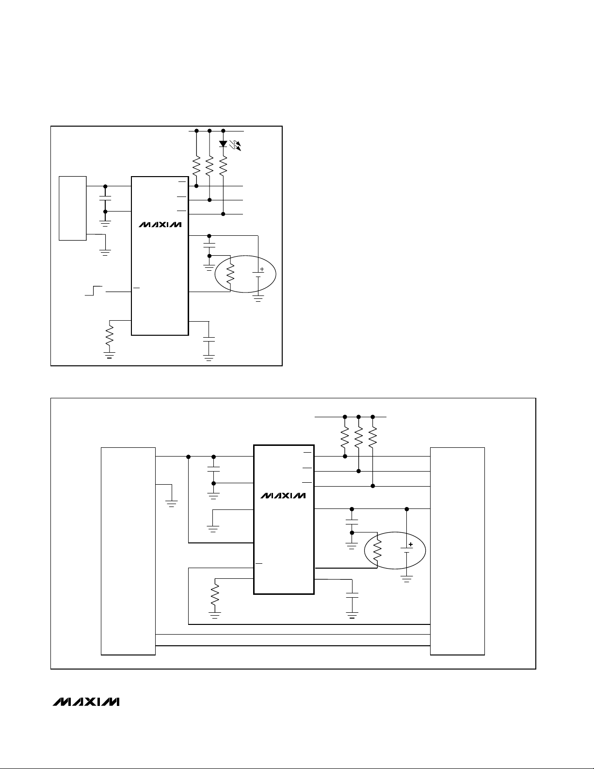
Stand-Alone Li+ Charger
The MAX8600 provides a complete Li+ charging solution. Figure 3 shows the MAX8600 as a stand-alone Li+
battery charger. The 2kΩ resistor connected to SETI
sets a charging current of 750mA. The LED indicates
when fast-charge has begun. When fast-charge is complete, the LED turns off.
USB-Powered Li+ Charger (MAX8601)
The universal serial bus (USB) provides a high-speed
serial communication port as well as power for the
MAX8600/MAX8601
Single-/Dual-Input 1-Cell Li+ Chargers with
OVP Protection and Programmable Charge Timer
_______________________________________________________________________________________ 9
BAT
Li+
CT
THM
VBUS
GND
D+
D-
500mA
USB PORT
GND
EN
FLT
V
I/O
USB
DC
USEL
SETI
POK
R5
100kΩ
C2
2.2μF
C1
1μF
C3
0.068μF
R1
2kΩ
R3, R4
100kΩ
R2
10kΩ
CHG
MAX8601
SYSTEM
Figure 4. USB Battery Charger with the MAX8601
BAT
Li+
CT
THM
AC
ADAPTER
GND
EN
FLT
+5V
CHARGE
STATUS
D1
GREEN LED
DC
SETI
POK
C1
1μF
R5
1kΩ
C3
2.2μF
C4
0.068μF
R1
2kΩ
R3, R4
100kΩ
R2
10kΩ
CHG
MAX8600
OFF
ON
Figure 3. Stand-Alone Li+ Battery-Charger with the MAX8600
Page 10

MAX8600/MAX8601
remote device. The MAX8601 can be configured to
charge its battery at the highest current possible from
the host port. Figure 4 shows the MAX8601 configured
as a USB battery charger. A USEL input sets the maximum charging current from the USB input at 100mA or
500mA.
Layout and Bypassing
Connect the input capacitors as close to the device as
possible. Provide a large copper GND plane to allow the
exposed paddle to sink heat away from the device.
Connect the battery to BAT as close to the IC as possible to provide accurate battery voltage sensing. Make
all high-current traces short and wide to minimize voltage drops. For an example layout, refer to the MAX8601
evaluation kit.
Chip Information
TRANSISTOR COUNT: 6838
PROCESS: BiCMOS
Single-/Dual-Input 1-Cell Li+ Chargers with
OVP Protection and Programmable Charge Timer
10 ______________________________________________________________________________________
TOP VIEW
8
9
10
11
12
13
14
7
6
5
4
3
2
1
MAX8601
TDFN
SETI
BAT
THM
GND
CT
USEL
BAT
FLT
DC
DC
CHG
POK
USB
EN
Pin Configurations (continued)
Page 11

MAX8600/MAX8601
Single-/Dual-Input 1-Cell Li+ Chargers with
OVP Protection and Programmable Charge Timer
______________________________________________________________________________________ 11
6, 8, &10L, DFN THIN.EPS
Package Information
(The package drawing(s) in this data sheet may not reflect the most current specifications. For the latest package outline information
go to www.maxim-ic.com/packages
.)
Page 12

MAX8600/MAX8601
Single-/Dual-Input 1-Cell Li+ Chargers with
OVP Protection and Programmable Charge Timer
12 ______________________________________________________________________________________
COMMON DIMENSIONS
SYMBOL MIN. MAX.
A 0.70 0.80
D 2.90 3.10
E 2.90 3.10
A1
0.00 0.05
L 0.20 0.40
PKG. CODE N D2 E2 e JEDEC SPEC b
[(N/2)-1] x e
PACKAGE VARIATIONS
0.25 MIN.k
A2 0.20 REF.
2.00 REF0.25±0.050.50 BSC2.30±0.1010T1033-1
2.40 REF0.20±0.05- - - - 0.40 BSC1.70±0.10 2.30±0.1014T1433-1
1.50±0.10 MO229 / WEED-3
0.40 BSC - - - - 0.20±0.05 2.40 REFT1433-2 14 2.30±0.101.70±0.10
T633-2 6 1.50±0.10 2.30±0.10 0.95 BSC MO229 / WEEA 0.40±0.05 1.90 REF
T833-2 8 1.50±0.10 2.30±0.10 0.65 BSC MO229 / WEEC 0.30±0.05 1.95 REF
T833-3 8 1.50±0.10 2.30±0.10 0.65 BSC MO229 / WEEC 0.30±0.05 1.95 REF
2.30±0.10 MO229 / WEED-3 2.00 REF0.25±0.050.50 BSC1.50±0.1010T1033-2
Package Information (continued)
(The package drawing(s) in this data sheet may not reflect the most current specifications. For the latest package outline information
go to www.maxim-ic.com/packages
.)
Page 13

MAX8600/MAX8601
Single-/Dual-Input 1-Cell Li+ Chargers with
OVP Protection and Programmable Charge Timer
Maxim cannot assume responsibility for use of any circuitry other than circuitry entirely embodied in a Maxim product. No circuit patent licenses are
implied. Maxim reserves the right to change the circuitry and specifications without notice at any time.
Maxim Integrated Products, 120 San Gabriel Drive, Sunnyvale, CA 94086 408-737-7600 ____________________ 13
© 2008 Maxim Integrated Products is a registered trademark of Maxim Integrated Products, Inc.
REVISIO N
NUMBER
REVISIO N
DATE
DESCRIPTION
PAGES
CHANGED
2 7/08 Corrected Absolute Maximum Rating 2
Revision History
 Loading...