

Page 1
General Description
The MAX8597/MAX8598/MAX8599 voltage-mode PWM
step-down controllers are designed to operate from a
4.5V to 28V input supply and generate output voltages
down to 0.6V. A proprietary switching algorithm stretches the duty cycle to >99.5% for low-dropout design.
Unlike conventional step-down regulators using a pchannel high-side MOSFET to achieve high duty cycle,
the MAX8597/MAX8598/MAX8599 drive n-channel
MOSFETs resulting in high efficiency and high-currentcapability designs.
The MAX8597 is available in a 20-pin thin QFN package and is designed for applications that use an analog
signal to control the output voltage with an adjustable
offset, such as DC fan-speed control. This is achieved
with an internal uncommitted operational amplifier. The
MAX8597 is also targeted for tracking output-voltage
applications for chipsets, ASIC and DSP cores, and I/O
supplies. The MAX8598/MAX8599 are available in a 16pin thin QFN package and do not have the uncommitted
operational amplifier, reference input, and reference output, but offer an open-drain, power-OK output.
The MAX8597/MAX8598/MAX8599 allow startup with
prebias voltage on the output for applications where a
backup supply or a tracking device may charge the
output capacitor before the MAX8597/MAX8598/
MAX8599 are enabled. In addition, the MAX8599 features output overvoltage protection.
These controllers also feature lossless high-side peak
inductor current sensing, adjustable current limit, and
hiccup-mode short-circuit protection. Switching frequency is set with an external resistor from 200kHz to
1.4MHz. This wide frequency range combined with a
wide-bandwidth error amplifier enables the loop compensation scheme to give the user ample flexibility to
optimize for cost, size, and efficiency.
Applications
Nonisolated Power Modules
Variable-Speed DC Fan Power Supplies
(MAX8597)
Tracking Power Supplies (MAX8597)
Chipset Power Supplies
Features
♦ Low Dropout with >99.5% Duty Cycle
♦ Lossless High-Side Current Limit
♦ Wide 4.5V to 28V Input Range
♦ Dynamic Output Voltage Adjustment with
Adjustable Offset (MAX8597)
♦ Remote Voltage Sensing for Both Positive and
Negative Rails (MAX8597)
♦ Tracking Output Through REFIN (MAX8597)
♦ Adjustable Switching Frequency from 200kHz to
1.4MHz
♦ Adjustable Soft-Start
♦ Prebias Startup
♦ Enable and Power-OK (MAX8598/MAX8599) for
Flexible Sequencing
♦ 25MHz Error Amplifier
♦ Adjustable Hiccup Current Limit for Output
Short-Circuit Protection
♦ Output Overvoltage Protection (MAX8599)
♦ Small, Low-Profile Thin QFN Package
MAX8597/MAX8598/MAX8599
Low-Dropout, Wide-Input-Voltage,
Step-Down Controllers
________________________________________________________________ Maxim Integrated Products 1
Ordering Information
19-3505; Rev 1; 6/05
For pricing, delivery, and ordering information, please contact Maxim/Dallas Direct! at
1-888-629-4642, or visit Maxim’s website at www.maxim-ic.com.
EVALUATION KIT
AVAILABLE
+Denotes lead-free package.
Pin Configurations appear at end of data sheet.
PART TEMP RANGE PIN-PACKAGE
MAX8597ETP -40°C to +85°C
MAX8597ETP+ -40°C to +85°C
MAX8598ETE -40°C to +85°C
MAX8598ETE+ -40°C to +85°C
MAX8599ETE -40°C to +85°C
MAX8599ETE+ -40°C to +85°C
20 Thin QFN 4mm x 4mm
(T2044-3)
20 Thin QFN 4mm x 4mm
(T2044-3)
16 Thin QFN 4mm x 4mm
(T1644-4)
16 Thin QFN 4mm x 4mm
(T1644-4)
16 Thin QFN 4mm x 4mm
(T1644-4)
16 Thin QFN 4mm x 4mm
(T1644-4)
Page 2
MAX8597/MAX8598/MAX8599
Low-Dropout, Wide-Input-Voltage,
Step-Down Controllers
2 _______________________________________________________________________________________
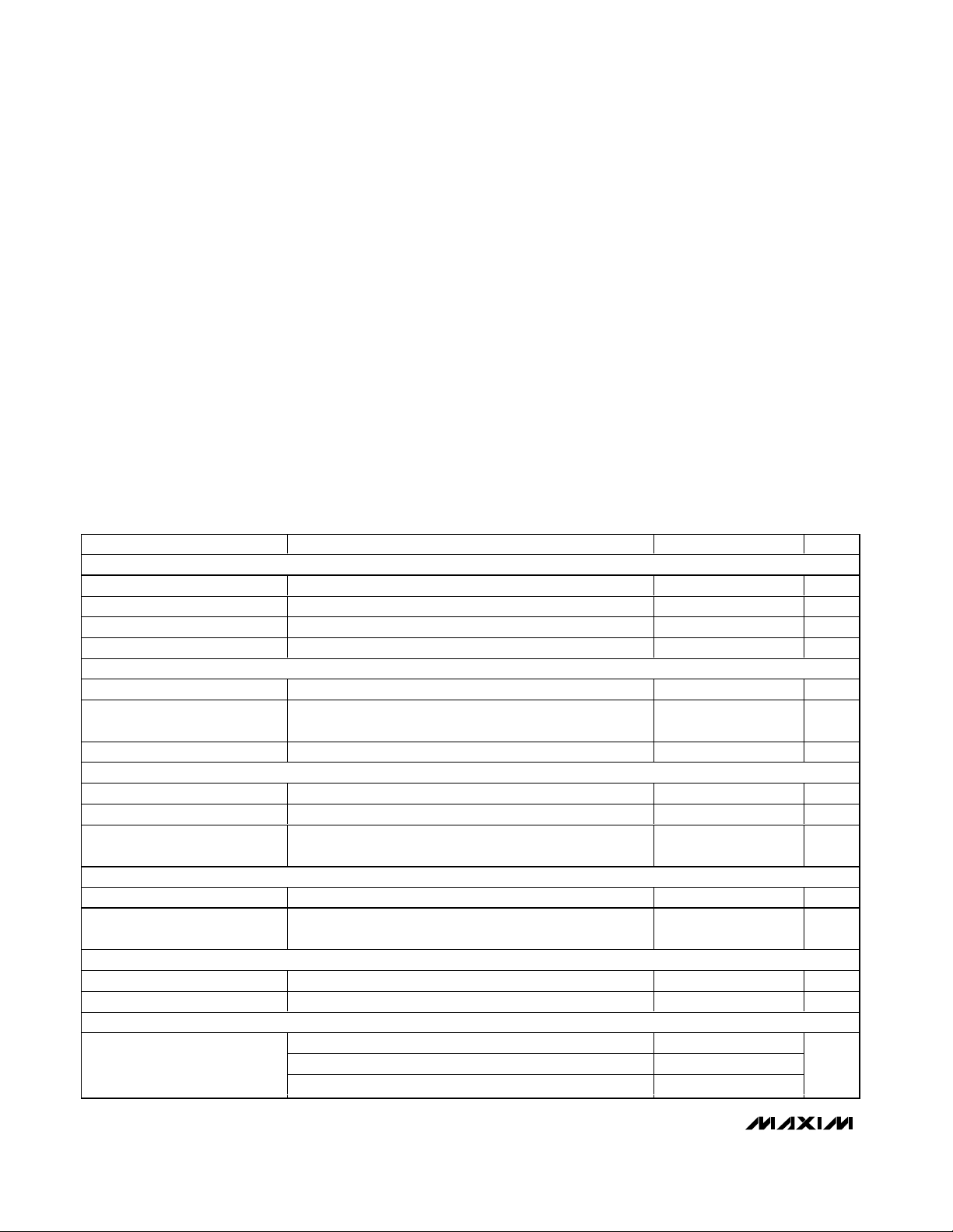
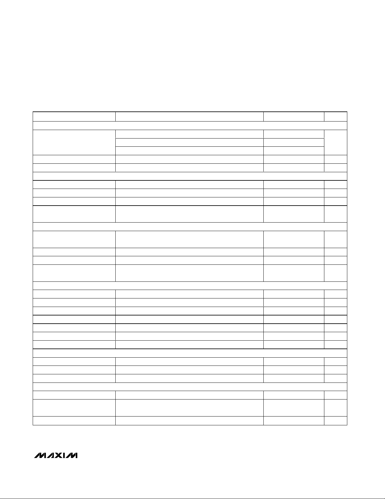
ABSOLUTE MAXIMUM RATINGS
ELECTRICAL CHARACTERISTICS
(VV+= VVL= V
AVL
= VEN= V
REFIN
= 5V, V
BST
= 6V, VLX= 1V, CVL= 4.7µF, C
REFOUT
= 1µF, V
AIN-
= V
AOUT
, V
AIN+
= 2.5V, V
ILIM
=
V
LX
- 0.2V, VFB= 0.65V, GND = PGND = 0V, CSS= 0.01µF, R
FREQ
= 20kΩ, TA= 0°C to +85°C, typical values are at TA= +25°C,
unless otherwise noted.)
Stresses beyond those listed under “Absolute Maximum Ratings” may cause permanent damage to the device. These are stress ratings only, and functional
operation of the device at these or any other conditions beyond those indicated in the operational sections of the specifications is not implied. Exposure to
absolute maximum rating conditions for extended periods may affect device reliability.
V+, ILIM to GND .....................................................-0.3V to +30V
AVL, VL to GND........................................................-0.3V to +6V
PGND to GND .......................................................-0.3V to +0.3V
FB, EN, POK, AIN-, AIN+, REFIN to GND ................-0.3V to +6V
AOUT, REFOUT, FREQ, SS, COMP to
GND .....................................................-0.3V to (V
AVL
+ 0.3V)
BST to GND ............................................................-0.3V to +36V
DH to LX....................................................-0.3V to (V
BST
+ 0.3V)
LX to GND ........................-2V (-2.5V for less than 50ns) to +30V
LX to BST..................................................................-6V to +0.3V
DL to PGND.................................................-0.3V to (V
VL
+ 0.3V)
Continuous Power Dissipation
16- or 20-Pin Thin QFN
Up to +70°C (derate 16.9mW/°C above +70°C)........1349mW
Operating Temperature Range ...........................-40°C to +85°C
Junction Temperature......................................................+150°C
Storage Temperature Range .............................-65°C to +150°C
Lead Temperature (soldering, 10s) .................................+300°C
PARAMETER CONDITIONS MIN TYP MAX UNITS
GENERAL
V+ Operating Range 5.5 28.0 V
V+/VL Operating Range V+ = VL 4.5 5.5 V
V+ Operating Supply Current V
V+ Standby Supply Current V
= 12V, VL unloaded, no MOSFETs connected, VFB = 0V 3.4 5.0 mA
V+
= 12V, VL unloaded, VFB = 0V 2.0 mA
V+
VL REGULATOR
Output Voltage 5.5V < V
VL Undervoltage-Lockout
Trip Level
Rising edge, typical hysteresis = 460mV 4.05 4.2 4.35 V
< 28V, 1mA < I
V+
Thermal Shutdown Rising temperature, typical hysteresis = 10°C +160 °C
REFERENCE (MAX8597 only)
REFOUT Output Voltage I
REFOUT Load Regulation I
REFOUT Internal Discharge
Switch On-Resistance
= 150µA, VV+ = VVL = 4.5V or 5.5V 2.49 2.50 2.51 V
REFOUT
= 10µA to 1mA 10 mV
REFOUT
During VL UVLO 15 Ω
CURRENT-LIMIT COMPARATOR (all current limits are tested at V
ILIM Sink Current 1.8V < V
Comparator Input Offset
Voltage Error
SOFT-START
Soft-Start Source Current V
Soft-Start Sink Current V
FREQUENCY
V
LX
SS
SS
R
FREQ
R
FREQ
R
FREQ
< 28V, V
LX
= 28V, V
= 100mV 3 5 7 µA
= (0.6V or V
BST
= 100kΩ 150 200 240
= 20.0kΩ 800 1000 1200Frequency
= 14.3kΩ 1100 1400 1700
= VLX + 5V 180 200 220 µA
BST
= VLX + 5V -10 +10 mV
) 3 5 7 µA
REFIN
< 35mA 4.7 5.0 5.3 V
LOAD
= VVL = 4.5V and 5.5V)
V+
kHz
Page 3
MAX8597/MAX8598/MAX8599
Low-Dropout, Wide-Input-Voltage,
Step-Down Controllers
_______________________________________________________________________________________ 3
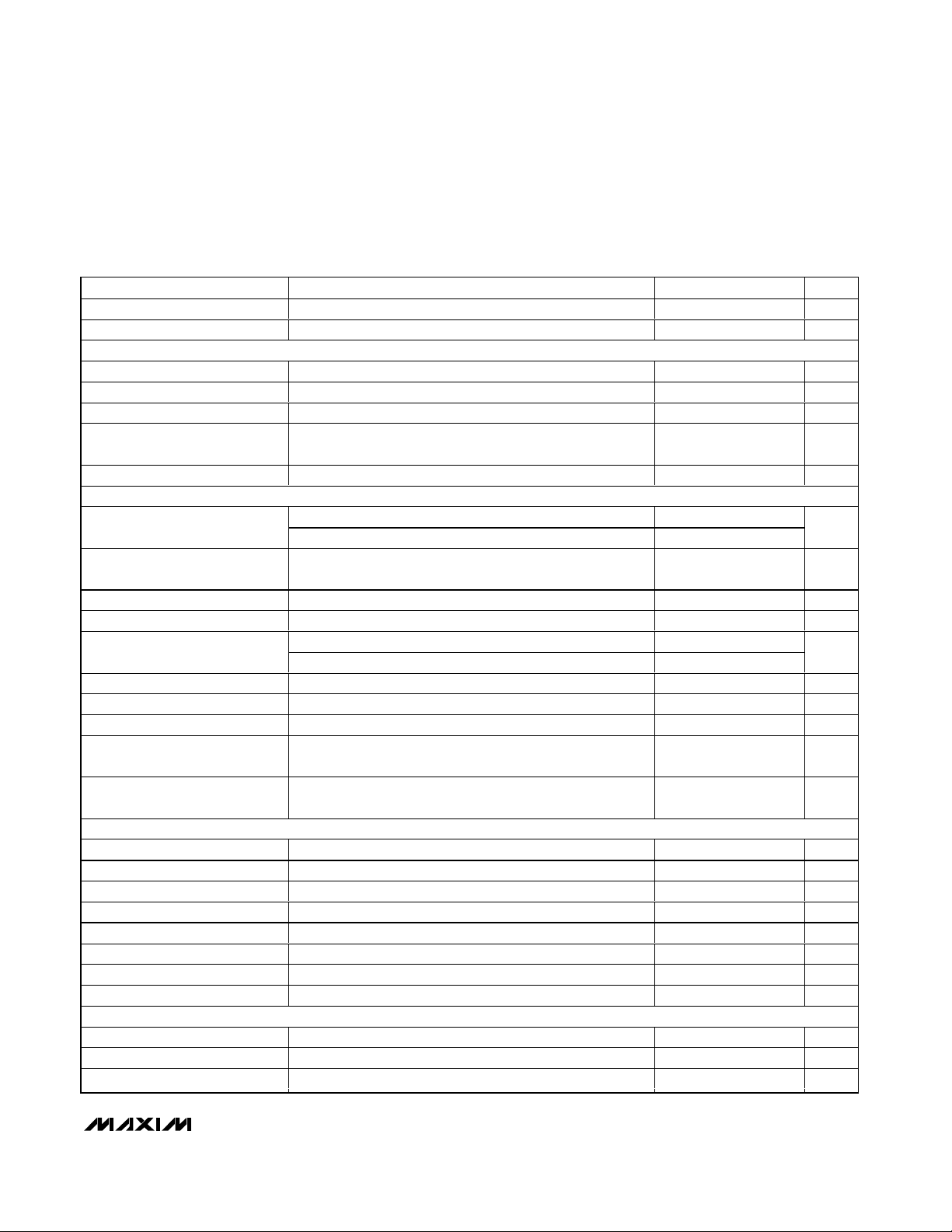
ELECTRICAL CHARACTERISTICS (continued)
(VV+= VVL= V
AVL
= VEN= V
REFIN
= 5V, V
BST
= 6V, VLX= 1V, CVL= 4.7µF, C
REFOUT
= 1µF, V
AIN-
= V
AOUT
, V
AIN+
= 2.5V, V
ILIM
=
V
LX
- 0.2V, VFB= 0.65V, GND = PGND = 0V, CSS= 0.01µF, R
FREQ
= 20kΩ, TA= 0°C to +85°C, typical values are at TA= +25°C,
unless otherwise noted.)
DH Minimum Off-Time 180 200 220 ns
DH Minimum On-Time 115 140 ns
PARAMETER CONDITIONS MIN TYP MAX UNITS
FB ERROR AMPLIFIER
FB Input Bias Current 100 nA
FB Input Voltage Set Point Over load and line 0.594 0.600 0.606 V
FB Offset Error V
Error-Amp Open-Loop Voltage
Gain
Slew Rate C
UNCOMMITTED OPERATIONAL AMPLIFIER (MAX8597 only)
Open-Loop Voltage Gain (A
Output-Voltage Swing High V
Output-Voltage Swing Low V
Unity-Gain BW 1.5 MHz
Phase Margin
Slew Rate C
Input Offset Voltage VCM = 1.25V and 2.5V -3 +3 mV
Input Leakage Current -10 +10 nA
Input Common-Mode Range
(CMVR)
Common-Mode Rejection Ratio
(CMRR)
VOL
)
= 1.25V and 2.5V, measured with respect to REFIN +10 -10 mV
REFIN
= 1.2V to 2.4V 72 90 dB
V
COMP
= 80pF 18 V/µs
LOAD
R
= 100kΩ 90
LOAD
R
= 10kΩ 70
LOAD
V
-
= 2.5V, V
AIN+
= 2.5V, V
AIN+
C
= 10pF, R
LOAD
= 100pF, R
C
LOAD
= 100pF 3.5 V/µs
LOAD
AIN
AIN
- = (V
- = (V
LOAD
LOAD
- 100mV), I
AIN+
+ 100mV), I
AIN+
= 10kΩ to 100kΩ +80
= 10kΩ to 100kΩ +40
= 100µA
SOURCE
= 100µA 20 mV
SINK
AVL
20mV
+0.50
75 dB
V
AVL
2.0
D egr ees
-
DRIVERS
DH, DL Break-Before-Make Time C
DH On-Resistance in Low State V
DH On-Resistance in High State V
DL On-Resistance in Low State V
DL On-Resistance in High State V
BST Bias Current V
LX Bias Current V
BST/LX Leakage Current V
= 2000pF 20 ns
LOAD
- VLX = 5V 1.0 2.5 Ω
BST
- VLX = 5V 1.5 3.3 Ω
BST
= VV+ = 5V 0.45 1.0 Ω
VL
= VV+ = 5V 1.3 2.5 Ω
VL
= 33V, VLX = 28V, VEN = 0V 230 520 µA
BST
= 33V, VLX = 28V, VEN = 0V -230 -520 µA
BST
= VLX = 28V, VEN = 0V 50 µA
BST
LOGIC INPUTS (EN)
Input Low Level 4.5V < V
Input High Level 4.5V < V
Input Bias Current V
VL
= VV+ = V
VL
= VV+ = V
VL
= VV+ = V
< 5.5V 1.14 0.80 V
AVL
< 5.5V 2.40 1.73 V
AVL
= 5.5V, VEN = 0 to 5.5V -1 +1 µA
AVL
dB
V
V
Page 4
MAX8597/MAX8598/MAX8599
Low-Dropout, Wide-Input-Voltage,
Step-Down Controllers
4 _______________________________________________________________________________________
ELECTRICAL CHARACTERISTICS (continued)
(VV+= VVL= V
AVL
= VEN= V
REFIN
= 5V, V
BST
= 6V, VLX= 1V, CVL= 4.7µF, C
REFOUT
= 1µF, V
AIN-
= V
AOUT
, V
AIN+
= 2.5V, V
ILIM
=
V
LX
- 0.2V, VFB= 0.65V, GND = PGND = 0V, CSS= 0.01µF, R
FREQ
= 20kΩ, TA= 0°C to +85°C, typical values are at TA= +25°C,
unless otherwise noted.)
ELECTRICAL CHARACTERISTICS
(VV+= VVL= V
AVL
= VEN= V
REFIN
= 5V, V
BST
= 6V, VLX= 1V, CVL= 4.7µF, C
REFOUT
= 1µF, V
AIN-
= V
AOUT
, V
AIN+
= 2.5V, V
ILIM
=
V
LX
- 0.2V, VFB= 0.65V, GND = PGND = 0V, CSS= 0.01µF, R
FREQ
= 20kΩ, TA= -40°C to +85°C, typical values are at TA= +25°C,
unless otherwise noted.) (Note 1)
Dual Mode is a trademark of Maxim Integrated Products, Inc.
PARAMETER CONDITIONS MIN TYP MAX UNITS
REFIN INPUT (MAX8597 only)
REFIN Input Voltage Range 0 2.75 V
REFIN Dual Mode™ Threshold
REFIN Input Bias Current V
OV AND UV FAULT COMPARATORS
Upper FB Fault Threshold (OV) Rising edge, hysteresis = 15mV (MAX8599 only) 115 117 120 %
Lower FB Fault Threshold (UV) Falling edge, hysteresis = 15mV 67 70 73 %
POWER-OK OUTPUT (POK) (MAX8598/MAX8599 only)
POK Delay For both FB rising and falling edges 8
Lower FB POK Threshold FB falling, hysteresis = 20mV 85 88 90 %
POK Output Low Level I
POK Output High Leakage V
REFIN
SINK
POK
= 1.25V or 2.5V -250 +250 nA
= 2mA 0.4 V
= 5.5V 5 µA
V
AVL
1.0
-
V
AVL
-
0.5
Clock
cycles
V
PARAMETER CONDITIONS MIN TYP MAX UNITS
GENERAL
V+ Operating Range 5.5 28.0 V
V+/VL Operating Range V+ = VL 4.5 5.5 V
V+ Operating Supply Current V
= 12V, VL unloaded, no MOSFETs connected, VFB = 0V 5.0 mA
V+
VL REGULATOR
Output Voltage 5.5V < V
VL Undervoltage-Lockout Trip
Level
REFERENCE (MAX8597 only)
REFOUT Output Voltage I
REFOUT Load Regulation I
Rising edge, typical hysteresis = 460mV 4.05 4.35 V
REFOUT
REFOUT
CURRENT-LIMIT COMPARATOR (all current limits are tested at V
ILIM Sink Current V
Comparator Input Offset Voltage
Error
SOFT-START
Soft-Start Source Current V
Soft-Start Sink Current V
ILIM
-10 +10 mV
SS
SS
< 28V, 1mA < I
V+
= 150µA, VV+ = VVL = 4.5V or 5.5V 2.47 2.51 V
= 10µA to 1mA 10 mV
= V
- 0.2V, 1.8V < VLX < 28V, V
LX
= 100mV 3 7 µA
= (0.6V or V
) 3 7 µA
REFIN
< 35mA 4.7 5.3 V
LOAD
= VVL = 4.5V and 5.5V)
V+
BST
= V
LX
+ 5V
180 220 µA
Page 5
MAX8597/MAX8598/MAX8599
Low-Dropout, Wide-Input-Voltage,
Step-Down Controllers
_______________________________________________________________________________________ 5
ELECTRICAL CHARACTERISTICS (continued)
(VV+= VVL= V
AVL
= VEN= V
REFIN
= 5V, V
BST
= 6V, VLX= 1V, CVL= 4.7µF, C
REFOUT
= 1µF, V
AIN-
= V
AOUT
, V
AIN+
= 2.5V, V
ILIM
=
V
LX
- 0.2V, VFB= 0.65V, GND = PGND = 0V, CSS= 0.01µF, R
FREQ
= 20kΩ, TA= -40°C to +85°C, typical values are at TA= +25°C,
unless otherwise noted.) (Note 1)
FREQUENCY
DH Minimum Off-Time 180 230 ns
DH Minimum On-Time 140 ns
PARAMETER CONDITIONS MIN TYP MAX UNITS
R
FREQ
R
FREQ
R
FREQ
= 100kΩ 140 240
= 20.0kΩ 800 1200Frequency
= 14.3kΩ 1100 1700
kHz
FB ERROR AMPLIFIER
FB Input Bias Current 150 nA
FB Input Voltage Set Point Over load and line 0.591 0.606 V
FB Offset Error V
Error-Amp Open-Loop Voltage
Gain
UNCOMMITTED OPERATIONAL AMPLIFIER (MAX8597 only)
Output Voltage Swing High V
Output Voltage Swing Low V
Input Offset Voltage VCM = 1.25V and 2.5V -3 +3 mV
Input Common-Mode Range
(CMVR)
= 1.25V and 2.5V, measured with respect to REFIN +20 -20 mV
REFIN
= 1.2V to 2.4V 72 dB
V
COMP
V
-
AIN+
AIN+
= 2.5V, V
= 2.5V, V
AIN
AIN
- = (V
- = (V
- 100mV), I
AIN+
+ 100mV), I
AIN+
= 100µA
SOURCE
= 100µA 20 mV
SINK
AVL
20mV
+0.50
V
AVL
2.0
-
DRIVERS
DH On-Resistance in Low State V
DH On-Resistance in High State V
DL On-Resistance in Low State V
DL On-Resistance in High State V
BST Bias Current V
LX Bias Current V
BST/LX Leakage Current V
- VLX = 5V 2.5 Ω
BST
- VLX = 5V 3.3 Ω
BST
= V
VL
VL
BST
BST
BST
= 5V 1.0 Ω
V+
= VV+ = 5V 3.5 Ω
= 33V, VLX = 28V, VEN = 0V 520 µA
= 28V, V
LX
= 28V, V
LX
= 0V -520 µA
EN
= 0V 50 µA
EN
= 33V, V
= V
LOGIC INPUTS (EN)
Input Low Level 4.5V < V
Input High Level 4.5V < V
Input Bias Current V
= VV+ = V
VL
VL
VL
= V
= V
= V
V+
V+
AVL
< 5.5V 0.8 V
AVL
= V
< 5.5V 2.4 V
AVL
= 5.5V, VEN = 0 to 5.5V -1 +1 µA
REFIN INPUT (MAX8597 only)
REFIN Input Voltage Range 0 2.75 V
V
REFIN Dual-Mode Threshold
REFIN Input Bias Current V
-
AVL
1.0
= 1.25V or 2.5V -250 +250 nA
REFIN
V
-
AVL
0.5
V
V
V
Page 6
MAX8597/MAX8598/MAX8599
Low-Dropout, Wide-Input-Voltage,
Step-Down Controllers
6 _______________________________________________________________________________________
Note 1: Limits to -40°C are guaranteed by design and characterization.
ELECTRICAL CHARACTERISTICS (continued)
(VV+= VVL= V
AVL
= VEN= V
REFIN
= 5V, V
BST
= 6V, VLX= 1V, CVL= 4.7µF, C
REFOUT
= 1µF, V
AIN-
= V
AOUT
, V
AIN+
= 2.5V, V
ILIM
=
V
LX
- 0.2V, VFB= 0.65V, GND = PGND = 0V, CSS= 0.01µF, R
FREQ
= 20kΩ, TA= -40°C to +85°C, typical values are at TA= +25°C,
unless otherwise noted.) (Note 1)
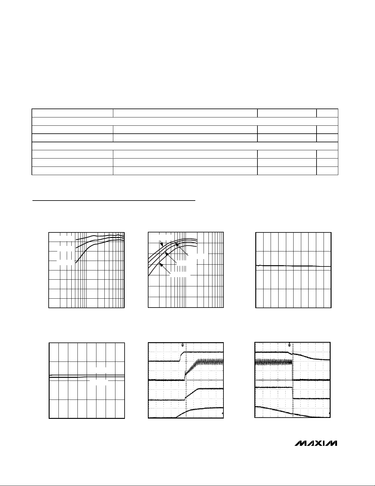
Typical Operating Characteristics
(Circuit of Figure 4, TA= +25°C, 500kHz switching frequency, VIN= 12V, unless otherwise noted.)
PARAMETER CONDITIONS MIN TYP MAX UNITS
OV AND UV FAULT COMPARATORS
Upper FB Fault Threshold (OV) Rising edge, hysteresis = 15mV (MAX8599 only) 115 120 %
Lower FB Fault Threshold (UV) Falling edge, hysteresis = 15mV 67 73 %
POWER-OK OUTPUT (POK) (MAX8598/MAX8599 only)
Lower FB POK Threshold FB falling, hysteresis = 20mV 85 90 %
POK Output Low Level I
POK Output High Leakage V
EFFICIENCY vs. LOAD CURRENT
100
V
OUT
95
V
90
85
V
80
75
EFFICIENCY (%)
70
65
60
0.1 10
CIRCUIT OF FIGURE 1
= 11.5V
= 9V
OUT
= 6V
OUT
1
LOAD CURRENT (A)
SINK
POK
= 2mA 0.4 V
= 5.5V
100
MAX8597 toc01
EFFICIENCY (%)
EFFICIENCY vs. LOAD CURRENT
CIRCUIT OF FIGURE 2
MAX8597 toc02
1.210
1.205
1.200
OUTPUT VOLTAGE (V)
1.195
1.190
020
V
= 3.3V
OUT
90
80
70
60
50
40
30
1100
V
LOAD CURRENT (A)
OUT
V
OUT
= 1.2V
= 1.8V
10
V
= 2.5V
OUT
OUTPUT VOLTAGE
vs. LOAD CURRENT
I
(A)
LOAD
5
18161412108642
µA
MAX8597 toc03
OUTPUT VOLTAGE
1.210
vs. INPUT VOLTAGE
1.205
I
LOAD
1.200
OUTPUT VOLTAGE (V)
1.195
1.190
10.0 14.0
VIN (V)
I
LOAD
= 0A
= 20A
POWER-UP WAVEFORMS
V
AVL
MAX8597 toc04
I
LX
V
OUT
V
IN
13.513.012.512.011.511.010.5
2ms/div
MAX8597 toc05
5V/div
10A/div
1V/div
10V/div
V
I
POWER-DOWN WAVEFORMS
AVL
I
LX
OUT
V
IN
MAX8597 toc06
5V/div
10A/div
1V/div
10V/div
2ms/div
Page 7
MAX8597/MAX8598/MAX8599
Low-Dropout, Wide-Input-Voltage,
Step-Down Controllers
_______________________________________________________________________________________ 7
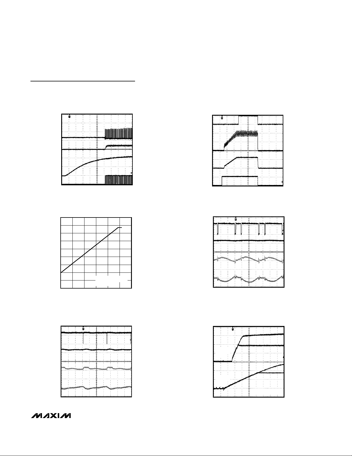
Typical Operating Characteristics (continued)
(Circuit of Figure 4, TA= +25°C, 500kHz switching frequency, VIN= 12V, unless otherwise noted.)
OUTPUT PREBIASED STARTUP
V
LX
V
OUT
V
IN
V
DL
OUTPUT VOLTAGE vs. V
1ms/div
MAX8597 toc07
10V/div
1.2V
1.0V
5V/div
5V/div
ADJ
(VIN = 12V)
13
12
11
10
9
8
7
OUTPUT VOLTAGE (V)
6
5
4
06
CIRCUIT OF FIGURE 1
= 1.2Ω
R
LOAD
V
(V)
ADJ
MAX8597 toc09
54321
V
V
OUT
V
V
V
COMP
(AC-COUPLED)
STARTUP/SHUTDOWN WITH
EN (I
POK
I
LX
EN
ENTERING DROPOUT WAVEFORMS
CIRCUIT OF FIGURE 1
V
LX
OUT
V
IN
LOAD
2ms/div
2µs/div
= 20A)
MAX8597 toc08
5V/div
10A/div
1V/div
5V/div
MAX8597 toc10
10V/div
11V
500mV/div
100mV/div
V
V
OUT
V
COMP
V
(AC-COUPLED)
HEAVY-DROPOUT WAVEFORMS
CIRCUIT OF FIGURE 1
LX
IN
10µs/div
MAX8597 toc11
10V/div
11.9V
500mV/div
500mV/div
OUTPUT TRACKING REFIN
1ms RISE
TIME
5ms RISE
TIME
1ms/div
MAX8597 toc12
CIRCUIT OF FIGURE 3
V
REFIN
V
OUT
1V/div
V
REFIN
V
OUT
1V/div
Page 8
MAX8597/MAX8598/MAX8599
Low-Dropout, Wide-Input-Voltage,
Step-Down Controllers
8 _______________________________________________________________________________________
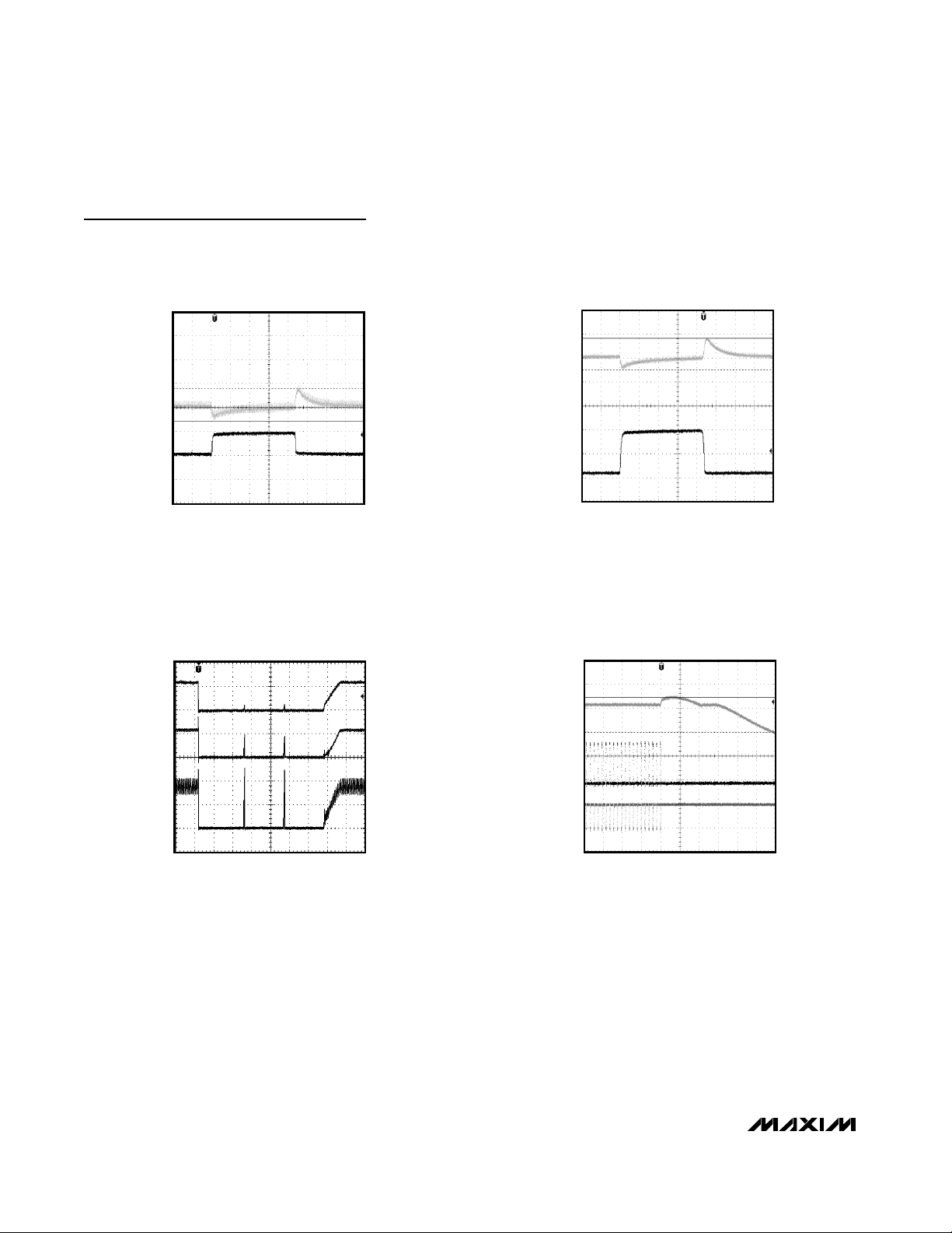
Typical Operating Characteristics (continued)
(Circuit of Figure 4, TA= +25°C, 500kHz switching frequency, VIN= 12V, unless otherwise noted.)
50% LOAD STEP AT 5A/µs
MAX8597 toc13
40µs/div
50mV/div
V
OUT
(AC-COUPLED)
I
OUT
20A
10A
90% LOAD STEP AT 5A/µs
MAX8597 toc14
40µs/div
100mV/divV
OUT
(AC-COUPLED)
I
OUT
20A
2A
SHORT-CIRCUIT RESPONSE
MAX8597 toc15
4ms/div
1V/div
2A/div
V
OUT
I
IN
I
LX
10A/div
OUTPUT OVERVOLTAGE PROTECTION
MAX8597 toc16
10µs/div
500mV/div
10V/div
V
FB
V
DH
V
DL
5V/div
Page 9

MAX8597/MAX8598/MAX8599
Low-Dropout, Wide-Input-Voltage,
Step-Down Controllers
_______________________________________________________________________________________ 9
Block Diagram
FREQ
AVL
ILIM
MAX8597
MAX8598
MAX8599
OSC
1V
P-P
PWM
BIAS
V
REG
CONTROL
LOGIC
1/20
COUNTER
REFERENCE
SOFT-START
200µA
BST
DH
LX
VL
DL
PGND
REFOUT
(MAX8597)
EN
COMP
GND
AOUT
(MAX8597)
AIN+
(MAX8597)
AIN-
(MAX8597)
(MAX8599)
OVP
EAMP
1.17 x V
REG
0.88 x V
UVP
REG
0.7 x V
REG
V+
VL
VL
SS
REFIN
(MAX8597)
FB
POK
(MAX8598/
MAX8599)
N
Page 10

MAX8597/MAX8598/MAX8599
Low-Dropout, Wide-Input-Voltage,
Step-Down Controllers
10 ______________________________________________________________________________________
Pin Description
PIN
MAX8597
MAX8598/
NAME
FUNCTION
1 1 AVL
Filtered VL Input. Connect to VL through a 10Ω resistor. Bypass to GND with a 0.22µF or larger
ceramic capacitor.
2—
External Reference Input. FB tracks the voltage input to REFIN. Connect REFIN to AVL to use
the internal 0.6V reference.
3 2 GND
Analog Ground. Connect to the exposed paddle and analog ground plane and then connect to
PGND at the output ground.
43SS
Soft-Start Programming Input. Connect a capacitor from SS to GND to set the soft-start time.
See the Selecting the Soft-Start Capacitor section for details.
54FB
Feedback Input. Connect to the center tap of an external resistor-divider to set the output
voltage. Regulates to 0.6V for the MAX8598/MAX8599 and MAX8597 when REFIN is connected
to AVL. Regulates to V
REFIN
(MAX8597) when using an external reference.
65
Compensation Input. Connect to the required compensation network. See the Compensation
Design section for details.
7 6 EN Enable Input. Drive EN high to enable the IC. Drive low to shut down the IC.
8—
Internal Reference Output. REFOUT regulates to 2.5V and can source up to 1mA. REFOUT
discharges to GND during UVLO.
97V+
Input Supply Voltage for Internal VL Regulator. Connect to an input supply in the 4.5V to 28V
range. Bypass to GND with a 1µF or larger ceramic capacitor through a 3Ω resistor.
10 8 VL
Internal 5V Linear-Regulator Output. VL provides power for the internal MOSFET gate drivers.
Bypass to PGND with a 1µF or larger ceramic capacitor. VL is always enabled except in
thermal shutdown. See the Internal 5V Linear Regulator section for details.
11 9 DL
Low-Side Gate-Driver Output. Connect to the gate of the synchronous rectifier. DL swings from
PGND to VL. DL is held low during shutdown.
12 10
Power Ground. Connect to the synchronous rectifier’s source and PGND plane.
13 11 BST
Bootstrap Input Supply for the High-Side MOSFET Driver. Connect to the cathode of an external
diode from VL and connect a 0.1µF or larger capacitor from BST to LX.
14 12 DH
High-Side Gate-Driver Output. Connect to the gate of the high-side MOSFET. DH swings from
LX to BST. DH is low (connected to LX) during shutdown.
15 13 LX
External Inductor Connection. LX is the low supply for the DH gate driver as well as the sense
connection for the current-limit circuitry. Connect LX to the switched side of the inductor as well
as the source of the high-side MOSFET and the drain of the synchronous rectifier.
16 14 ILIM
Current-Limit Sense Input. Connect a resistor from ILIM to the current-sense point to set the
output current limit. See the Setting the Current Limit section for details.
MAX8599
REFIN
COMP
REFOUT
PGND
Page 11

MAX8597/MAX8598/MAX8599
Low-Dropout, Wide-Input-Voltage,
Step-Down Controllers
______________________________________________________________________________________ 11
Pin Description (continued)
PIN
MAX8597
MAX8598/
NAME
FUNCTION
17 15
Frequency Adjust Input. Connect a resistor from FREQ to GND to set the switching frequency.
The range of the FREQ resistor is 14.3kΩ to 100kΩ (corresponding to 1400kHz to 200kHz).
18 —
Output of the Uncommitted Operational Amplifier. AOUT is high impedance during
undervoltage lockout.
19 — AIN- Inverting Input of the Uncommitted Operational Amplifier
20 — AIN+ Noninverting Input of the Uncommitted Operational Amplifier
—16POK
Power-OK Output. POK is an open-drain output that goes high impedance when the regulator
output is greater than 88% of the regulation threshold. POK is low during shutdown.
— — EP Exposed Paddle. Connect to analog ground plane for improved thermal performance.
Detailed Description
The MAX8597/MAX8598/MAX8599 voltage-mode PWM
step-down controllers are designed to operate from
4.5V to 28V input and generate output voltages down to
0.6V. A proprietary switching algorithm stretches the
duty cycle to >99.5% for low-dropout design. Unlike
conventional step-down regulators using a p-channel
high-side MOSFET to achieve high duty cycle, the
MAX8597/MAX8598/MAX8599 drive n-channel
MOSFETs permitting high efficiency and high-current
designs.
The MAX8597 is available in a 20-pin thin QFN package and is designed for applications that use an analog signal to control the output voltage with adjustable
offset, such as DC fan speed control. For example, a
12VDC fan can be driven from 6V to 12V with 12V input
power source depending on the system’s cooling
requirement to minimize fan noise and power consumption. This is achieved with an internal uncommitted
operational amplifier. With the addition of an external
RC filter, a PWM input can also be used to control the
output voltage. The MAX8597 also generates a tracking
output for chipsets, ASICs, and DSP where core and
I/O supplies are split and require tracking. In applications where tighter output tolerance is required, the
MAX8597 output can be set by an external precision
reference source feeding to REFIN. The MAX8598/
MAX8599 are available in a 16-pin thin QFN package
and do not have the uncommitted operational amplifier,
reference input, and reference output, but offer a powerOK output (POK). With the enable input and POK output, the MAX8598/MAX8599 can easily be configured to
have power sequencing of multiple supply rails.
The MAX8597/MAX8598/MAX8599 allow startup with
prebias voltage on the output for applications where a
backup supply or a tracking device may charge the
output capacitor before the MAX8597/MAX8598/
MAX8599 are enabled. The MAX8599 has output overvoltage protection.
These controllers feature lossless high-side peak
inductor current sensing, adjustable current limit, and
hiccup-mode short-circuit protection. Switching frequency is set with an external resistor from 200kHz to
1.4MHz. This wide frequency range combined with a
wide-bandwidth error amplifier enable the loop-compensation scheme to give the user ample flexibility to
optimize for cost, size, and efficiency.
DC-DC Controller
The MAX8597/MAX8598/MAX8599 step-down DC-DC
controllers use a PWM voltage-mode control scheme. An
internal high-bandwidth (25MHz) operational amplifier is
used as an error amplifier to regulate the output voltage.
The output voltage is sensed and compared with an internal 0.6V reference or REFIN (MAX8597) to generate an
error signal. The error signal is then compared with a
fixed-frequency ramp by a PWM comparator to give the
appropriate duty cycle to maintain output voltage regulation. The high-side MOSFET turns on at the rising edge of
the internal clock 20ns after DL (the low-side MOSFET
gate drive) goes low. The high-side MOSFET turns off
once the internal ramp voltage reaches the error-amplifier
output voltage. The process repeats for every clock
cycle. During the high-side MOSFET on-time, current
flows from the input through the inductor to the output
capacitor and load. At the moment the high-side MOSFET turns off, the energy stored in the inductor during the
on-time is released to support the load as the inductor
MAX8599
FREQ
AOUT
Page 12

MAX8597/MAX8598/MAX8599
current ramps down through the low-side MOSFET body
diode; 20ns after DH goes low, the low-side MOSFET
turns on, resulting in a lower voltage drop to increase efficiency. The low-side MOSFET turns off at the rising edge
of the next clock pulse, and when its gate voltage discharges to zero, the high-side MOSFET turns on and
another cycle starts.
These controllers also sense peak inductor current and
provide hiccup-overload and short-circuit protection
(see the Current Limit section). The MAX8597/
MAX8598/MAX8599 operate in forced-PWM mode
where the inductor current is always continuous. The
controller maintains constant switching frequency
under all loads, except under dropout conditions where
it skips DL pulses.
Current Limit
The MAX8597/MAX8598/MAX8599 DC-DC step-down
controllers sense the peak inductor current either with
the on-resistance of the high-side MOSFET for lossless
sensing, or a series resistor for more accurate sensing.
When the voltage across the sensing element exceeds
the current-limit threshold set with ILIM, the controller
immediately turns off the high-side MOSFET. The lowside MOSFET is then turned on to let the inductor current ramp down. As the output load current increases
above the ILIM threshold, the output voltage sags
because the truncated duty cycle is insufficient to support the load current. When FB falls 30% below its nominal threshold, the output undervoltage protection is
triggered and the controller enters hiccup mode to limit
power dissipation. This current-limit method allows the
circuit to withstand a continuous output short circuit.
The MAX8597/MAX8598/MAX8599 current-limit threshold is set by an external resistor that works in conjunction with an internal 200µA current sink (see the Setting
the Current Limit section for more details).
Synchronous-Rectifier Driver (DL)
Synchronous rectification reduces the conduction loss
in the rectifier by replacing the normal Schottky catch
diode with a low-resistance MOSFET switch. The
MAX8597/MAX8598/MAX8599 also use the synchronous rectifier to ensure proper startup of the boost
gate-drive circuit.
High-Side Gate-Drive Supply (BST)
Gate-drive voltage for the high-side n-channel MOSFET is
generated by an external flying capacitor and diode boost
circuit (D1 and C5 in Figure 1). When the synchronous
rectifier is on, C5 is charged from the VL supply through
the Schottky diode. When the synchronous rectifier is
turned off, the Schottky is reverse biased and the voltage
on C5 is stacked above LX to provide the necessary turnon voltage for the high-side MOSFET. A low-current
Schottky diode, such as Central Semiconductor’s
CMDSH-3, works well for most applications. The capacitor
should be large enough to prevent it from charging to
excessive voltage, but small enough to adequately charge
during the minimum low-side MOSFET on-time, which
occurs at minimum input voltage. A capacitor in the 0.1µF
to 0.47µF range works well for most applications.
Internal 5V Linear Regulator
The MAX8597/MAX8598/MAX8599 contain a lowdropout 5V regulator that provides up to 35mA to supply gate drive for the external MOSFETs, and supplies
AVL, which powers the IC’s internal circuitry. Bypass
the regulator’s output (VL) with 1µF per 10mA of VL
load, or greater ceramic capacitor. The current
required to drive the external MOSFET can be estimated by multiplying the total gate charge (at VGS= 5V) of
the MOSFETs by the switching frequency.
Undervoltage Lockout (UVLO)
When VVLdrops below 3.75V (typ), the MAX8597/
MAX8598/MAX8599s’ undervoltage-lockout (UVLO) circuitry inhibits switching, forces POK (MAX8598/
MAX8599) low, and forces DH and DL low. Once V
VL
rises above 4.2V (typ), the controller powers up the output in startup mode (see the Startup section).
Startup
The MAX8597/MAX8598/MAX8599 start switching once
all the following conditions are met:
1) EN is high.
2) VVL> 4.2V (typ).
3) Soft-start voltage VSSexceeds VFB.
4) Thermal limit is not exceeded.
The third condition ensures that the MAX8597/
MAX8598/MAX8599 do not discharge a prebiased output. Once all of these conditions are met, the IC begins
switching and the soft-start cycle is initiated.
Low-Dropout, Wide-Input-Voltage,
Step-Down Controllers
12 ______________________________________________________________________________________
Page 13

Power-OK Signal
(POK, MAX8598/MAX8599 Only)
The power-OK signal (POK) is an open-drain output that
goes high impedance when FB is above 91% of its nominal threshold. There is an eight clock-cycle delay before
POK goes high impedance. For 500kHz switching frequency, this delay is typically 16µs. To obtain a logic
voltage output, connect a pullup resistor from POK to
AVL. A 100kΩ resistor works well for most applications.
If unused, connect POK to GND or leave it unconnected.
Enable and Soft-Start
The MAX8597/MAX8598/MAX8599 are enabled using
the EN input. A logic high on EN enables the output of
the IC. Conversely, a logic low on EN disables the output. On the rising edge of EN, the controllers enter softstart. Soft-start gradually ramps up the reference
voltage seen at the error amplifier to control the output
rate of rise and reduce the inrush current during startup. The soft-start period is determined by a capacitor
connected from SS to GND (C6 in Figure 1). A 5µA current source charges the external capacitor to the reference voltage (0.6V or V
REFIN
). The capacitor value is
determined as follows:
where tSSis the soft-start time in seconds and VFBis
0.6V or V
REFIN
. The output reaches regulation when
soft-start is completed.
Output Undervoltage Protection (UVP)
Output UVP begins when the controller is at its current
limit and VFBis 30% below its nominal threshold. This
condition causes the controller to drive DH and DL low
and discharges the soft-start capacitor with a 5µA pulldown current until VSSreaches 50mV. Then the controller begins in soft-start mode. If the overload
condition still exists, the UVP process begins again. The
result is “hiccup” mode, where the controller attempts to
restart periodically as long as the overload condition
exists. In hiccup mode, the soft-start capacitor voltage
ramps up to 112% of the nominal V
FB
threshold and
then ramps down to 50mV. For the MAX8597, V
REFIN
must be greater than 450mV to trigger UVP. The softstart capacitor voltage then ramps up to 112% of V
REFIN
and then down to 50mV.
Output Overvoltage Protection
(OVP, MAX8599)
The output voltage is continuously monitored for overvoltage (MAX8599 only). If the output voltage is more
than 117% of its nominal set value, OVP is triggered
after a 12µs (typ) delay. The MAX8599 latches DH low
to turn off the high-side MOSFET, and DL high to turn
on the low-side MOSFET to clamp the output to PGND.
The latch is reset either by toggling EN or by cycling V+
below the UVLO threshold. Note that DL latching high
causes a negative spike at the output due to the energy
stored in the output LC at the instant of OVP trip. If the
load cannot tolerate this negative spike, add a power
Schottky diode across the output to act as a reverse
polarity clamp.
Thermal-Overload Protection
Thermal-overload protection limits the total power dissipation in the MAX8597/MAX8598/MAX8599. When the
junction temperature exceeds +160°C, a thermal sensor shuts down the device, forcing DH and DL low,
allowing the IC to cool. The thermal sensor turns the
part on after the junction temperature cools by 10°C,
resulting in a pulsed output during continuous thermaloverload conditions. During a thermal event, the switching converter is turned off, the reference is turned off,
the VL regulator is turned off, POK is high impedance,
and the soft-start capacitor is discharged.
MAX8597/MAX8598/MAX8599
Low-Dropout, Wide-Input-Voltage,
Step-Down Controllers
______________________________________________________________________________________ 13
C
65
At
=×µ
SS
V
FB
Page 14

MAX8597/MAX8598/MAX8599
Low-Dropout, Wide-Input-Voltage,
Step-Down Controllers
14 ______________________________________________________________________________________
Figure 1. MAX8597 (600kHz): Live Adjustable Output Voltage from 6V to 12V at 10A
Figure 2. 1.2V at 20A Output with Remote Sensing
Design Procedure
V
(10.8V TO 13.2V)
IN
R15
OFF
V
ADJ
(0V TO 5V)
0.01µF
R10
93.1kΩ
C15
R6
48.7kΩ
R7
48.7kΩ
ON
5.1kΩ
100pF
C10
R1
EN
AVL
R4
100kΩ
R5
32.4kΩ
6.04kΩ
R11
C6
0.033µF
47kΩ
R8
24.9kΩ
C8
4.7pF
R12
C9
820pF
R9
33.2kΩ
2 7 17 9 16
REFIN EN FREQ V+ ILIM
19
AIN-
20
AIN+
4
SS
18
AOUT
5
GNDCOMP
3
6
C11
0.22µF
C1
3Ω
1µF
MAX8597
PGND
REFOFBVL
AVL
1810
R13
10Ω
C13
1µF
BST
VL
D1
CMDSH-3
13
14
DH
15
LX
11
DL
12
C12
4.7µF
VL
1.21kΩ
IRF7821
C5
0.22µF
IRF7821
R2
Q1
Q2
C2A
10µF
C2B
10µF
C3
0.01µF
6V TO 12V/10A
C7B
47µF
V
OUT
R14
2Ω
C14
2200pF
1µH
L1
C7A
47µF
(10.8V TO 13.2V)
V
OFF
R3
10kΩ
10kΩ
IN
ON
R6
R7
12.1kΩ
7.2kΩ
1800pF
R4
10kΩ
C8
R14
C1
3Ω
R1
EN
AVL
R5
10kΩ
C4
0.033µF
R9
12.1kΩ
16kΩ
C8
39pF
R10
C9
6800pF
R8
40.2kΩ
2 7 17 9 16
REFIN EN FREQ V+ ILIM
19
AIN-
20
AIN+
4
SS
18
AOUT
5
GNDCOMP
3
6
0.22µF
1µF
MAX8597
REFOFBVL
AVL
1810
R11
10Ω
C10
C11
1µF
CMDSH-3
BST
DH
LX
DL
PGND
D1
13
14
15
11
12
C12
4.7µF
VL
VL
1.65kΩ
C5
0.22µF
R2
(Q1 = Q2 =
(Q3 = Q4 =
IRF7807Z)
IRF7832)
C3
0.01µF
C2A
10µF
C2B
10µF
C2C
10µF
Q2Q1
V
C7B
470µF
OUT
1.2V/20A
L1
0.7µH
R12
3Ω
C13
2200pF
C7A
470µF
Q4Q3
Page 15

MAX8597/MAX8598/MAX8599
Low-Dropout, Wide-Input-Voltage,
Step-Down Controllers
______________________________________________________________________________________ 15
Figure 3. MAX8597 1MHz Tracking Supply with Clamp (Output voltage tracks V
REFIN
from 0V up to the nominal output regulation
voltage.)
Figure 4. MAX8598/MAX8599 500kHz, 1.2V, 20A Output Power Supply
Design Procedure (continued)
(10.8V TO 13.2V)
V
IN
R1
20kΩ
R12
C1
3Ω
MAX8597
AVL
GNDCOMP
1810
3
10Ω
C11
0.22µF
1µF
R9
REFOFBVL
C12
1µF
BST
PGND
D1
CMDSH-3
13
14
DH
15
LX
11
DL
12
C13
4.7µF
VL
OFF
10kΩ
EN
ON
REFIN
D2
56pF
C9
8200pF
2200pF
C8
C4
1000pF
2717 9 16
REFIN EN FREQ V+ ILIM
19
AIN-
20
AIN+
C6
4
SS
18
AOUT
5
6
R3
70kΩ
CMPD914
R4
18.2kΩ
R5
6.98kΩ
R6
R7
390Ω
1000pF
C10
5.6kΩ
R8
(10.8V TO 13.2V)
V
IN
C2A
C3
0.01µF
C2A
10µF
R10
2Ω
C14
2200pF
L1
0.56µH
100µF
10µF
C2B
10µF
C7A
C7B
100µF
V
OUT
1.8V/10A
VL
R2
1.5kΩ
Q1
IRF7807Z
C5
0.22µF
Q2
IRF7821
R11
C1
3Ω
OFF
POK
1800pF
R5
12.1kΩ
1.2kΩ
C8
R1
EN
ON
R6
R4
12.1kΩ
16kΩ
100kΩ
R7
R3
C4
0.033µF
AVL
C8
39pF
C9
6800pF
40.2kΩ
6157 14
EN FREQ V+ ILIM
16
POK
3
SS
4
FB
5
COMP
GND
2
AVL
C10
0.22µF
1µF
11
BST
12
DH
C11
4.7µF
PGND
13
LX
9
DL
MAX8598
MAX8599
AVL
VL
110
8
R8
10Ω
VL
CMDSH-3
C3
0.01µF
C2B
10µF
C2C
10µF
Q1
HAT2168H
Q3
HAT2165H
R9
3Ω
C12
2200pF
0.7µH
L1
470µF
C7A
C7B
470µF
V
OUT
1.2V/20A
VL
D1
R2
2.26kΩ
C5
0.22µF
Q2
HAT2165H
Page 16

MAX8597/MAX8598/MAX8599
Low-Dropout, Wide-Input-Voltage,
Step-Down Controllers
16 ______________________________________________________________________________________
Setting the Output Voltage
Fixed Output Voltage
The output voltage is set by a resistor-divider network
from the output to GND with FB at the center tap (R4
and R5 in Figure 4). Select R4 between 5kΩ and 15kΩ
and calculate R5 by:
R5 = R4 x [( V
OUT
/ VFB) - 1]
Live Adjustable Output Voltage (see Figure 1)
Using the uncommitted operational amplifier, the
MAX8597 can be configured such that the output voltage is adjustable using a voltage source (V
ADJ
). The
following parameters must be defined before starting
the design:
• The minimum desired output voltage, V
OUT_MIN
• The maximum desired output voltage, V
OUT_MAX
• The desired input that corresponds to the minimum
output voltage, V
ADJ_MIN
• The desired input that corresponds to the maximum
output voltage, V
ADJ_MAX
Select V
AOUT
(uncommitted operational-amplifier out-
put) between 0.05V and 3V and V
AOUT_MAX
higher
than V
AOUT_MIN
. Calculate the required AIN+ reference
(V
AIN+
) as:
V
AIN+
is set using a resistor-divider from REFOUT to
GND (R6 and R7). Select R7 to be approximately 50kΩ
as a starting point and then calculate R6 as:
R6 = R7 x [(2.5V / V
AIN+
) - 1]
Select R4 to be 100kΩ and calculate R5 as:
Select R9 between 5kΩ and 15kΩ, then calculate R8
and R10 as follows:
where VFBis the feedback regulation voltage (0.6V with
REFIN connected to AVL).
Additionally, to minimize error, R6 and R7 should be
chosen such that:
Inductor Selection
There are several parameters that must be examined
when determining which inductor is to be used: input
voltage, output voltage, load current, switching frequency, and LIR. LIR is the ratio of inductor current ripple to DC load current. A higher LIR value allows for a
smaller inductor but results in higher losses and higher
output ripple. A good compromise between size and
efficiency is a 30% LIR. Once all the parameters are
chosen, the inductor value is determined as follows:
where fS is the switching frequency. Choose a standard
value close to the calculated value. The exact inductor
value is not critical and can be adjusted in order to
make trade-offs among size, cost, and efficiency.
Lower inductor values minimize size and cost, but also
increase the output ripple and reduce the efficiency
due to higher peak currents. On the other hand, higher
inductor values increase efficiency, but eventually
resistive losses due to extra turns of wire exceed the
benefit gained from lower AC current levels. Find a lowloss inductor having the lowest possible DC resistance
that fits the allotted dimensions. Ferrite cores are often
the best choice, although powdered iron is inexpensive
and can work well up to 300kHz. The chosen inductor’s
saturation current rating must exceed the peak inductor
current determined as:
Input Capacitor
The input filter capacitor reduces peak currents drawn
from the power source and reduces noise and voltage
ripple on the input caused by the circuit’s switching.
The input capacitor must meet the ripple current
requirement (I
RMS
) imposed by the switching currents
defined by the following equation:
V
AIN
VVVV
AOUT MAX ADJ MAX AOUT MIN ADJ MIN
=
+
()( )
VV V V
ADJ MAX ADJ MIN AOUT MAX AOUT MIN
××
__ __
−−
__ _ _
−
+
R
VV R
( )
54
AIN AOUT MIN
=
−
+
VV
( )
ADJ MAX AIN
_
_
−
×
+
RR
67
×
RR
67
+
RR
45
×
=
RR
45
+
VxVV
L
=
II
PEAK LOAD MAX LOAD MAX
OUT IN OUT
V x f x I x LIR
IN S LOAD MAX
=+
() ()
−
()
()
LIR
⎛
⎞
I
⎜
⎝
×
⎟
⎠
2
VVVV V VV V
()
OUT MIN FB FB AOUT MIN OUT MAX FB AOUT MAX FB
[ ]
R
8 9
=
×
−− − −
____
()
VVVVV
()()
()
OUT MAX FB OUT MIN FB FB
__
+
()
−− −
×
()
×
R
×
RR V V
89
××
R
10
=
VR VV R
89
×
+
()
()
FB FB AOUT MIN
[]
−
()
OUT MAX FB
_
−
×
_
I
RMS
IVVV
=
××
LOAD OUT IN OUT
()
V
IN
−
Page 17

MAX8597/MAX8598/MAX8599
Low-Dropout, Wide-Input-Voltage,
Step-Down Controllers
______________________________________________________________________________________ 17
I
RMS
has a maximum value when the input voltage
equals twice the output voltage (VIN= 2 x V
OUT
), so
I
RMS(MAX)
= I
LOAD
/ 2. Ceramic capacitors are recommended due to their low ESR and ESL at high frequency, with relatively lower cost. Choose a capacitor that
exhibits less than 10°C temperature rise at the maximum
operating RMS current for optimum long-term reliability.
Output Capacitor
The key selection parameters for the output capacitor
are the actual capacitance value, the equivalent series
resistance (ESR), the equivalent series inductance
(ESL), and the voltage-rating requirements, which
affect the overall stability, output ripple voltage, and
transient response. The output ripple has three components: variations in the charge stored in the output
capacitor, voltage drop across the capacitor’s ESR,
and voltage drop across the capacitor’s ESL, caused
by the current into and out of the capacitor. The following equations estimate the worst-case ripple:
where I
P-P
is the peak-to-peak inductor current.
The response to a load transient depends on the selected output capacitor. After a load transient, the output
instantly changes by (ESR x ∆I
LOAD
) + (ESL x di/dt).
Before the controller can respond, the output deviates
further depending on the inductor and output capacitor
values. After a short period of time (see the Typical
Operating Characteristics), the controller responds by
regulating the output voltage back to its nominal state.
The controller response time depends on the closedloop bandwidth. With higher bandwidth, the response
time is faster, preventing the output capacitor voltage
from further deviation from its regulation value. Do not
exceed the capacitor’s voltage or ripple current ratings.
MOSFET Selection
The MAX8597/MAX8598/MAX8599 controllers drive
external, logic-level, n-channel MOSFETs as the circuitswitch elements. The key selection parameters are:
• On-resistance (R
DS(ON)
): the lower, the better.
• Maximum drain-to-source voltage (V
DSS
): should be
at least 20% higher than the input supply rail at the
high-side MOSFET’s drain.
• Gate charges (Qg, Qgd, Qgs): the lower, the better.
Choose MOSFETs with R
DS(ON)
rated at VGS= 4.5V. For
a good compromise between efficiency and cost,
choose the high-side MOSFET that has conduction loss
equal to the switching loss at the nominal input voltage
and maximum output current. For the low-side MOSFET,
make sure it does not spuriously turn on due to dv/dt
caused by the high-side MOSFET turning on, resulting in
efficiency degrading shoot-through current. MOSFETs
with a lower Q
gd/Qgs
ratio have higher immunity to dv/dt.
For proper thermal-management design, the power dissipation must be calculated at the desired maximum
operating junction temperature, maximum output current,
and worst-case input voltage (for low-side MOSFET,
worst case is at V
IN(MAX)
; for high-side MOSFET, it could
be either at V
IN(MIN)
or V
IN(MAX)
).
High-side and low-side MOSFETs have different loss
components due to the circuit operation. The low-side
MOSFET operates as a zero-voltage switch; therefore,
the major losses are the channel-conduction loss
(P
LSCC
) and the body-diode conduction loss (P
LSDC
):
P
LSCC
= [1 - (V
OUT
/ VIN)] x (I
LOAD
)2x R
DS(ON)
P
LSDC
= 2 x I
LOAD
x VFx tdtx f
S
where VFis the body-diode forward-voltage drop, tdtis
the dead-time between the high-side MOSFET and the
low-side MOSFET switching transitions, and fSis the
switching frequency. The high-side MOSFET operates
as a duty-cycle control switch and has the following
major losses: the channel-conduction loss (P
HSCC
), the
V-I overlapping switching loss (P
HSSW
), and the drive
loss (P
HSDR
). The high-side MOSFET does not have
body-diode conduction loss because the diode never
conducts current:
P
HSCC
= (V
OUT
/ VIN) x I
LOAD
2
x R
DS(ON)
Use R
DS(ON)
at T
J(MAX)
:
P
HSSW
= VINx I
LOAD
x fSx [(Qgs+ Qgd) / I
GATE
]
where I
GATE
is the average DH-high driver output-cur-
rent capability determined by:
I
GATE
= 2.5 / (RDH+ R
GATE
)
VV V V
V I ESR
V
V
I
PP
=++
RIPPLE RIPPLE ESR RIPPLE ESL RIPPLE C
RIPPLE ESR P P
RIPPLE ESL
RIPPLE C
−
()
()
=
()
⎛
VV
IN OUT
=
⎜
fLVV
⎝
S
() () ()
=×
−
V ESL
×
IN
=
L ESL
+
I
PP
8
−
×
−
××
Cf
OUT S
⎞
⎟
⎠
⎛
×
⎜
⎝
OUT
IN
⎞
⎟
⎠
Page 18

MAX8597/MAX8598/MAX8599
where RDHis the high-side MOSFET driver’s average
on-resistance (1.25Ω typ) and R
GATE
is the internal
gate resistance of the MOSFET (typically 0.5Ω to 2Ω):
P
HSDR
= Qgsx VGSx fSx R
GATE
/ (R
GATE
+ RDH)
where VGS~ VVL= 5V.
In addition to the losses above, add approximately
20% more for additional losses due to MOSFET output
capacitances and low-side MOSFET body-diode
reverse-recovery charge dissipated in the high-side
MOSFET that exists, but is not well defined in the
MOSFET data sheet. Refer to the MOSFET data sheet
for thermal-resistance specification to calculate the
PC board area needed to maintain the desired maximum operating junction temperature with the abovecalculated power dissipation. To reduce EMI caused
by switching noise, add a 0.1µF or larger ceramic
capacitor from the high-side switch drain to the lowside switch source or add resistors in series with DH
and DL to slow down the switching transitions.
However, adding a series resistor increases the power
dissipation of the MOSFETs, so be sure this does not
overheat the MOSFETs. The minimum load current must
exceed the high-side MOSFET’s maximum leakage plus
the maximum LX bias current over temperature.
Setting the Current-Limit
The MAX8597/MAX8598/MAX8599 controllers sense
the peak inductor current to provide constant-current
and hiccup current limit. The peak current-limit threshold is set by an external resistor (R2 in Figure 1) together with the internal current sink of 200µA. The voltage
drop across the resistor R2 due to the 200µA current
sets the maximum peak inductor current that can flow
through the high-side MOSFET or the optional currentsense resistor (between the high-side MOSFET source
and LX) by the equations below:
I
PEAK(MAX)
= 200µA x R2 / R
DSON(HSFET)
I
PEAK(MAX)
= 200µA x R2 / R
SENSE
The actual corresponding maximum load current is
lower than the I
PEAK(MAX)
by half of the inductor ripple
current. If the R
DS(ON)
of the high-side MOSFET is used
for current sensing, use the maximum R
DS(ON)
at the
highest operating junction temperature to avoid false
tripping of the current limit at elevated temperature.
Consideration should also be given to the tolerance of
the 200µA current sink. When the R
DS(ON)
of the high-
side MOSFET is used for current sensing, ringing on
the LX voltage waveform can interfere with the current
limit. Below is the procedure for selecting the value of the
series RC snubber circuit (R14 and C14 in Figure 1):
1) Connect a scope probe to measure V
LX
to GND,
and observe the ringing frequency, fR.
2) Find the capacitor value (connected from LX to
GND) that reduces the ringing frequency by half.
The circuit parasitic capacitance (C
PAR
) at LX is
then equal to 1/3 the value of the added capacitance above. The circuit parasitic inductance (L
PAR
)
is calculated by:
The resistor for critical dampening (R14) is equal to 2π x
fRx L
PAR
. Adjust the resistor value up or down to tailor
the desired damping and the peak voltage excursion.
The capacitor (C14) should be at least 2 to 4 times the
value of the C
PAR
in order to be effective. The power
loss of the snubber circuit is dissipated in the resistor
(R14) and is calculated as:
P
R14
= C14 x (VIN)2x f
S
where VINis the input voltage and fSis the switching
frequency. Choose an R14 power rating that meets the
specific application’s derating rule for the power dissipation calculated.
Additionally, there is parasitic inductance of the current-sensing element, whether the high-side MOSFET
(L
SENSE_FET
) or the optional current-sense resistor
(L
RSENSE
) are used, which is in series with the output
filter inductor. This parasitic inductance, together with
the output inductor, forms an inductive divider and
causes error in the current-sensing voltage. To compensate for this error, a series RC circuit can be added
in parallel with the sensing element (see Figure 5). The
RC time constant should equal L
RSENSE
/ R
SENSE
, or
L
SENSE_FET
/ R
DS(ON)
. First, set the value of R equal to or
less than R2 / 100. Then, the value of C is calculated as:
C = L
RSENSE
/ (R
SENSE
x R) or
C = L
SENSE_FET
/ (R
DS(ON)
x R)
Any PC board trace inductance in series with the sensing element and output inductor should be added to
the specified FET or resistor inductance per the
respective manufacturer’s data sheet. For the case of
Low-Dropout, Wide-Input-Voltage,
Step-Down Controllers
18 ______________________________________________________________________________________
L
=
PAR
22π
()
1
fC
×
×
R PAR
Page 19

the MOSFET, it is the inductance from the drain to the
source lead.
Alternately, to save board space and cost, the RC networks above can be omitted; however, the value of
R
ILIM
should be raised to account for the voltage step
caused by the inductive divider.
An additional switching noise filter may be needed at
ILIM by connecting a capacitor in parallel with R2 (in
the case of R
DS(ON)
sensing) or from ILIM to LX (in the
case of resistor sensing). For the case of R
DS(ON)
sens-
ing, the value of the capacitor should be:
C3 > 15 / (π x fSx R2)
For the case of resistor sensing:
C3 < 25 x 10-9/ R2
Selecting the Soft-Start Capacitor
An external capacitor from SS to GND is charged by an
internal 5µA current source, to the corresponding feedback threshold. Therefore, the soft-start time is calculated as:
tSS= CSSx V
FB
/ 5µA
For example, 0.033µF from SS to GND yields approximately a 3.96ms soft-start period.
In the tracking application (see Figure 3), the output
voltage is required to track REFIN during REFIN rise
and fall time. CSSmust be chosen so that tssis less
than REFIN rise and fall time.
Compensation Design
The MAX8597/MAX8598/MAX8599 use a voltage-mode
control scheme that regulates the output voltage by
comparing the error-amplifier output (COMP) with a
fixed internal ramp to produce the required duty cycle.
The error amplifier is an operational amplifier with
25MHz bandwidth to provide fast response. The output
lowpass LC filter creates a double pole at the resonant
frequency that introduces a gain drop of 40dB per
decade and a phase shift of 180 degrees per decade.
The error amplifier must compensate for this gain drop
and phase shift to achieve a stable high-bandwidth
closed-loop system. The Type III compensation
scheme (Figure 6) is used to achieve this stability.
The basic regulator loop can be thought of as consisting of a power modulator and an error amplifier. The
power modulator has a DC gain set by VIN/ V
RAMP
,
with a double pole, f
P_LC
, and a single zero, f
Z_ESR
, set
by the output inductor (L), the output capacitor (CO),
and its equivalent series resistance (R
ESR
). Below are
the equations that define the power modulator:
where COis the total output capacitance and R
ESR
is
the total ESR of the output capacitors.
MAX8597/MAX8598/MAX8599
Low-Dropout, Wide-Input-Voltage,
Step-Down Controllers
______________________________________________________________________________________ 19
Figure 5. Adding RC for More Accurate Sensing
ILIM
DH
DL
R2
C3
R
DS(ON)
LX
R
C
ILIM
DH
LX
DL
R2
C3
R
SENSE
R
C
V
G
MOD DC
f
PLC
_
f
_
Z ESR
()
=
=
IN
, ( )
==
V
RAMP
where V V typ
RAMP
1
1
LC
×
2
O
1
RC
××
2ππ
ESR O
Page 20

MAX8597/MAX8598/MAX8599
When the output capacitor is comprised of paralleling n
number of the same capacitors, then:
C
O
= n x C
EACH
and
R
ESR
= R
ESR_EACH
/ n
Thus, the resulting f
Z_ESR
is the same as that of a sin-
gle capacitor.
The total closed-loop gain must be equal to unity at the
crossover frequency, where the crossover frequency is
less than or equal to 1/5 the switching frequency (f
S
):
f
C
≤ fS/ 5
So the loop-gain equation at the crossover frequency is:
G
EA(FC)
x G
MOD(FC)
= 1
where G
EA(FC)
is the error-amplifier gain at fC, and
G
MOD(FC)
is the power-modulator gain at fC.
The loop compensation is affected by the choice of output filter capacitor due to the position of its ESR-zero
frequency with respect to the desired closed-loop
crossover frequency. Ceramic capacitors are used for
higher switching frequencies and have low capacitance and low ESR; therefore, the ESR-zero frequency
is higher than the closed-loop crossover frequency.
Electrolytic capacitors (e.g., tantalum, solid polymer,
and OS-CON) are needed for lower switching frequencies and have high capacitance (and some have higher ESR); therefore, the ESR-zero frequency can be
lower than the closed-loop crossover frequency. Thus,
the compensation design procedures are separated
into two cases:
Case 1: Crossover frequency is less than the output-capacitor ESR-zero (fC< f
Z_ESR
).
The modulator gain at fCis:
G
MOD(FC)
= G
MOD(DC)
x (f
P_LC
/ fC)
2
Since the crossover frequency is lower than the output
capacitor ESR-zero frequency and higher than the LC
double-pole frequency, the error-amplifier gain must
have a +1 slope at fCso that, together with the -2 slope
of the LC double pole, the loop crosses over at the
desired -1 slope.
The error amplifier has a dominant pole at a very low
frequency (~0Hz), and two additional zeros and two
additional poles as indicated by the equations below
and illustrated in Figure 7:
f
Z1_EA
= 1 / (2 π x R4 x C2)
f
Z2_EA
= 1 / (2 π x (R1 + R3) x C1)
f
P2_EA
= 1 / (2 π x R3 x C1)
f
P3_EA
= 1 / (2 π x R4 x (C2 x C3 / (C2 + C3)))
Note that f
Z2_EA
and f
P2_EA
are chosen to have the
converter closed-loop crossover frequency, fC, occur
when the error-amplifier gain has +1 slope, between
f
Z2_EA
and f
P2_EA
. The error-amplifier gain at fCmust
meet the requirement below:
G
EA(FC)
= 1 / G
MOD(FC)
The gain of the error amplifier between f
Z1_EA
and
f
Z2_EA
is:
G
EA(fZ1_EA - fZ2_EA)
= G
EA(FC)
x f
Z2_EA
/ fC= f
Z2_EA
/ (fCx G
MOD(FC)
)
This gain is set by the ratio of R4/R1 (Figure 6), where
R1 is calculated as illustrated in the Setting the Output
Voltage section. Thus:
R4 = R1 x f
Z2_EA
/ (fCx G
MOD(FC)
)
where f
Z2_EA
= f
P_LC
.
Due to the underdamped (Q > 1) nature of the output
LC double pole, the first error-amplifier zero frequency
must be set less than the LC double-pole frequency in
order to provide adequate phase boost. Set the erroramplifier first zero, f
Z1_EA
, at 1/4 of the LC double-pole
frequency. Hence:
C2 = 2 / (π x R4 x f
P_LC
)
Set the error amplifier f
P2_EA
at f
Z_ESR
and
The error-amplifier gain between f
P2_EA
and f
P3_EA
is
set by the ratio of R4/RM and is equal to:
G
EA(fZ1_EA - fZ2_EA)
x (f
P2_EA
/ f
P_LC
)
where RM = R1 x R3 / (R1 + R3). Then:
RM = R4 x f
P_LC
/ (G
EA(fZ1_EA - fZ2_EA)
x f
P2_EA
)
= R4 x fCx G
MOD(FC)
/ f
P2_EA
The value of R3 can then be calculated as:
R3 = R1 x RM / (R1 – RM)
Now we can calculate the value of C1 as:
C1 = 1 / (2 π x R3 x f
p2_EA
)
and C3 as:
C3 = C2 / ((2 π x C2 x R4 x f
P3_EA
) - 1)
fatfif f is less than
f
If f is greater thanfthen set
fatfand f at f
pEA
s
Z ESR
s
Z ESR
s
pEA
s
p EA Z ESR
3
23
22
2
2
__
_
___
.
,
.
Low-Dropout, Wide-Input-Voltage,
Step-Down Controllers
20 ______________________________________________________________________________________
Page 21

Case 2: Crossover frequency is greater than the
output-capacitor ESR zero (fC> f
Z_ESR
).
The modulator gain at f
C
is:
G
MOD(FC)
= G
MOD(DC)
x (f
P_LC
)2/ (f
Z_ESR
x fC)
Since the output-capacitor ESR-zero frequency is higher than the LC double-pole frequency but lower than
the closed-loop crossover frequency, where the modulator already has -1 slope, the error-amplifier gain must
have zero slope at fCso the loop crosses over at the
desired -1 slope.
The error-amplifier circuit configuration is the same as
case 1 above; however, the closed-loop crossover frequency is now between fP2and fP3as illustrated in
Figure 8.
The equations that define the error amplifier’s zeros
(f
Z1_EA
, f
Z2_EA
) and poles (f
P2_EA
, f
P3_EA
) are the
same as case 1; however, f
P2_EA
is now lower than the
closed-loop crossover frequency. Therefore, the erroramplifier gain between f
Z1_EA
and f
Z2_EA
is now calcu-
lated as:
G
EA(f
Z1_EA
- f
Z2_EA
)
= G
EA(FC)
x f
Z2_EA
/ f
P2_EA
= f
Z2_EA
/ (f
P2_EA
x G
MOD(FC)
)
This gain is set by the ratio of R4/R1, where R1 is calculated as illustrated in the Setting the Output Voltage
section. Thus:
R4 = R1 x f
Z2_EA
/ (f
P2_EA
x G
MOD(FC)
)
where f
Z2_EA
= f
P_LC
and f
P2_EA
= f
Z_ESR
.
Similar to case 1, C2 is calculated as:
C2 = 2 / (π x R4 x f
P_LC
)
Set the error-amplifier third pole, f
P3_EA
, at half the
switching frequency, and let RM = (R1 x R3) / (R1 +
R3). The gain of the error amplifier between f
P2_EA
and
f
P3_EA
is set by the ratio of R4/RM and is equal to
G
EA(FC)
= 1 / G
MOD(FC)
. Then:
RM = R4 x G
MOD(FC)
Similar to case 1, R3, C1, and C3 are calculated as:
R3 = R1 x RM / (R1 - RM)
C1 = 1 / (2π x R3 x fZ_ESR)
C3 = C2 / ((2π x C2 x R4 x f
P3_EA
) - 1)
MAX8597/MAX8598/MAX8599
Low-Dropout, Wide-Input-Voltage,
Step-Down Controllers
______________________________________________________________________________________ 21
Figure 6. Type III Compensation Network
Figure 7. Closed-Loop and Error-Amplifier Gain Plot for Case 1
Figure 8. Closed-Loop and Error-Amplifier Gain Plot for Case 2
GAIN
(dB)
CLOSED-LOOP GAIN
0
f
Z1fZ2
f
f
P2
C
f
P3
EA GAIN
FREQUENCY
L
MAX8597
MAX8598
MAX8599
REF
COMP
FB
C2
C3
R4
GAIN
(dB)
C
O
R3
C1
R1
R2
0
f
Z1fZ2
CLOSED-LOOP GAIN
f
P2
EA GAIN
f
f
C
P3
FREQUENCY
Page 22

MAX8597/MAX8598/MAX8599
Applications Information
PC Board Layout Guide
Careful PC board layout is critical to achieve low
switching losses and clean, stable operation. The
switching power stage requires particular attention.
Follow these guidelines for good PC board layout:
1) Place the high-side MOSFET close to the low-side
MOSFET and arrange them in such a way that the
drain of the high-side MOSFET and the source of
the low-side MOSFET can be tightly decoupled with
a 10µF or larger ceramic capacitor. The MOSFETs
should also be placed close to the controller IC,
preferably not more than 1.5in away from the IC.
2) Place the IC’s pin decoupling capacitors as close to
pins as possible.
3) A current-limit setting resistor must be connected from
ILIM directly to the drain of the high-side MOSFET.
4) Try to keep the LX node connection to the IC pin
separate from the connection to the flying boost
capacitor.
5) Keep the power ground plane (connected to the
source of the low-side MOSFET, PGND pin, input
and output capacitors’ ground, VL decoupling
ground) and the signal ground plane (connected to
GND pin and the rest of the circuit ground returns)
separate. Connect the two ground planes together
at the ground of the output capacitor(s).
6) Place the RC snubber circuit as close to the lowside MOSFET as possible.
7) Keep the high-current paths as short as possible.
8) Connect the drains of the MOSFETs to a large copper area to help cool the devices and further
improve efficiency and long-term reliability.
9) Ensure the feedback connection is short and direct.
Place the feedback resistors as close to the IC as
possible.
10)Route high-speed switching nodes, such as LX,
DH, and DL away from sensitive analog areas (FB,
COMP, ILIM, AIN+, AIN-).
Refer to the MAX8597/MAX8598/MAX8599 evaluation kit for a sample board layout.
Low-Dropout, Wide-Input-Voltage,
Step-Down Controllers
22 ______________________________________________________________________________________
Chip Information
TRANSISTOR COUNT: 4493
PROCESS: BiCMOS
1
AVL
2
REFIN
3
GND
4
SS
5
FB
15
LX14DH13BST12PGND11DL
6
COMP
7
EN
8
REFOUT
9
V+
10
VL
20
AIN+
19
AIN-
18
AOUT
17
FREQ
16
ILIM
MAX8597
THIN QFN
4mm x 4mm
TOP VIEW
1
AVL
2 3
GND
SS
4
FB
12DH11
BST10PGND9DL
5
COMP
6
EN
7
V+
8
VL
16
POK
15
FREQ
14
ILIM
13
LX
MAX8598
MAX5899
THIN QFN
4mm x 4mm
Pin Configurations
Page 23

MAX8597/MAX8598/MAX8599
Low-Dropout, Wide-Input-Voltage,
Step-Down Controllers
______________________________________________________________________________________ 23
Package Information
(The package drawing(s) in this data sheet may not reflect the most current specifications. For the latest package outline information,
go to www.maxim-ic.com/packages
.)
24L QFN THIN.EPS
PACKAGE OUTLINE,
12, 16, 20, 24, 28L THIN QFN, 4x4x0.8mm
21-0139
1
D
2
Page 24

MAX8597/MAX8598/MAX8599
Low-Dropout, Wide-Input-Voltage,
Step-Down Controllers
Maxim cannot assume responsibility for use of any circuitry other than circuitry entirely embodied in a Maxim product. No circuit patent licenses are
implied. Maxim reserves the right to change the circuitry and specifications without notice at any time.
24 ____________________Maxim Integrated Products, 120 San Gabriel Drive, Sunnyvale, CA 94086 408-737-7600
© 2005 Maxim Integrated Products Printed USA is a registered trademark of Maxim Integrated Products, Inc.
Package Information (continued)
(The package drawing(s) in this data sheet may not reflect the most current specifications. For the latest package outline information,
go to www.maxim-ic.com/packages
.)
PACKAGE OUTLINE,
12, 16, 20, 24, 28L THIN QFN, 4x4x0.8mm
21-0139
2
D
2
 Loading...