Maxim MAX8588ETM Schematics
General Description
The MAX8588 power-management IC is optimized for
devices using Intel X-Scale™ microprocessors, including smartphones, PDAs, internet appliances, and other
portable devices requiring substantial computing and
multimedia capability at low power.
The IC integrates seven high-performance, low-operatingcurrent power supplies along with supervisory and
management functions. Included are three step-down
DC-DC outputs, three linear regulators, and a seventh
always-on output. DC-DC converters power I/O, memory, and the CPU core. The I/O supply can be preset to
3.3V or adjusted to other values. The DRAM supply is
preset for 3.3V or 2.5V, or it can be adjusted with external resistors. The CPU core supply is serial programmed for dynamic voltage management and can
supply up to 0.5A. Linear-regulated outputs are provided for SRAM, PLL, and USIM supplies.
To minimize quiescent current, critical power supplies
have bypass “sleep” LDOs that can be activated when
output current is very low. Other functions include separate on/off control for all DC-DC converters, low-battery and dead-battery detection, a reset and power-OK
output, a backup-battery input, and a two-wire serial
interface.
All DC-DC outputs use fast, 1MHz PWM switching and
small external components. They operate with fixed-frequency PWM control and automatically switch from
PWM to skip-mode operation at light loads to reduce
operating current and extend battery life. The core output can be forced into PWM mode at all loads to minimize noise. A 2.6V to 5.5V input voltage range allows
1-cell lithium-ion (Li+), 3-cell NiMH, or a regulated 5V
input. The MAX8588 is available in a tiny 6mm x 6mm,
48-pin thin QFN package.
Applications
PDA, Palmtop, and Wireless Handhelds
Third-Generation Smart Cell Phones
Internet Appliances and Web-Books
Features
♦ Six Regulators in One Package
Step-Down DC-DC for I/O at 1.3A
Step-Down DC-DC for Memory at 0.9A
Step-Down Serial-Programmed DC-DC for CORE
Up to 0.5A
Three LDO Outputs for SRAM, PLL, and USIM
Always-On Output for VCC_BATT
♦ Low Operating Current
60µA in Sleep Mode (Sleep LDOs On)
130µA with DC-DCs On (Core Off)
200µA All Regulators On, No Load
5µA Shutdown Current
♦ Optimized for X-Scale Processors
♦ Backup-Battery Input
♦ 1MHz PWM Switching Allows Small External
Components
♦ Tiny 6mm x 6mm, 48-Pin Thin QFN Package
MAX8588
High-Efficiency, Low-I
Q
PMIC with
Dynamic Core for PDAs and Smartphones
________________________________________________________________ Maxim Integrated Products 1
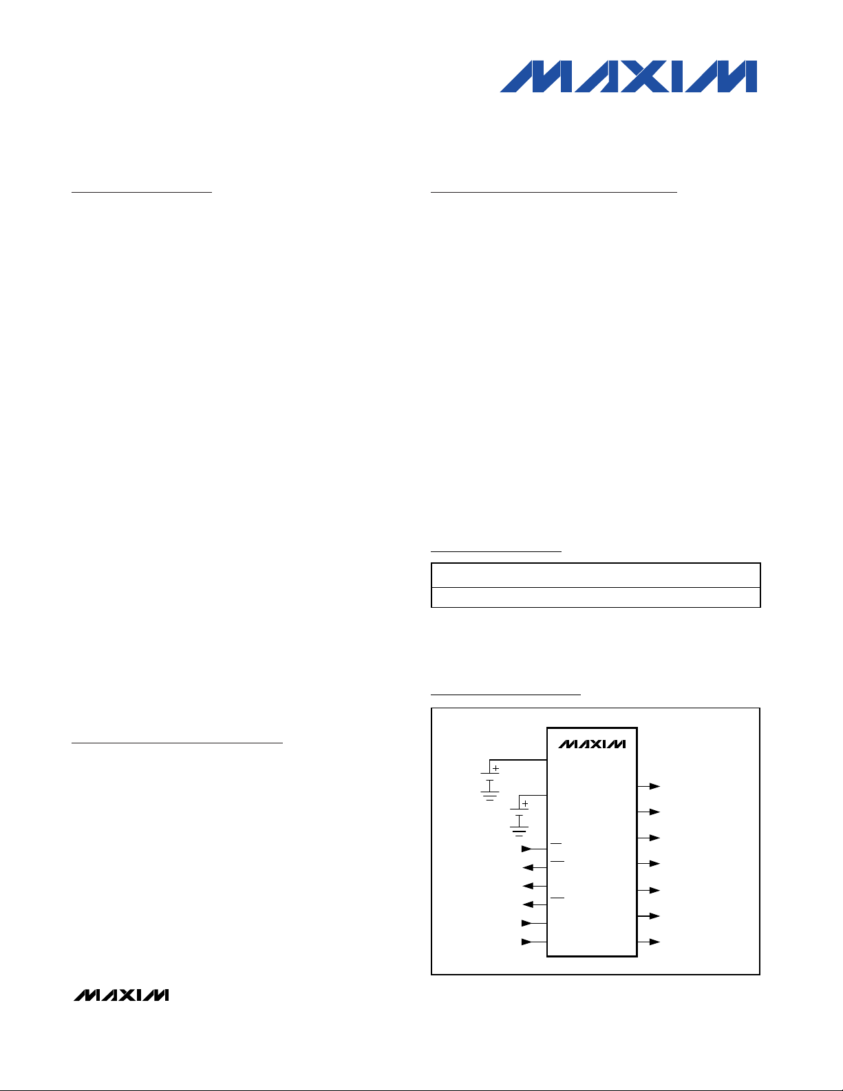
Simplified Diagram
19-3527; Rev 0; 3/05
For pricing, delivery, and ordering information, please contact Maxim/Dallas Direct! at
1-888-629-4642, or visit Maxim’s website at www.maxim-ic.com.
Pin Configuration appears at end of data sheet.
X-Scale is a trademark of Intel Corp.
Ordering Information
PART TEMP RANGE PIN-PACKAGE
MAX8588ETM -40°C to +85°C 48 Thin QFN (6mm x 6mm)
MAIN BATTERY
nRESET
nVCC_FAULT
nBATT_FAULT
SYS_EN
PWR_EN
BACKUP
BATTERY
IN
BKBT
MR
RSO
POK
DBO
ON1-2
ON3-6
MAX8588
V1
V2
V3
V4
V5
V6
V7
VCC_IO 3.3V
VCC_MEM 2.5V
VCC_CORE
0.8V TO 1.3V
VCC_PLL 1.3V
VCC_SRAM 1.1V
VCC_USIM
0V, 1.8V, 3.0V
VCC_BATT

MAX8588
High-Efficiency, Low-IQPMIC with
Dynamic Core for PDAs and Smartphones
2 _______________________________________________________________________________________
ABSOLUTE MAXIMUM RATINGS
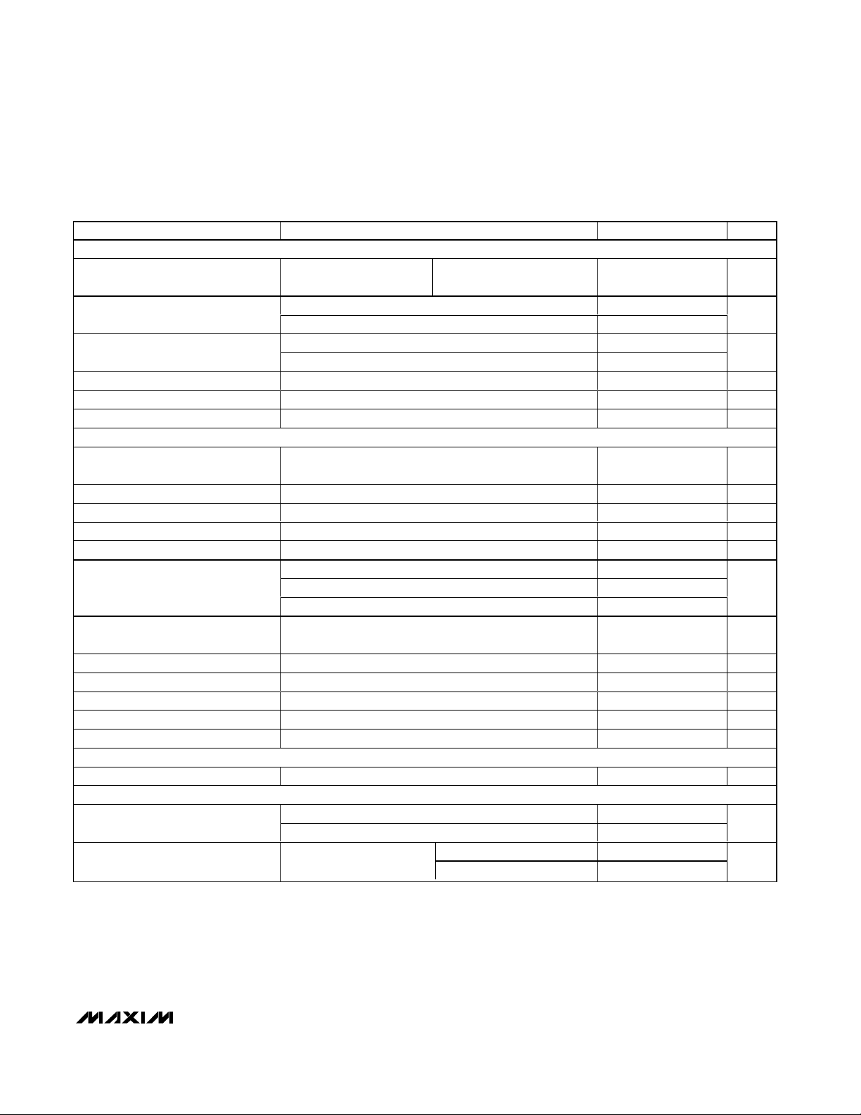
ELECTRICAL CHARACTERISTICS
(VIN= 3.6V, V
BKBT
= 3.0V, V
LBI
= 1.1V, V
DBI
= 1.35V, circuit of Figure 5, TA = 0°C to +85°C, unless otherwise noted. Typical values
are at T
A
= +25°C.)
Stresses beyond those listed under “Absolute Maximum Ratings” may cause permanent damage to the device. These are stress ratings only, and functional
operation of the device at these or any other conditions beyond those indicated in the operational sections of the specifications is not implied. Exposure to
absolute maximum rating conditions for extended periods may affect device reliability.
IN, IN45, IN6, MR, LBO, DBO, RSO, POK, SCL, SDA,
BKBT, V7, SLP, SRAD, PWM3 to GND...............-0.3V to +6V
REF, CC_, ON_, FB_, DBI, LBI, V1, V2, RAMP, BYP,
MR to GND ...........................................-0.3V to (V
IN
+ 0.3V)
PV1, PV2, PV3, SLPIN to IN...................................-0.3V to +0.3V
V4, V5 to GND ..........................................-0.3V to (V
IN45
+ 0.3V)
V6 to GND ..................................................-0.3V to (V
IN6
+ 0.3V)
PV1 to PG1 ............................................................-0.3V to +6.0V
PV2 to PG2 ............................................................-0.3V to +6.0V
PV3 to PG3 ............................................................-0.3V to +6.0V
LX1 Continuous Current....................................-1.30A to +1.30A
LX2 Continuous Current........................................-0.9A to +0.9A
LX3 Continuous Current........................................-0.5A to +0.5A
PG1, PG2, PG3 to GND.........................................-0.3V to +0.3V
V1, V2, V4, V5, V6 Output Short-Circuit Duration.......Continuous
Continuous Power Dissipation (T
A
= +70°C)
6mm x 6mm 48-Pin Thin QFN
(derate 26.3mW/°C above +70°C)...........................2105mW
Operating Temperature Range ...........................-40°C to +85°C
Junction Temperature......................................................+150°C
Storage Temperature Range .............................-65°C to +150°C
Lead Temperature (soldering, 10s) .................................+300°C
PV1, PV2, PV3, SLPIN, IN Supply
Voltage Range
IN45, IN6 Supply Voltage Range 2.4 5.5 V
IN Undervoltage-Lockout (UVLO)
Threshold
Quiescent Current
BKBT Input Current
REF Output Voltage 0 to 10µA load 1.2375 1.25 1.2625 V
SYNCHRONOUS-BUCK PWM REG1
REG1 Voltage Accuracy FB1 = GND, 3.6V ≤ V
FB1 Voltage Accuracy
FB1 Input Current FB1 used with external resistors 100 nA
Error-Amplifier Transconductance Referred to FB 87 µS
Dropout Voltage (Note 1)
PARAMETER CONDITIONS MIN TYP MAX UNITS
PV1, PV2, PV3, IN, and SLPIN must connect together
externally
V
rising 2.25 2.40 2.55
IN
falling 2.200 2.35 2.525
V
IN
+ I
PV3
PV1
+ I
IN45
+
+
IN
+
PV1
No load (I
I
+ I
PV2
I
SLPIN
I
)
IN6
ON1 = 0 4
ON1 = IN 0.8
FB1 used with external resistors, 3.6V ≤ V
load = 0 to 1300mA
Load = 800mA 180 280
Load = 1300mA 293 450
Only V7 on, V
REG1 and REG2 on in switch mode,
REG3 off
REG1 and REG2 on in sleep mode,
REG3 off
All REGs on 225
≤ 5.5V, load = 0 to 1300mA 3.25 3.3 3.35 V
= 3.0V 32
IN
≤ 5.5V,
PV1
2.6 5.5 V
130
60
1.231 1.25 1.269 V
V
µA
µA
mV

MAX8588
High-Efficiency, Low-I
Q
PMIC with
Dynamic Core for PDAs and Smartphones
_______________________________________________________________________________________ 3
ELECTRICAL CHARACTERISTICS (continued)
(VIN= 3.6V, V
BKBT
= 3.0V, V
LBI
= 1.1V, V
DBI
= 1.35V, circuit of Figure 5, TA = 0°C to +85°C, unless otherwise noted. Typical values
are at T
A
= +25°C.)
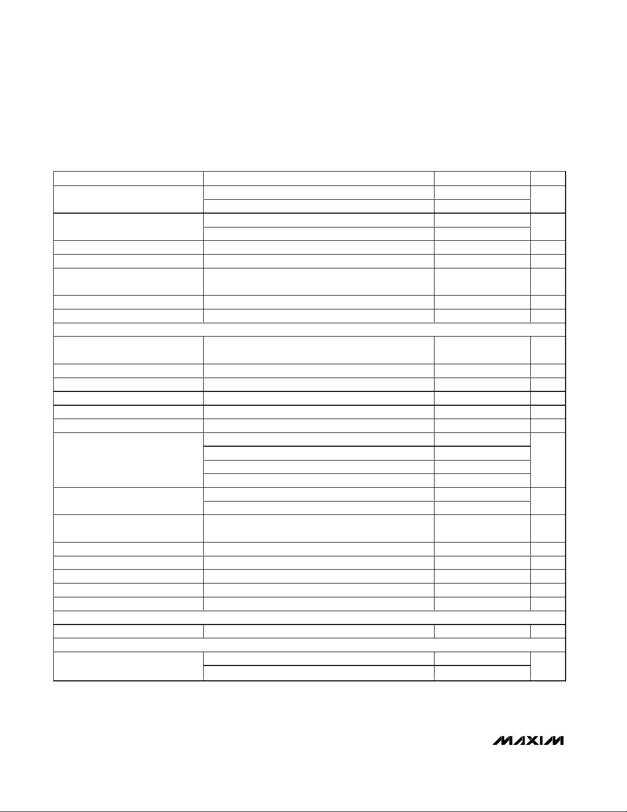
p-Channel On-Resistance
n-Channel On-Resistance
Current-Sense Transresistance 0.5 V/A
p-Channel Current-Limit Threshold -1.55 -1.80 -2.10 A
PWM Skip-Mode Transition Load
Current
OUT1 Maximum Output Current 2.6V ≤ V
LX1 Leakage Current V
SYNCHRONOUS-BUCK PWM REG2
REG2 Voltage Accuracy
FB2 Voltage Accuracy
FB2 Input Current FB2 used with external resistors, V
Error-Amplifier Transconductance Referred to FB 87 µS
Dropout Voltage Load = 900mA (Note 1) 243 380 mV
p-Channel On-Resistance
n-Channel On-Resistance
Current-Sense Transresistance 0.7 V/A
p-Channel Current-Limit Threshold -1.10 -1.275 -1.50 A
PWM Skip-Mode Transition Load
Current
OUT2 Maximum Output Current 2.6V ≤ V
LX2 Leakage Current V
SYNCHRONOUS-BUCK PWM REG3
REG3 Voltage Accuracy
Error-Amplifier Transconductance 68 µS
PARAMETER CONDITIONS MIN TYP MAX UNITS
I
= -180mA 0.18 0.3
LX1
I
= -180mA, V
LX1
I
= 180mA 0.13 0.225
LX1
I
= 180mA, V
LX1
Decreasing load current (Note 2) 30 mA
≤ 5.5V (Note 3) 1.3 A
PV1
= 5.5V, LX1 = GND or PV1, V
PV1
FB2 = GND, 3.6V ≤ V
FB2 = IN, 3.6V ≤ V
FB2 used with external resistors, 3.6V ≤ V
load = 0 to 900mA
I
= -180mA 0.225 0.375
LX2
= -180mA, V
I
LX2
I
= 180mA 0.15 0.25
LX2
= 180mA, V
I
LX2
Decreasing load current (Note 2) 30 mA
≤ 5.5V (Note 3) 0.9 A
PV2
= 5.5V, LX2 = GND or PV2, V
PV2
REG3 from 0.7V to 1.475V,
2.6V ≤ V
PV3
≤ 5.5V
= 2.6V 0.21 0.35
PV1
= 2.6V 0.15 0.25
PV1
= 0V -20 +0.1 +20 µA
ON1
≤ 5.5V, load = 0 to 900mA 2.463 2.5 2.537
PV2
≤ 5.5V, load = 0 to 900mA 3.25 3.3 3.35
PV2
≤ 5.5V,
PV2
= 1.25V 100 nA
FB2
= 2.6V 0.26 0.425
PV2
= 2.6V 0.17 0.275
PV2
= 0V -10 +0.1 +10 µA
ON2
Load = 0 to 500mA -1.5 +1.5 %
1.231 1.25 1.269 V
Ω
Ω
V
Ω
Ω
MAX8588
High-Efficiency, Low-IQPMIC with
Dynamic Core for PDAs and Smartphones
4 _______________________________________________________________________________________
ELECTRICAL CHARACTERISTICS (continued)
(VIN= 3.6V, V
BKBT
= 3.0V, V
LBI
= 1.1V, V
DBI
= 1.35V, circuit of Figure 5, TA = 0°C to +85°C, unless otherwise noted. Typical values
are at T
A
= +25°C.)
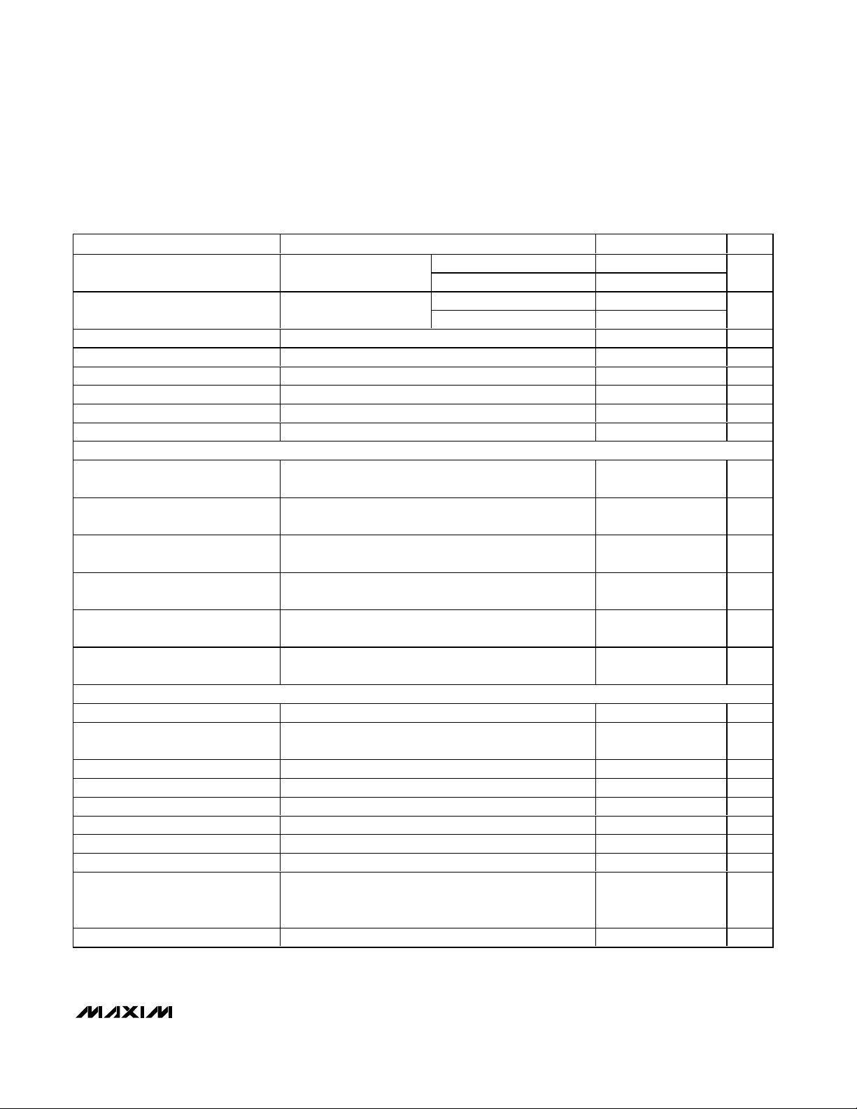
p-Channel On-Resistance
n-Channel On-Resistance
Current-Sense Transresistance 1.1 V/A
p-Channel Current-Limit Threshold -0.60 -0.7 -0.85 A
PWM Skip-Mode Transition Load
Current
OUT3 Maximum Output Current 2.6V ≤ V
LX3 Leakage Current V
LDOS V4, V5, V6, V1 SLEEP, V2 SLEEP, AND V7 OUTPUT
V4, V5, V6, V1 SLEEP, V2 SLEEP
Output Current
V7 Output Current 30 mA
REG4 Output Voltage Load = 0.1mA to 35mA 1.261 1.3 1.339 V
REG4 Noise With 1µF C
REG5 Output Voltage Load = 0.1mA to 35mA 1.067 1.1 1.133 V
IN45, IN6 Input Voltage Range 2.4 5.5 V
REG6 Output Voltage (POR Default
to 0V, Set by Serial Input)
V7 Output Voltage
V1 and V2 SLEEP Output Voltage
Accuracy
V1 and V2 SLEEP Dropout Voltage Load = 20mA 75 150 mV
V6 Dropout Voltage 3V m od e, l oad = 30m A, 2.5V m od e, l oad = 30m A 110 200 mV
V7 Switch Voltage Drop Load = 20mA, V
V4, V5, V6 Output Current Limit 40 90 mA
BKBT Leakage 1 µA
OSCILLATOR
PWM Switching Frequency 0.93 1 1.07 MHz
SUPERVISORY/MANAGEMENT FUNCTIONS
POK Trip Threshold (Note 4)
PARAMETER CONDITIONS MIN TYP MAX UNITS
I
= -180mA 0.225 0.375
LX3
I
= -180mA, V
LX2
I
= 180mA 0.15 0.25
LX3
= 180mA, V
I
LX3
Decreasing load current (Note 2) 30 mA
≤ 5.5V (Note 3) 0.5 A
PV3
= 5.5V, LX3 = GND or PV2, V
PV3
OUT
0V setti ng ( ei ther ON 6 l ow or ser i al p r og r am m ed ) 0
1.8V setting, load = 0.1mA to 35mA 1.746 1.8 1.854
2.5V setting, load = 0.1mA to 35mA 2.425 2.5 2.575
3.0V setting, load = 0.1mA to 35mA 2.91 3.0 3.09
V1 on and in regulation V
V1 off V
Set to same output voltage as REG1 and REG2 -3.0 +3.0 %
Rising 92 94.75 97
Falling 88.5 90.5 92.5
= 2.6V 0.26 0.425
PV3
= 2.6V 0.17 0.275
PV3
= 0V -10 +0.1 +10 µA
ON3
35 mA
and 0.01µF C
= V
BKBT
V1
BYP
= 3.0V 100 200 mV
15 µV
BKBT
V1
Ω
Ω
RMS
V
V
%
MAX8588
High-Efficiency, Low-I
Q
PMIC with
Dynamic Core for PDAs and Smartphones
_______________________________________________________________________________________ 5
ELECTRICAL CHARACTERISTICS (continued)
(VIN= 3.6V, V
BKBT
= 3.0V, V
LBI
= 1.1V, V
DBI
= 1.35V, circuit of Figure 5, TA = 0°C to +85°C, unless otherwise noted. Typical values
are at T
A
= +25°C.)
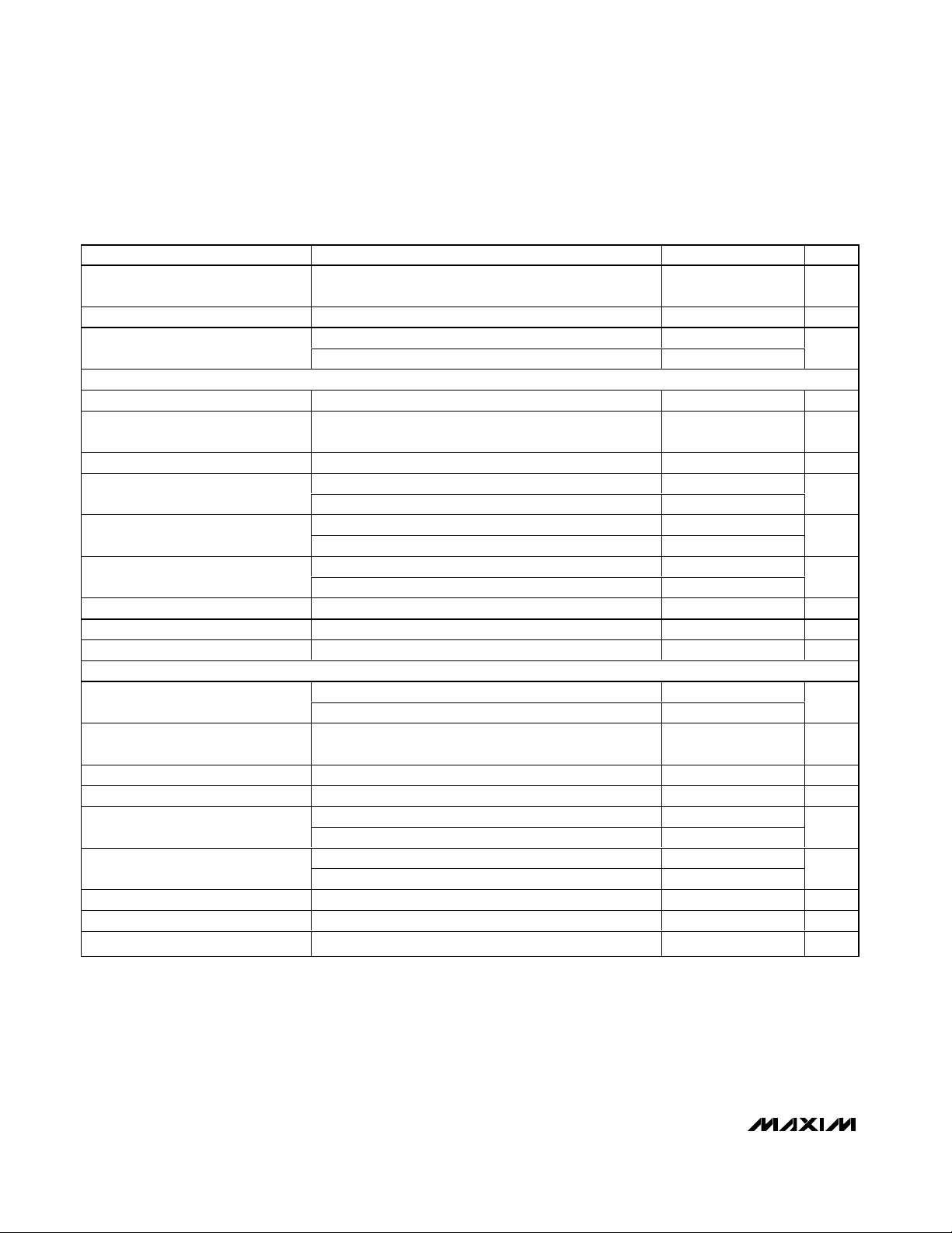
LBI Threshold (Falling) Hysteresis is 5% (typ)
DBI Threshold (Falling) Hysteresis is 5% (typ)
RSO Threshold (Falling) Voltage on REG7, hysteresis is 5% (typ) 2.25 2.41 2.56 V
RSO Deassert Delay 61 65.5 70 ms
LBI Input Bias Current -50 -5 nA
DBI Input Bias Current 15 50 nA
Thermal-Shutdown Temperature TJ rising +160 °C
Thermal-Shutdown Hysteresis 15 °C
LOGIC INPUTS AND OUTPUTS
LBO, DBO, POK, RSO, SDA Output
Low Level
LBO, DBO, POK, RSO Output Low
Level
LBO, DBO, POK, RSO Output-High
Leakage Current
ON_, SCL, SDA, SLP, PWM3, MR,
SRAD Input High Level
ON_, SCL, SDA, SLP, PWM3, MR,
SRAD Input Low Level
ON_, SCL, SDA, SLP, PWM3, MR,
SRAD Input Leakage Current
SERIAL INTERFACE
Clock Frequency 400 kHz
Bus Free Time Between START and
STOP
H ol d Ti m e Rep eated S TART C ond i ti on 0.6 µs
CLK Low Period 1.3 µs
CLK High Period 0.6 µs
S etup Ti m e Rep eated S TART C ond i ti on 0.6 µs
DATA Hold Time 0µs
DATA Setup Time 100 ns
Maximum Pulse Width of Spikes that
Must be Suppressed by the Input
Filter of Both DATA and CLK Signals
Setup Time for STOP Condition 0.6 µs
PARAMETER CONDITIONS MIN TYP MAX UNITS
LBI = IN (for preset) 3.51 3.6 3.69
With resistors at LBI 0.98 1.00 1.02
DBI = IN (for preset) 3.024 3.15 3.276
With resistors at LBI 1.208 1.232 1.256
2.6V ≤ V7
V7
Pin
2.6V ≤ V
2.6V ≤ V
Pin = GND, 5.5V -1 +1 µA
≤ 5.5V, sinking 1mA 0.4 V
= 1V, sinking 100µA 0.4 V
= 5.5V 0.2 µA
≤ 5.5V 1.6 V
IN
≤ 5.5V 0.4 V
IN
1.3 µs
50 ns
V
V
MAX8588
High-Efficiency, Low-IQPMIC with
Dynamic Core for PDAs and Smartphones
6 _______________________________________________________________________________________
ELECTRICAL CHARACTERISTICS
(VIN= 3.6V, V
BKBT
= 3.0V, V
LBI
= 1.1V, V
DBI
= 1.35V, circuit of Figure 5, TA = -40°C to +85°C, unless otherwise noted.) (Note 5)
PV1, PV2, PV3, SLPIN, IN Supply
Voltage Range
IN45, IN6 Supply Voltage Range 2.4 5.5 V
IN Undervoltage-Lockout (UVLO)
Threshold
SYNCHRONOUS-BUCK PWM REG1
REG1 Voltage Accuracy FB1 = GND, 3.6V ≤ V
FB1 Voltage Accuracy
FB1 Input Current FB1 used with external resistors 100 nA
Dropout Voltage
p-Channel On-Resistance
n-Channel On-Resistance
p-Channel Current-Limit Threshold -1.55 -2.10 A
OUT1 Maximum Output Current 2.6V ≤ V
LX1 Leakage Current V
SYNCHRONOUS-BUCK PWM REG2
REG2 Voltage Accuracy
FB2 Voltage Accuracy
FB2 Input Current FB2 used with external resistors, V
Dropout Voltage Load = 900mA (Note 1) 380 mV
p-Channel On-Resistance
n-Channel On-Resistance
p-Channel Current-Limit Threshold -1.1 -1.50 A
OUT2 Maximum Output Current 2.6V ≤ V
LX2 Leakage Current V
PARAMETER CONDITIONS MIN MAX UNITS
PV1, PV2, PV3, IN, and SLPIN must connect together
externally
V
rising 2.25 2.55
IN
V
falling 2.200 2.525
IN
≤ 5.5V, load = 0 to 1300mA 3.25 3.35 V
PV1
FB1 used with external resistors, 3.6V ≤ V
load = 0 to 1300mA
Load = 800mA (Note 1) 280
Load = 1300mA (Note 1) 450
I
= -180mA 0.3
LX1
I
= -180mA, V
LX1
I
= 180mA 0.225
LX1
I
= 180mA, V
LX1
≤ 5.5V (Note 3) 1.30 A
PV1
= 5.5V, LX1 = GND or PV1, V
PV1
FB2 = GND, 3.6V ≤ V
FB2 = IN, 3.6V ≤ V
FB2 used with external resistors, 3.6V ≤ V
load = 0 to 900mA
I
= -180mA 0.375
LX2
= -180mA, V
I
LX2
I
= -180mA 0.25
LX2
= -180mA, V
I
LX2
≤ 5.5V (Note 3) 0.9 A
PV2
= 5.5V, LX2 = GND or PV2, V
PV2
= 2.6V 0.35
PV1
= 2.6V 0.25
PV1
ON1
≤ 5.5V, load = 0 to 900mA 2.463 2.537
PV2
≤ 5.5V, load = 0 to 900mA 3.25 3.35
PV2
FB2
= 2.6V 0.425
PV2
= 2.6V 0.275
PV2
ON2
≤ 5.5V,
PV1
= 0V -10 +10 µA
≤ 5.5V,
PV2
= 1.25V 100 nA
= 0V -10 +10 µA
2.6 5.5 V
1.231 1.269 V
1.231 1.269 V
V
mV
Ω
Ω
V
Ω
Ω
MAX8588
High-Efficiency, Low-I
Q
PMIC with
Dynamic Core for PDAs and Smartphones
_______________________________________________________________________________________ 7
ELECTRICAL CHARACTERISTICS (continued)
(VIN= 3.6V, V
BKBT
= 3.0V, V
LBI
= 1.1V, V
DBI
= 1.35V, circuit of Figure 5, TA = -40°C to +85°C, unless otherwise noted.) (Note 5)
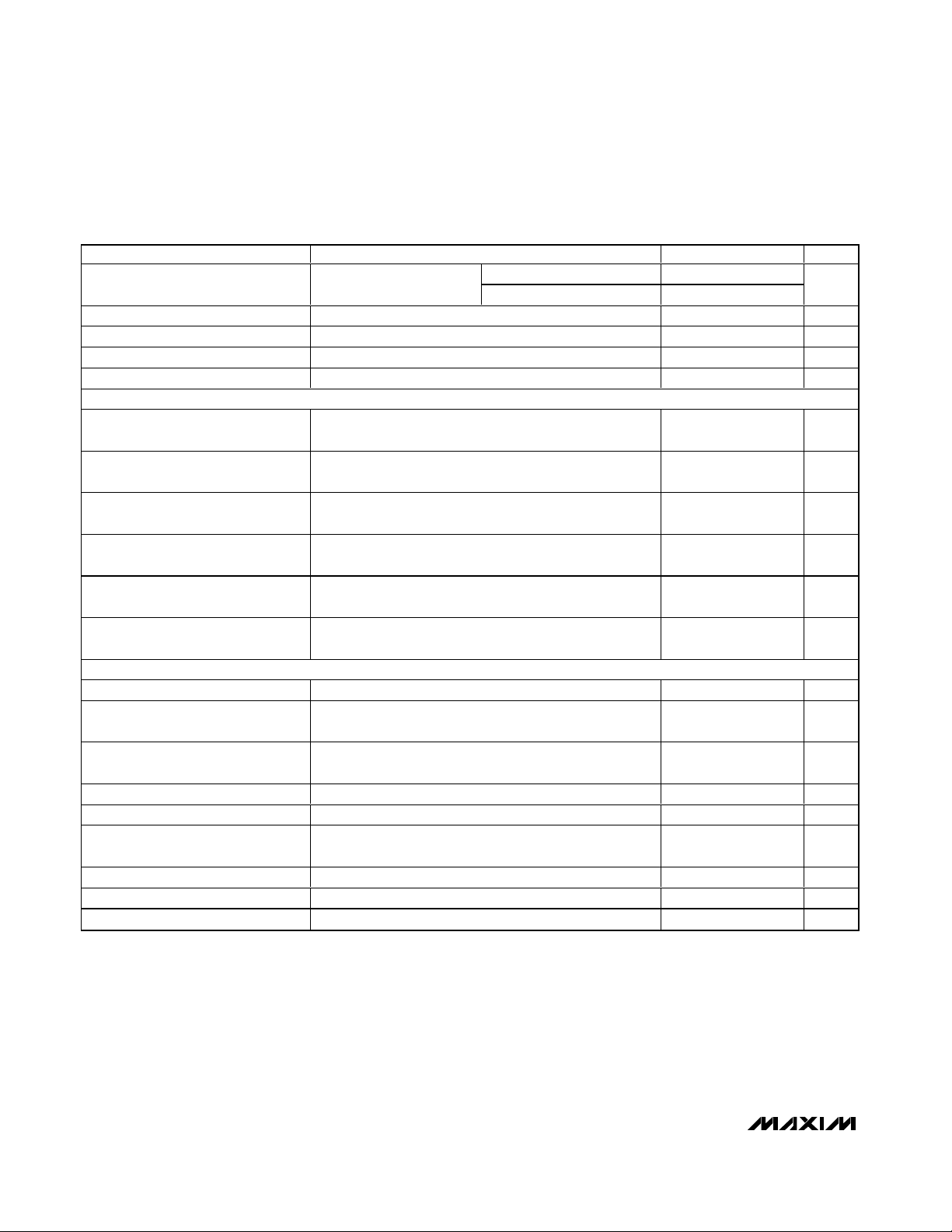
SYNCHRONOUS-BUCK PWM REG3
REG3 Output Voltage Accuracy
p-Channel On-Resistance
n-Channel On-Resistance
p-Channel Current-Limit Threshold -0.60 -0.85 A
OUT3 Maximum Output Current 2.6V ≤ V
LX3 Leakage Current V
LDOs V4, V5, V6, V1 SLEEP, V2 SLEEP, AND V7 OUTPUT
V4, V5, V6, V1 SLEEP, V2 SLEEP
Output Current
V7 Output Current 30 mA
REG4 Voltage Accuracy Load = 0.1mA to 35mA 1.254 1.346 V
REG5 Voltage Accuracy Load = 0.1mA to 35mA 1.061 1.139 V
IN45, IN6 Input Voltage Range 2.4 5.5 V
REG6 Output Voltage (POR Default
to 0V, Set by Serial Input)
V1 and V2 SLEEP Output Voltage
Accuracy
V1 and V2 SLEEP Dropout Voltage Load = 20mA 150 mV
V6 Dropout Voltage 3V m od e, l oad = 30m A; 2.5V m od e, l oad = 30m A 200 mV
V7 Switch Voltage Drop Load = 20mA, V
V4, V5, V6 Output Current Limit 40 mA
BKBT Leakage 1 µA
OSCILLATOR
PWM Switching Frequency 0.93 1.07 MHz
SUPERVISORY/MANAGEMENT FUNCTIONS
POK Trip Threshold (Note 4)
LBI Threshold (Falling) Hysteresis is 5% (typ)
PARAMETER CONDITIONS MIN MAX UNITS
REG3 from 0.7V to 1.475V,
2.6V ≤ V
I
LX3
I
LX2
I
LX3
I
LX3
PV3
1.8V setting, load = 0.1mA to 35mA 1.737 1.863
2.5V setting, load = 0.1mA to 35mA 2.412 2.588
3.0V setting, load = 0.1mA to 35mA 2.895 3.105
Set to same output voltage as REG1 and REG2 -3.5 +3.5 %
Rising 92 97
Falling 88.5 92.5
≤ 5.5V
PV3
= -180mA 0.375
= -180mA, V
= 180mA 0.25
= 180mA, V
≤ 5.5V (Note 3) 0.5 A
PV3
= 5.5V, LX3 = GND or PV2, V
= 2.6V 0.425
PV3
= 2.6V 0.275
PV3
BKBT
Load = 0 to 500mA -1.5 +1.5 %
= 0V -10 +10 µA
ON3
35 mA
= V
= 3.0V 200 mV
V1
LBI = IN (for preset) 3.51 3.69
With resistors at LBI 0.98 1.02
Ω
Ω
V
%
V
MAX8588
High-Efficiency, Low-IQPMIC with
Dynamic Core for PDAs and Smartphones
8 _______________________________________________________________________________________
ELECTRICAL CHARACTERISTICS (continued)
(VIN= 3.6V, V
BKBT
= 3.0V, V
LBI
= 1.1V, V
DBI
= 1.35V, circuit of Figure 5, TA = -40°C to +85°C, unless otherwise noted.) (Note 5)
DBI Threshold (Falling) Hysteresis is 5% (typ)
RSO Threshold (Falling) Voltage on REG7, hysteresis is 5% (typ) 2.25 2.60 V
RSO Deassert Delay 62 69 ms
LBI Input Bias Current -50 nA
DBI Input Bias Current 75 nA
LOGIC INPUTS AND OUTPUTS
LBO, DBO, POK, RSO, SDA Output
Low Level
LBO, DBO, POK, RSO, SDA Output
Low Level
LBO, DBO, POK, RSO Output-High
Leakage Current
ON_, SCL, SDA, SLP, PWM3, MR,
SRAD Input High Level
ON_, SCL, SDA, SLP, PWM3, MR,
SRAD Input Low Level
ON_, SCL, SDA, SLP, PWM3, MR,
SRAD Input Leakage Current
SERIAL INTERFACE
Clock Frequency 400 kHz
Bus Free Time Between START and
STOP
Hold Time Repeated START
Condition
CLK Low Period 1.3 µs
CLK High Period 0.6 µs
Setup Time Repeated START
Condition
DATA Hold Time 0µs
DATA Setup Time 100 ns
Setup Time for STOP Condition 0.6 µs
PARAMETER CONDITIONS MIN MAX UNITS
DBI = IN (for preset) 2.993 3.307
With resistors at LBI 1.208 1.256
2.6V ≤ V7
V7
Pin
2.6V ≤ V
2.6V ≤ V
Pin = GND, 5.5V -1 +1 µA
≤ 5.5V, sinking 1mA 0.4 V
= 1V, sinking 100µA 0.4 V
= 5.5V 0.2 µA
≤ 5.5V 1.6 V
IN
≤ 5.5V 0.4 V
IN
1.3 µs
0.6 µs
0.6 µs
V

MAX8588
High-Efficiency, Low-I
Q
PMIC with
Dynamic Core for PDAs and Smartphones
_______________________________________________________________________________________ 9
Note 1: Dropout voltage is guaranteed by the p-channel switch resistance and assumes a maximum inductor resistance of 45mΩ.
Note 2: The PWM-skip-mode transition has approximately 10mA of hysteresis.
Note 3: The maximum output current is guaranteed by the following equation:
where:
and R
N
= n-channel synchronous rectifier R
DS(ON)
RP = p-channel power switch R
DS(ON)
RL = external inductor ESR
I
OUT(MAX)
= maximum required load current
f = operating frequency minimum
L = external inductor value
I
LIM
can be substituted for I
OUT(MAX)
(desired) when solving for D. This assumes that the inductor ripple current is
small relative to the absolute value.
Note 4: POK only indicates the status of supplies that are enabled (except V7). When a supply is turned off, POK does not trigger
low. When a supply is turned on, POK immediately goes low until that supply reaches regulation. POK is forced low when all
supplies (except V7) are disabled.
Note 5: Specifications to -40°C are guaranteed by design, not production tested.
ELECTRICAL CHARACTERISTICS (continued)
VD
()
−
1
I
LIM
I
OUT
=
max
++
1
VI RR
++
OUT OUT MAX N L
D
=
VI RR
+−
IN OUT MAX N P
OUT
−
xfxL
2
()
−
RR
()
NL
()
()
1
xfxL
2
()
()
D
MAX8588
High-Efficiency, Low-IQPMIC with
Dynamic Core for PDAs and Smartphones
10 ______________________________________________________________________________________
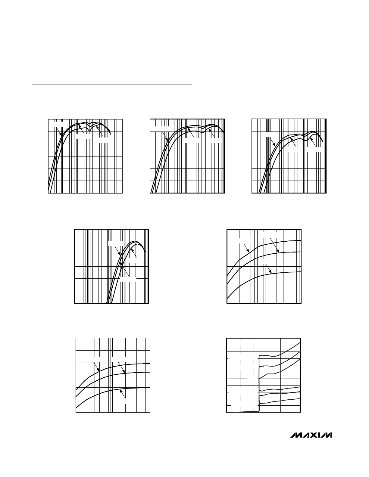
Typical Operating Characteristics
(Circuit of Figure 6, V
IN
= 3.6V, TA = +25°C, unless otherwise noted.)
100
0.1 1 10 100 1000 10,000
90
80
70
60
50
40
REG1 3.3V OUTPUT EFFICIENCY
vs. LOAD CURRENT
MAX8588 toc01
LOAD CURRENT (mA)
EFFICIENCY (%)
VIN = 3.6V
VIN = 4.0V
VIN = 5.0V
100
40
0.1 10 1001 1000
REG2 2.5V OUTPUT EFFICIENCY
vs. LOAD CURRENT
MAX8588 toc02
LOAD CURRENT (mA)
EFFICIENCY (%)
50
60
70
80
90
VIN = 3.6V
VIN = 4.0V
VIN = 5.0V
100
40
0.1 10 1001 1000
REG3 1.3V OUTPUT EFFICIENCY
vs. LOAD CURRENT
MAX8588 toc03
LOAD CURRENT (mA)
EFFICIENCY (%)
50
60
70
80
90
VIN = 3.6V
VIN = 4.0V VIN = 5.0V
0.1 10 1001 1000
REG3 1.3V OUTPUT WITH FORCED-PWM
EFFICIENCY vs. LOAD CURRENT
MAX8588 toc04
LOAD CURRENT (mA)
EFFICIENCY (%)
VIN = 3.6V
VIN = 5.0V
VIN = 4.0V
100
40
50
60
70
80
90
REG2 SLEEP LDO 2.5V OUTPUT
EFFICIENCY vs. LOAD CURRENT
MAX8588 toc06
LOAD CURRENT (mA)
EFFICIENCY (%)
90
30
40
50
60
70
80
0.1 1 10
VIN = 3.6V VIN = 4.0V
VIN = 5.0V
REG1 SLEEP LDO 3.3V OUTPUT
EFFICIENCY vs. LOAD CURRENT
MAX8588 toc05
LOAD CURRENT (mA)
EFFICIENCY (%)
100
40
50
60
70
80
90
0.1 1 10
VIN = 3.6V
VIN = 4.0V
VIN = 5.0V
0
20
140
100
180
220
021345
QUIESCENT CURRENT
vs. SUPPLY VOLTAGE
MAX8588 toc07
INPUT VOLTAGE (V)
INPUT CURRENT (µA)
BKBT BIASED AT 3.6V
V1, V2, AND V3 ON
V1 AND V2 ON
V1 ON
V1 AND V2 SLEEP
V1 SLEEP
ALL BUT V7 OFF
200
160
40
60
80
120
 Loading...