Maxim MAX8586ETA, MAX8586ETA/V Schematic [ru]

General Description
The MAX8586 single current-limited switch controls up to
1.2A to power USB applications and has multiple protection features including thermal shutdown, internal current
limiting, and reverse current protection. The thermal shutdown limits junction temperature during a prolonged
short or overload condition. The internal current-limiting
circuitry protects the input supply against overload and
is programmable using an external resistor. The
MAX8586 meets all IEC specifications for USB ports.
The IC latches off when the output experiences a short
circuit for more than 20ms, saving system power. Autorestart tests the shorted output with a 25mA current to
determine if the short still exists. Once the short is
removed, the MAX8586 automatically restarts the output. An open-drain fault signal notifies the system that
the internal current limit has been reached. A 20ms
fault-blanking feature allows the circuit to ignore
momentary faults such as those caused when hotswapping into a capacitive load. An ENRESET input is
available to disable the auto-restart function.
The MAX8586 features a SEL input that programs ON
to be either active high or active low. The IC is supplied
in a space-saving, 8-pin, 3mm x 3mm TDFN package.
Features
♦ Reverse Current Protection
♦ Programmable Current Limit Up to 1.2A
♦ Accurate Current Limit
♦ Selectable Auto-Restart when Fault Is Removed
♦ Thermal-Overload Protection
♦ Selectable Active-High/Low ON Input
♦ Built-In 20ms Fault Blanking
♦ Compliant with All USB Specifications
♦ 2.75V to 5.5V Input Supply Range
♦ FAULT Indicator Output
♦ 15kV ESD Protection (with Caps)
♦ Tiny 8-Pin 3mm x 3mm TDFN Package
Applications
USB Ports/Hubs
Desktop/Notebook Computers
PDAs and Palmtop Computers
Docking Stations
Single 1.2A USB Switch in
3mm x 3mm TDFN
MAX8586
For pricing, delivery, and ordering information, please contact Maxim Direct at
1-888-629-4642, or visit Maxim Integrated’s website at www.maximintegrated.com.
EVALUATION KIT AVAILABLE
Pin Configuration appears at end of data sheet.
Ordering Information
19-3449; Rev 3; 1/13
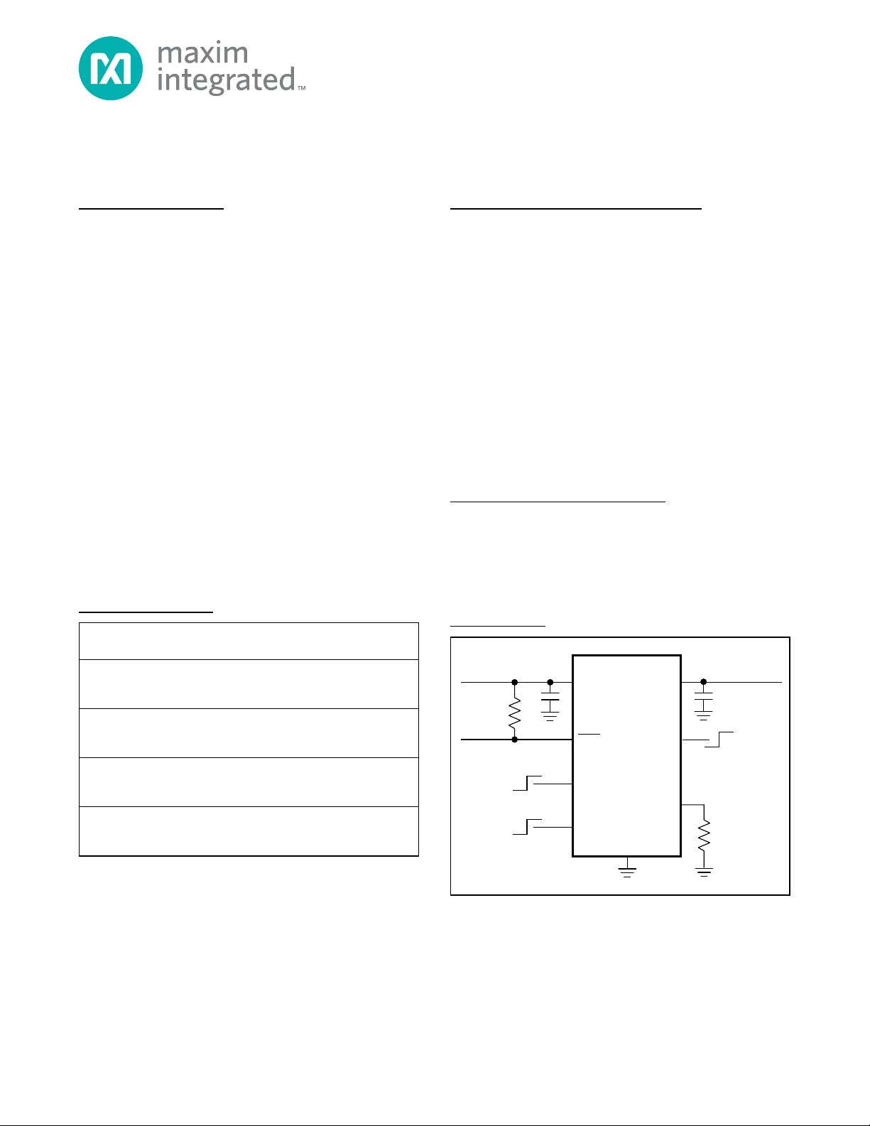
Typical Operating Circuit
/V denotes an automotive qualified part.
+
Denotes a lead(Pb)-free/RoHS-compliant package.
T = Tape and reel.
PART TEMP RANGE
MAX8586ETA -40° C to +85° C
MAX8586ETA+ -40°C to +85°C
MAX8586ETA+T -40° C to +85° C
MAX8586ETA/V+ -40° C to +85°C
PIN-
PACKAGE
8 TDFN
3mm x 3mm
(T833-2)
8 TDFN
3mm x 3mm
(T833-2)
8 TDFN
3mm x 3mm
(T833-2)
8 TDFN
3mm x 3mm
(T833-2)
TOP
MARK
AMH
AMH
AMH
BLU
INPUT SUPPLY
2.75V TO 5.5V
OUTPUT
FAULT
INDICATOR
ON/OFF
POLARITY
SELECTION
ON/OFF
CONTROL
IN OUT
MAX8586
FAULT
SEL
ON
ENRESET
ISET
GND
OUTPUT SUPPLY
UP TO 1.2A
AUTO-RESTART
ON/OFF

Single 1.2A USB Switch in
3mm x 3mm TDFN
2 Maxim Integrated
MAX8586
ABSOLUTE MAXIMUM RATINGS
ELECTRICAL CHARACTERISTICS
(VIN= VON= V
SEL
= V
ENRESET
= 5V, R
ISET
= 26kΩ to GND, R
FAULT
= 100kΩ pullup to VIN, C
OUT
= 0.1µF, TA= -40°C to +85°C.
Typical values are at T
A
= +25°C, unless otherwise specified.) (Note 1)
Stresses beyond those listed under “Absolute Maximum Ratings” may cause permanent damage to the device. These are stress ratings only, and functional
operation of the device at these or any other conditions beyond those indicated in the operational sections of the specifications is not implied. Exposure to
absolute maximum rating conditions for extended periods may affect device reliability.
IN, ON, SEL, OUT, FAULT, ISET, ENRESET to GND ..-0.3V to +6V
IN to OUT.....................................................................-6V to +6V
FAULT Sink Current ............................................................20mA
Continuous Power Dissipation
8-Pin 3mm x 3mm TDFN
(derate 24mW/°C above +70°C)................................1951mW
Operating Temperature Range ...........................-40°C to +85°C
Junction Temperature......................................................+150°C
Storage Temperature Range .............................-65°C to +150°C
Soldering Temperature (reflow) .......................................+260°C
Supply Voltage Range 2.75 5.50 V
IN Standby Supply Current VON = 0V 3 6 µA
IN Quiescent Supply Current I
OUT Off-Leakage Current VON = 0V, V
Undervoltage-Lockout Threshold Rising edge, 3% hysteresis (typ) 2.3 2.5 2.7 V
RMS Short-Circuit Current Limit
Short-Circuit/Continuous Current Limit
Transition Threshold
Fault-Blanking Timeout Period From current-limit condition to FAULT falling 8 20 40 ms
PARAMETER CONDITIONS MIN TYP MAX UNITS
VIN = 5V 55
VIN = 3V 65Switch On-Resistance
V
IN
OUT
R
ISET
R
ISET
R
ISET
V
OUT
(I
OUT
V
OUT
(I
OUT
(Note 2) 1 V
= 4.4V 95
= 0A 30 55 µA
= 26kΩ 1.2 1.4 1.6
= 39kΩ 0.800 0.925 1.050Current-Limit Threshold
= 60kΩ 0.5 0.6 0.7
= 0V,
pulsing)
= 0V,
pulsing)
OUT
= 0V
TA = +25°C 0.02 1
= +85°C 0.6
T
A
R
ISET
R
ISET
R
ISET
R
ISET
R
ISET
R
ISET
= 26kΩ 1.35 1.75 2.20
= 39kΩ 1.2Peak Short-Circuit Current Limit
= 60kΩ 0.74
= 26kΩ 0.55
= 39kΩ 0.37
= 60kΩ 0.23
mΩ
µA
A
A (Peak)
A (RMS)

Single 1.2A USB Switch in
3mm x 3mm TDFN
Maxim Integrated 3
MAX8586
ELECTRICAL CHARACTERISTICS (continued)
(VIN= VON= V
SEL
= V
ENRESET
= 5V, R
ISET
= 26kΩ to GND, R
FAULT
= 100kΩ pullup to VIN, C
OUT
= 0.1µF, TA= -40°C to +85°C.
Typical values are at T
A
= +25°C, unless otherwise specified.) (Note 1)
Note 1: All devices are 100% production tested at T
A
= +25°C. Limits over the operating temperature range are guaranteed by
design.
Note 2: The output voltage at which the device transitions from short-circuit current limit to continuous current limit.
Turn-On Delay
Output Rise Time
Turn-Off Delay from ON
Output Fall Time
Thermal-Shutdown Threshold 15°C hysteresis (typ) +160 °C
ON, SEL, ENRESET Logic Input High Voltage
ON, SEL, ENRESET Logic Input Low Voltage
Logic Input Current TA = +25°C-1+1µA
FAULT Output Low Voltage I
FAULT Output High Leakage Current VIN = 5.5V, TA = +25°C1µA
ISET Current-Limit Trip Point R
ISET External Resistance Range 26 60 kΩ
Auto-Restart Current In latched-off state, V
Auto-Restart Threshold In latched-off state, V
Auto-Restart Delay In latched-off state, V
PARAMETER CONDITIONS MIN TYP MAX UNITS
R
OUT
ON rising to 10% of V
rise time
R
OUT
10% to 90% of V
R
OUT
ON falling to 90% of V
R
OUT
90% to 10% of V
VIN = 2.75V to 4.0V 1.6
V
IN
VIN = 2.75V to 4.0V 0.6
V
IN
SINK
ISET
= 10Ω, C
= 10Ω, C
= 10Ω, C
= 10Ω, C
= 4.0V to 5.5V 2.0
= 4.0V to 5.5V 0.8
= 1mA 0.4 V
= 26kΩ 600 mV
= 1µF, measured from
OUT
OUT
OUT
OUT
OUT
OUT
, does not include
OUT
= 1µF, measured from
= 1µF measured from
OUT
= 1µF, measured from
= 0V 10 25 60 mA
OUT
rising 0.4 0.5 0.6 V
OUT
>1V 8 20 40 ms
OUT
0.5 1.5 4.0 ms
5.5 ms
100 1000 µs
4ms
V
V

Single 1.2A USB Switch in
3mm x 3mm TDFN
4 Maxim Integrated
MAX8586
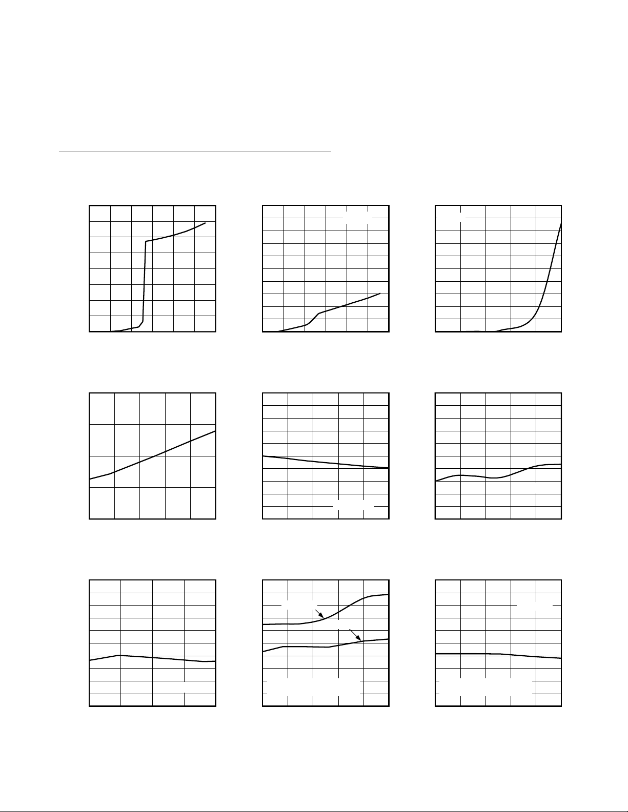
Typical Operating Characteristics
(Typical Application Circuit, VIN= VON= V
SEL
= V
ENRESET
= 5V, TA= +25°C, unless otherwise noted.)
QUIESCENT SUPPLY CURRENT
vs. SUPPLY VOLTAGE
40
35
30
25
20
15
SUPPLY CURRENT (μA)
10
5
0
06
SUPPLY VOLTAGE (V)
541 2 3
MAX8586 toc01
SHUTDOWN SUPPLY CURRENT
vs. SUPPLY VOLTAGE
10
9
8
7
6
5
4
3
SUPPLY CURRRENT (μA)
2
1
0
06
SUPPLY VOLTAGE (V)
VON = 0V
SWITCH LEAKAGE CURRENT
vs. TEMPERATURE
0.50
VON = 0V
0.45
MAX8586 toc02
0.40
0.35
0.30
0.25
0.20
0.15
LEAKAGE CURRENT (μA)
0.10
0.05
0
54321
-40 85
TEMPERATURE (°C)
603510-15
MAX8586 toc03
NORMALIZED ON-RESISTANCE
vs. TEMPERATURE
1.50
1.25
ON
1.00
NORMALIZED R
0.75
0.50
-40 85
TEMPERATURE (°C)
CURRENT LIMIT
vs. INPUT VOLTAGE
2.0
1.9
1.8
1.7
1.6
1.5
1.4
CURRENT LIMIT (A)
1.3
1.2
1.1
1.0
2.7 5.5
INPUT VOLTAGE (V)
V
ENRESET
4.13.4
CONTINUOUS CURRENT LIMIT
vs. TEMPERATURE
MAX8586 toc05
CURRENT LIMIT (A)
1.50
1.48
1.46
1.44
1.42
1.40
1.38
1.36
1.34
1.32
1.30
-40 85
1.60
1.58
MAX8586 toc04
1.56
1.54
1.52
1.50
1.48
CURRENT LIMIT (A)
1.46
1.44
V
= 0V
1.42
1.40
603510-15
-40 85
TEMPERATURE (°C)
ENRESET
603510-15
SWITCH ON-TIME
vs. TEMPERATURE
9.0
8.5
MAX8586 toc07
8.0
7.5
7.0
6.5
6.0
ON-TIME (ms)
5.5
= 5V
4.8
5.0
4.5
4.0
R
= 5Ω
LOAD
NO LOAD
MEASURED FROM ON HIGH UNTIL
REACHES 90% OF THE INPUT
V
OUT
-40 85
TEMPERATURE (°C)
603510-15
10
9
MAX8586 toc08
8
7
6
5
4
3
OUTPUT FALL TIME (ms)
2
1
0
MEASURED FROM ON LOW UNTIL
V
-40 85
CURRENT LIMIT
vs. TEMPERATURE
TEMPERATURE (°C)
SWITCH OFF-TIME
vs. TEMPERATURE
FALLS TO 10% OF THE INPUT
OUT
TEMPERATURE (°C)
V
ENRESET
R
LOAD
603510-15
603510-15
= 5V
= 5Ω
MAX8586 toc06
MAX8586 toc09

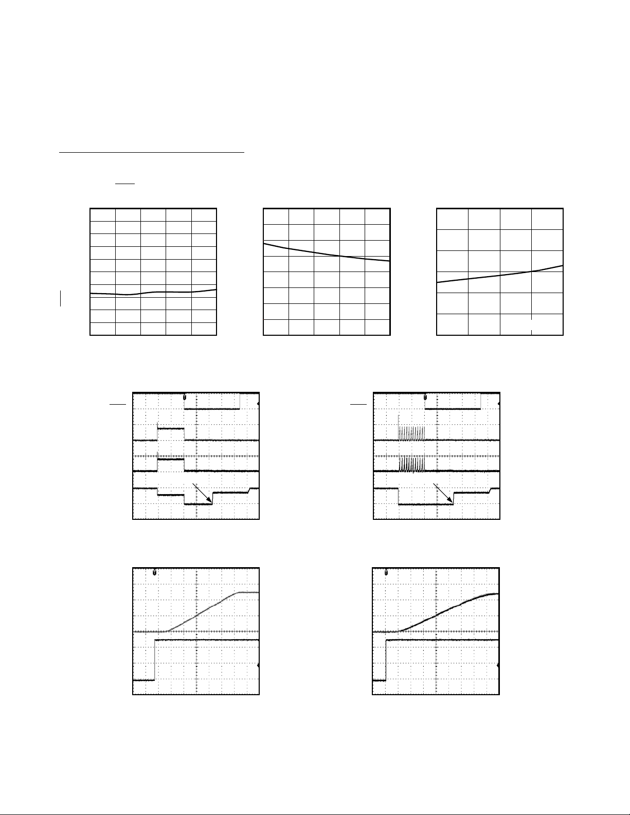
Typical Operating Characteristics (continued)
(Typical Application Circuit, VIN= VON= V
SEL
= V
ENRESET
= 5V, TA= +25°C, unless otherwise noted.)
Single 1.2A USB Switch in
3mm x 3mm TDFN
Maxim Integrated 5
MAX8586
FAULT-BLANKING TIME
vs. TEMPERATURE
35
33
31
29
27
25
23
21
FAULT-BLAMKING TIME (ms)
19
17
15
-40 85
TEMPERATURE (°C)
OVERLOAD RESPONSE INTO 2Ω
FAULT
I
IN
I
OUT
V
OUT
FAULT REMOVED
AUTO-RESTART CURRENT
vs. TEMPERATURE
28
27
MAX8586 toc10
26
25
24
23
22
AUTO-RESTART CURRENT (mA)
21
MAX8586 toc13
20
TEMPERATURE (°C)
603510-15-40 85
OVERLOAD RESPONSE INTO SHORT CIRCUIT
5V/div
2A/div
2A/div
5V/div
FAULT
I
OUT
V
OUT
I
IN
603510-15
40
35
MAX8586 toc11
30
25
20
AUTO-RESTART CURRENT (mA)
15
10
FAULT REMOVED
AUTO-RESTART CURRENT
vs. INPUT VOLTAGE
R
= 0.5Ω
LOAD
2.7 5.5
INPUT VOLTAGE (V)
MAX8586 toc14
4.84.13.4
5V/div
2A/div
2A/div
5V/div
MAX8586 toc12
10ms/div
SWITCH TURN-ON WAVEFORM INTO NO LOAD
V
OUT
V
ON
1ms/div
MAX8586 toc15
2V/div
2V/div
SWITCH TURN-ON WAVEFORM INTO 5Ω LOAD
V
OUT
V
ON
10ms/div
MAX8586 toc16
2V/div
2V/div
1ms/div
 Loading...