

General Description
The MAX8586 single current-limited switch controls up to
1.2A to power USB applications and has multiple protection features including thermal shutdown, internal current
limiting, and reverse current protection. The thermal shutdown limits junction temperature during a prolonged
short or overload condition. The internal current-limiting
circuitry protects the input supply against overload and
is programmable using an external resistor. The
MAX8586 meets all IEC specifications for USB ports.
The IC latches off when the output experiences a short
circuit for more than 20ms, saving system power. Autorestart tests the shorted output with a 25mA current to
determine if the short still exists. Once the short is
removed, the MAX8586 automatically restarts the output. An open-drain fault signal notifies the system that
the internal current limit has been reached. A 20ms
fault-blanking feature allows the circuit to ignore
momentary faults such as those caused when hotswapping into a capacitive load. An ENRESET input is
available to disable the auto-restart function.
The MAX8586 features a SEL input that programs ON
to be either active high or active low. The IC is supplied
in a space-saving, 8-pin, 3mm x 3mm TDFN package.
Applications
USB Ports/Hubs
Desktop/Notebook Computers
PDAs and Palmtop Computers
Docking Stations
Features
o Reverse Current Protection
o Programmable Current Limit Up to 1.2A
o Accurate Current Limit
o Selectable Auto-Restart when Fault Is Removed
o Thermal-Overload Protection
o Selectable Active-High/Low ON Input
o Built-In 20ms Fault Blanking
o Compliant with All USB Specifications
o 2.75V to 5.5V Input Supply Range
o FAULT Indicator Output
o 15kV ESD Protection (with Caps)
o Tiny 8-Pin 3mm x 3mm TDFN Package
MAX8586
Single 1.2A USB Switch in
3mm x 3mm TDFN
________________________________________________________________
Maxim Integrated Products
1
Pin Configuration appears at end of data sheet.
Ordering Information
19-3449; Rev 2; 1/10
EVALUATION KIT
AVAILABLE
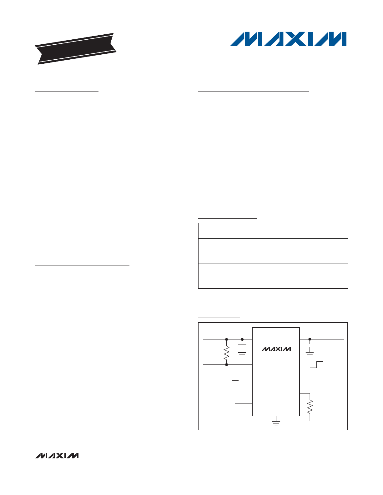
Typical Operating Circuit
/V denotes an automotive qualified part.
+
Denotes a lead(Pb)-free/RoHS-compliant package.
For pricing, delivery, and ordering information, please contact Maxim Direct at 1-888-629-4642,
or visit Maxim's website at www.maxim-ic.com.
PART TEMP RANGE
MAX8586ETA -40°C to +85°C
MAX8586ETA/V+ -40°C to +85°C
PIN-
PACKAGE
8 TDFN
3mm x 3mm
(T833-2)
8 TDFN
3mm x 3mm
(T833-2)
TOP
MARK
AMH
BLU
INPUT SUPPLY
2.75V TO 5.5V
OUTPUT
FAULT
INDICATOR
ON/OFF
POLARITY
SELECTION
ON/OFF
CONTROL
IN OUT
MAX8586
FAULT
SEL
ON
ENRESET
ISET
GND
OUTPUT SUPPLY
UP TO 1.2A
AUTO-RESTART
ON/OFF
MAX8586
Single 1.2A USB Switch in
3mm x 3mm TDFN
2 _______________________________________________________________________________________
ABSOLUTE MAXIMUM RATINGS
ELECTRICAL CHARACTERISTICS
(VIN= VON= V
SEL
= V
ENRESET
= 5V, R
ISET
= 26kΩ to GND, R
FAULT
= 100kΩ pullup to VIN, C
OUT
= 0.1µF, TA= -40°C to +85°C.
Typical values are at T
A
= +25°C, unless otherwise specified.) (Note 1)
Stresses beyond those listed under “Absolute Maximum Ratings” may cause permanent damage to the device. These are stress ratings only, and functional
operation of the device at these or any other conditions beyond those indicated in the operational sections of the specifications is not implied. Exposure to
absolute maximum rating conditions for extended periods may affect device reliability.
IN, ON, SEL, OUT, FAULT, ISET, ENRESET to GND ..-0.3V to +6V
IN to OUT.....................................................................-6V to +6V
FAULT Sink Current ............................................................20mA
Continuous Power Dissipation
8-Pin 3mm x 3mm TDFN
(derate 24mW/°C above +70°C)................................1951mW
Operating Temperature Range ...........................-40°C to +85°C
Junction Temperature......................................................+150°C
Storage Temperature Range .............................-65°C to +150°C
Soldering Temperature (reflow) .......................................+260°C
Supply Voltage Range 2.75 5.50 V
IN Standby Supply Current VON = 0V 3 6 µA
IN Quiescent Supply Current I
OUT Off-Leakage Current VON = 0V, V
Undervoltage-Lockout Threshold Rising edge, 3% hysteresis (typ) 2.3 2.5 2.7 V
RMS Short-Circuit Current Limit
Short-Circuit/Continuous Current Limit
Transition Threshold
Fault-Blanking Timeout Period From current-limit condition to FAULT falling 8 20 40 ms
PARAMETER CONDITIONS MIN TYP MAX UNITS
VIN = 5V 55
VIN = 3V 65Switch On-Resistance
V
IN
OUT
R
ISET
R
ISET
R
ISET
V
OUT
(I
OUT
V
OUT
(I
OUT
(Note 2) 1 V
= 4.4V 95
= 0A 30 55 µA
= 26kΩ 1.2 1.4 1.6
= 39kΩ 0.800 0.925 1.050Current-Limit Threshold
= 60kΩ 0.5 0.6 0.7
= 0V,
pulsing)
= 0V,
pulsing)
OUT
= 0V
TA = +25°C 0.02 1
= +85°C 0.6
T
A
R
ISET
R
ISET
R
ISET
R
ISET
R
ISET
R
ISET
= 26kΩ 1.35 1.75 2.20
= 39kΩ 1.2Peak Short-Circuit Current Limit
= 60kΩ 0.74
= 26kΩ 0.55
= 39kΩ 0.37
= 60kΩ 0.23
mΩ
µA
A
A (Peak)
A (RMS)
MAX8586
Single 1.2A USB Switch in
3mm x 3mm TDFN
_______________________________________________________________________________________
3
ELECTRICAL CHARACTERISTICS (continued)
(VIN= VON= V
SEL
= V
ENRESET
= 5V, R
ISET
= 26kΩ to GND, R
FAULT
= 100kΩ pullup to VIN, C
OUT
= 0.1µF, TA= -40°C to +85°C.
Typical values are at T
A
= +25°C, unless otherwise specified.) (Note 1)
Note 1: All devices are 100% production tested at T
A
= +25°C. Limits over the operating temperature range are guaranteed by
design.
Note 2: The output voltage at which the device transitions from short-circuit current limit to continuous current limit.
Turn-On Delay
Output Rise Time
Turn-Off Delay from ON
Output Fall Time
Thermal-Shutdown Threshold 15°C hysteresis (typ) +160 °C
ON, SEL, ENRESET Logic Input High Voltage
ON, SEL, ENRESET Logic Input Low Voltage
Logic Input Current TA = +25°C-1+1µA
FAULT Output Low Voltage I
FAULT Output High Leakage Current VIN = 5.5V, TA = +25°C1µA
ISET Current-Limit Trip Point R
ISET External Resistance Range 26 60 kΩ
Auto-Restart Current In latched-off state, V
Auto-Restart Threshold In latched-off state, V
Auto-Restart Delay In latched-off state, V
PARAMETER CONDITIONS MIN TYP MAX UNITS
R
OUT
ON rising to 10% of V
rise time
R
OUT
10% to 90% of V
R
OUT
ON falling to 90% of V
R
OUT
90% to 10% of V
VIN = 2.75V to 4.0V 1.6
V
IN
VIN = 2.75V to 4.0V 0.6
V
IN
SINK
ISET
= 10Ω, C
= 10Ω, C
= 10Ω, C
= 10Ω, C
= 4.0V to 5.5V 2.0
= 4.0V to 5.5V 0.8
= 1mA 0.4 V
= 26kΩ 600 mV
= 1µF, measured from
OUT
OUT
OUT
OUT
OUT
OUT
, does not include
OUT
= 1µF, measured from
= 1µF measured from
OUT
= 1µF, measured from
= 0V 10 25 60 mA
OUT
rising 0.4 0.5 0.6 V
OUT
>1V 8 20 40 ms
OUT
0.5 1.5 4.0 ms
5.5 ms
100 1000 µs
4ms
V
V
MAX8586
Single 1.2A USB Switch in
3mm x 3mm TDFN
4 _______________________________________________________________________________________
Typical Operating Characteristics
(Typical Application Circuit, VIN= VON= V
SEL
= V
ENRESET
= 5V, TA= +25°C, unless otherwise noted.)
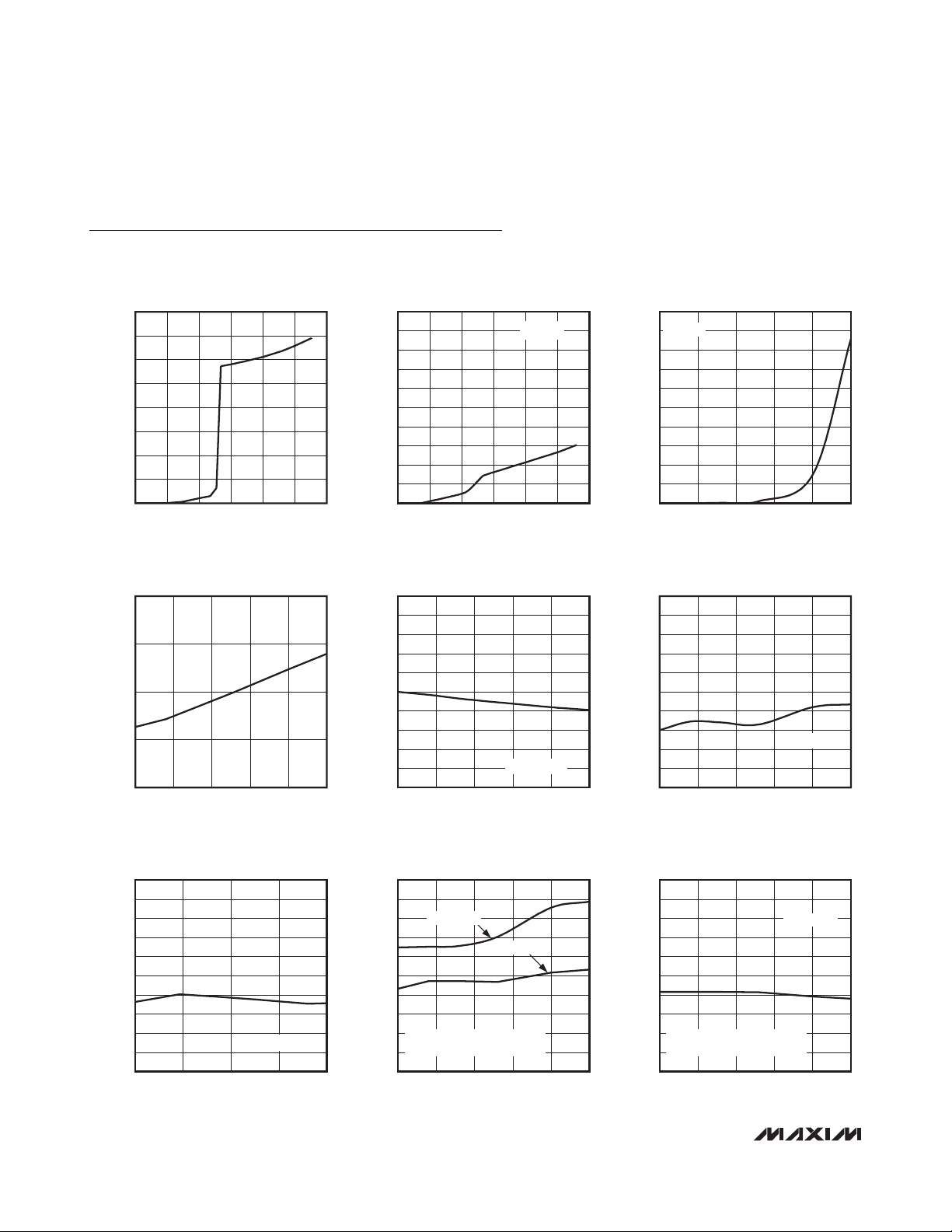
QUIESCENT SUPPLY CURRENT
vs. SUPPLY VOLTAGE
40
35
30
25
20
15
SUPPLY CURRENT (µA)
10
5
0
06
SUPPLY VOLTAGE (V)
541 2 3
MAX8586 toc01
SHUTDOWN SUPPLY CURRENT
vs. SUPPLY VOLTAGE
10
9
8
7
6
5
4
3
SUPPLY CURRRENT (µA)
2
1
0
06
SUPPLY VOLTAGE (V)
SWITCH LEAKAGE CURRENT
vs. TEMPERATURE
VON = 0V
603510-15
TEMPERATURE (°C)
VON = 0V
0.50
0.45
MAX8586 toc02
0.40
0.35
0.30
0.25
0.20
0.15
LEAKAGE CURRENT (µA)
0.10
0.05
0
54321
-40 85
MAX8586 toc03
NORMALIZED ON-RESISTANCE
vs. TEMPERATURE
1.50
1.25
ON
1.00
NORMALIZED R
0.75
0.50
-40 85
TEMPERATURE (°C)
CURRENT LIMIT
vs. INPUT VOLTAGE
2.0
1.9
1.8
1.7
1.6
1.5
1.4
CURRENT LIMIT (A)
1.3
1.2
1.1
1.0
2.7 5.5
INPUT VOLTAGE (V)
V
ENRESET
4.13.4
CONTINUOUS CURRENT LIMIT
vs. TEMPERATURE
MAX8586 toc05
CURRENT LIMIT (A)
1.50
1.48
1.46
1.44
1.42
1.40
1.38
1.36
1.34
1.32
1.30
-40 85
1.60
1.58
MAX8586 toc04
1.56
1.54
1.52
1.50
1.48
CURRENT LIMIT (A)
1.46
1.44
V
= 0V
1.42
603510-15
1.40
-40 85
TEMPERATURE (°C)
ENRESET
603510-15
SWITCH ON-TIME
vs. TEMPERATURE
9.0
8.5
MAX8586 toc07
8.0
7.5
7.0
6.5
6.0
ON-TIME (ms)
5.5
= 5V
4.8
5.0
4.5
4.0
R
= 5Ω
LOAD
NO LOAD
MEASURED FROM ON HIGH UNTIL
REACHES 90% OF THE INPUT
V
OUT
-40 85
TEMPERATURE (°C)
603510-15
10
9
MAX8586 toc08
8
7
6
5
4
3
OUTPUT FALL TIME (ms)
2
1
0
MEASURED FROM ON LOW UNTIL
V
-40 85
CURRENT LIMIT
vs. TEMPERATURE
TEMPERATURE (°C)
SWITCH OFF-TIME
vs. TEMPERATURE
FALLS TO 10% OF THE INPUT
OUT
TEMPERATURE (°C)
V
ENRESET
R
LOAD
603510-15
603510-15
= 5V
= 5Ω
MAX8586 toc06
MAX8586 toc09

MAX8586
Typical Operating Characteristics (continued)
(Typical Application Circuit, VIN= VON= V
SEL
= V
ENRESET
= 5V, TA= +25°C, unless otherwise noted.)
Single 1.2A USB Switch in
3mm x 3mm TDFN
_______________________________________________________________________________________
5
FAULT-BLANKING TIME
vs. TEMPERATURE
35
33
31
29
27
25
23
21
FAULT-BLAMKING TIME (ms)
19
17
15
-40 85
TEMPERATURE (°C)
603510-15
OVERLOAD RESPONSE INTO 2Ω
FAULT
I
IN
28
27
MAX8586 toc10
26
25
24
23
22
AUTO-RESTART CURRENT (mA)
21
20
MAX8586 toc13
AUTO-RESTART CURRENT
vs. TEMPERATURE
MAX8586 toc11
603510-15-40 85
TEMPERATURE (°C)
OVERLOAD RESPONSE INTO SHORT CIRCUIT
5V/div
2A/div
FAULT
I
IN
AUTO-RESTART CURRENT
vs. INPUT VOLTAGE
40
35
30
25
20
AUTO-RESTART CURRENT (mA)
15
R
10
2.7 5.5
INPUT VOLTAGE (V)
MAX8586 toc14
LOAD
5V/div
2A/div
= 0.5
4.84.13.4
MAX8586 toc12
Ω
I
OUT
V
OUT
V
OUT
V
ON
FAULT REMOVED
10ms/div
SWITCH TURN-ON WAVEFORM INTO NO LOAD
1ms/div
MAX8586 toc15
2A/div
5V/div
2V/div
2V/div
I
OUT
V
OUT
SWITCH TURN-ON WAVEFORM INTO 5Ω LOAD
V
OUT
V
ON
FAULT REMOVED
10ms/div
MAX8586 toc16
1ms/div
2A/div
5V/div
2V/div
2V/div

MAX8586
Single 1.2A USB Switch in
3mm x 3mm TDFN
6 _______________________________________________________________________________________
Typical Operating Characteristics (continued)
(Typical Application Circuit, VIN= VON= V
SEL
= V
ENRESET
= 5V, TA= +25°C, unless otherwise noted.)
SWITCH TURN-OFF WAVEFORM INTO 5Ω LOAD
V
OUT
V
FAULT
VIN
AC-COUPLED
I
OUT
V
OUT
ON
1ms/div
STARTUP INTO 470µF
2ms/div
MAX8586 toc17
MAX8586 toc19
2V/div
2V/div
5V/div
50mV/div
500mA/div
2V/div
FAULT
AC-COUPLED
I
OUT
V
OUT
FAULT
V
OUT
STARTUP INTO 10µF
VIN
2ms/div
UVLO RESPONSE WITH 50Ω LOAD
V
IN
4ms/div
MAX8586 toc18
5V/div
50mV/div
20mA/div
2A/div
MAX8586 toc20
5V/div
2V/div
2V/div

MAX8586
Single 1.2A USB Switch in
3mm x 3mm TDFN
_______________________________________________________________________________________ 7
Pin Description
Functional Diagram
PIN NAME FUNCTION
1 SEL
2 ISET
3ON
4IN
5 OUT
6 FAULT
ON Polarity Selector Input. Drive SEL high to select ON for an active-high enable. Drive SEL to GND to select
ON for an active-low enable.
Current-Limit Programming Input. Connect a resistor from ISET to GND to set the internal current limit. The
valid range for R
is 26kΩ to 60kΩ.
ISET
Enable Input. Drive ON high to enable the device when SEL is high. Drive ON low to enable the device when
SEL is low.
Power-Supply Input. Connect to an input power supply in the 2.75V to 5.5V range. Bypass IN to GND with a
1µF or greater ceramic capacitor.
Power Output. Bypass OUT to GND with a 1µF or greater capacitor. OUT is high impedance during
shutdown.
Open-Drain Fault-Indicator Output. FAULT is low when the input is below UVLO, or during current limit,
reverse current detection, or thermal shutdown.
7 GND Ground. Connect GND to the exposed paddle and to a ground plane.
8 ENRESET
Auto-Restart Enable Input. Drive ENRESET high to enable auto-restart mode. Drive ENRESET low to disable
auto-restart mode.
— EP Exposed Pad. Connect the exposed pad to a large ground plane to improve thermal power dissipation.
SEL
GND
IN
OSCILLATOR
CONTROL
LOGIC
CHARGE
PUMP
RESTART
CIRCUITRY
AUTO-
25mA
CURRENT-
LIMIT
CIRCUITRY
N
+
O.5V
MAX8586
20ms
TIMER
THERMALSHUTDOWN
CIRCUITRY
UVLO
ON
OUT
ISET
ENRESET
FAULT

MAX8586
Single 1.2A USB Switch in
3mm x 3mm TDFN
8 _______________________________________________________________________________________
Detailed Description
Current-Limit Protection
The MAX8586 uses two methods to protect the circuit
from overcurrent conditions. Continuous current limiting
has tighter accuracy but slower response time compared to short-circuit limiting. Combining both methods
provides a high degree of protection for a variety of
faults. When a current-limit fault occurs with V
OUT
greater than 1V, the device operates in continuous current-limit mode and limits output current to a user-programmable level. When V
OUT
is less than 1V, the
device operates in short-circuit current-limit mode and
pulses the output current to levels that are 30% (typ)
higher than the selected continuous current limit.
When either fault condition persists for 20ms (typ), the
fault flag is asserted. With the auto-restart enabled
(ENRESET high) the output also latches off and is tested with a 25mA current to detect when the fault condition has been removed. 20ms after the fault condition is
removed, the output automatically restarts. With the
auto-restart disabled (ENRESET low), the output continues to source the current-limit current as long as the
fault is present.
Reverse Current Protection
The USB specification does not allow an output device
to source current back into the USB port. However, the
MAX8586 is designed to safely power noncompliant
devices. During normal operation with the channel
enabled, if the current from the output to the input
exceeds 1A (typ) for more than 20ms (typ), the IC turns
off the switch and the FAULT flag is asserted. When the
IC is disabled, the output is switched to a high-impedance state, blocking reverse current flow from the output back to the input.
On/Off Control and UVLO
The MAX8586 has a selectable active-high/low ON
polarity. Drive SEL high to select an active-high for ON;
drive SEL low to select active-low for ON. The
MAX8586 includes a UVLO circuit to prevent erroneous
switch operation when the input voltage goes low during startup and brownout conditions. Input voltages of
less than +2.5V (typ) inhibit operation of the device.
FAULT asserts low during a UVLO condition.
Output Fault Protection and Auto-Restart
The MAX8586 uses an auto-restart function to detect
short-circuit removal by sourcing 25mA from the output
and monitoring the output voltage. When the voltage at
the output exceeds 0.5V for 20ms, the fault flag releases,
the output turns back on, and the 25mA current source
turns off. Active loads are not expected to draw measurable current when supplied with less than 0.5V. The autorestart function is enabled when ENRESET is high. Drive
ENRESET low to disable the auto-restart function. When
the auto-restart function is disabled, OUT regulates the
current to the programmed current limit.
Fault Indicator and Fault Blanking
The MAX8586 provides an open-drain output (FAULT)
to signal fault conditions. Connect FAULT to IN through
a 100kΩ pullup resistor for most applications. FAULT
asserts low when any of the following conditions occur:
• The input voltage is below the UVLO threshold.
• The switch junction temperature exceeds the
+160°C thermal-shutdown temperature limit.
• The switch is in current-limit or short-circuit currentlimit mode for longer than the fault-blanking period
(20ms typ).
• The reverse current exceeds the 1A threshold for
longer than the fault-blanking period (20ms typ).
When auto-restart is enabled, the FAULT output goes
high impedance after a 20ms delay once the fault condition is removed. With auto-restart disabled, during the
fault the output is tested every 20ms. When the fault is
removed, the FAULT output goes high impedance after
a delay that can be up to 20ms. Ensure that the
MAX8586 input bypass capacitance prevents glitches
from triggering the FAULT output. To distinguish large
capacitive loads from short circuits or sustained overloads, the MAX8586 has a fault-blanking circuit. When
a load transient causes the output to enter current limit,
an internal counter monitors the duration of the fault.
For load faults exceeding the 20ms fault-blanking time,
the switch turns off, FAULT asserts low, and the output
enters auto-restart mode (see the
Current-Limit
Protection
and
Output Fault Protection and Auto-Restart
sections). Only current-limit and short-circuit faults are
blanked. Thermal-overload faults and input voltages
below the UVLO threshold immediately turn the output
off and assert FAULT low.
Fault blanking allows the MAX8586 to handle USB
loads that might not be fully compliant with USB specifications. The MAX8586 successfully powers USB loads
with additional bypass capacitance and/or large startup currents while protecting the upstream power
source. No fault is reported if the switch brings up the
load within the 20ms blanking period.

MAX8586
Single 1.2A USB Switch in
3mm x 3mm TDFN
_______________________________________________________________________________________ 9
Thermal Shutdown
When the MAX8586 die temperature exceeds +160°C,
the switch turns off and FAULT goes low. Thermal shutdown does not utilize the 20ms fault-blanking timeout
period. When the junction temperature cools by 15°C,
the switch turns on again and FAULT returns high.
When an overload condition persists, the switch cycles
on and off, resulting in a pulsed output that reduces the
average system load.
Applications Information
Setting the Current Limit
A resistor from ISET to ground programs the currentlimit value. Use a resistor between 26kΩ and 60kΩ to
set the current limit according to the formula:
I
LIM(TYPICAL)
= 36400 / R
ISET
(Amps)
Do not use R
ISET
values below 26kΩ because the maximum current rating of the device may be exceeded.
R
ISET
values larger than 60kΩ are not recommended
and do not provide a lower limit current than 500mA. If
the output drops below 1V (typ), the MAX8586 shifts to a
short-circuit current-limit threshold that is 30% above the
programmed level given by the I
LIM(TYPICAL)
formula.
Input Power Supply and Capacitance
To limit the input voltage drop during momentary output
load transients, connect a capacitor from IN to ground.
A 1µF ceramic capacitor is required for local decoupling; however, higher capacitor values further reduce
the voltage drop at the input. When driving inductive
loads, a larger capacitance may be needed to prevent
voltage spikes from exceeding the MAX8586’s absolute
maximum ratings.
Output Capacitance
A capacitor as large as 500µF is allowed on the output
to smooth out transients and/or increase rise/fall times.
Larger output capacitance may be used, but the resulting output charge time during startup may exceed the
fault-blanking period resulting in a FAULT flag.
Driving Inductive Loads
A wide variety of devices (mice, keyboards, cameras,
and printers) typically connect to the USB port with
cables, adding an inductive component to the load. This
inductance causes the output voltage at the USB port to
oscillate during a load step. The MAX8586 drives inductive loads; however, care must be taken to avoid
exceeding the device’s absolute maximum ratings.
Usually, the load inductance is relatively small, and the
MAX8586’s input includes a substantial bulk capacitance from an upstream regulator as well as local
bypass capacitors, limiting overshoot. If severe ringing
occurs because of large load inductance, clamp the
MAX8586 output below +6V and above -0.3V.
Turn-On and Turn-Off Behavior
The MAX8586 features a slow turn-on and turn-off, minimizing loading transients on the upstream power
source. SEL sets the active polarity of the logic inputs of
the MAX8586. Drive ON to the same logic state as SEL
to enable the output. Drive ON to the opposite logic
state as SEL to disable the output (see Table 1). The
output enters a high-impedance state when disabled.
Layout and Thermal Dissipation
Keep all input/output traces as short as possible to
reduce the effect of undesirable parasitic inductance
and optimize the switch response time to output shortcircuit conditions. Place input and output capacitors no
more than 5mm from device leads. Connect IN and OUT
to the power bus with short traces. Wide power bus
planes at IN and OUT provide superior heat dissipation
as well. An active switch dissipates little power with minimal change in package temperature. Calculate the
power dissipation for this condition as follows:
P = I
OUT
2
x R
ON
At the normal operating current (I
OUT
= 0.5A) and the
maximum on-resistance of the switch (95mΩ), the
power dissipation is:
P = (0.5A)2x 0.95Ω = 24mW
The worst-case power dissipation occurs when the output current is just below the current-limit threshold with
an output voltage greater than 1V. In this case, the
power dissipated in the switch is the voltage drop
across the switch multiplied by the current limit:
P = I
LIM
x (VIN- V
OUT
)
For a 5.5V input and 1V output, the maximum power
dissipation is:
P = 1.6A x (5.5V - 1V) = 7.2W
Table 1. SEL/ON Inputs
SEL ON OUT STATE
High High Enabled
High Low Disabled
Low High Disabled
Low Low Enabled

Because the package power dissipation is 1951mW, the
MAX8586 die temperature exceeds the +160°C thermalshutdown threshold when dissipating 7.2W, and the
switch output shuts down until the junction temperature
cools by 15°C. The duty cycle and period are strong
functions of the ambient temperature and the PC board
layout (see the
Thermal Shutdown
section).
If the output current exceeds the current-limit threshold,
or the output voltage is pulled below the short-circuit
detect threshold, the MAX8586 enters a fault state after
20ms, at which point auto-restart mode is enabled and
25mA is sourced by the output to test for removal of the
overload. For a 5V input, OUT short circuited to GND,
and auto-restart mode active, the power dissipation is
as follows:
P = 0.025A x 5V = 0.125W
MAX8586
Single 1.2A USB Switch in
3mm x 3mm TDFN
10 ______________________________________________________________________________________
Chip Information
TRANSISTOR COUNT: 2117
PROCESS: BiCMOS
Figure 1. Typical Application Circuit
Pin Configuration
INPUT SUPPLY
2.75V TO 5.5V
1µF
OUTPUT
FAULT
INDICATOR
ON/OFF
POLARITY
SELECTION
CONTROL/
ON/OFF
R1
100kΩ
OUTPUT SUPPLY
C1
IN OUT
MAX8586
FAULT
SEL
ON
ENRESET
ISET
GND
UP TO 1.2A
C2
1µF
AUTO-RESTART
ON/OFF
R2
26kΩ
TOP VIEW
SEL
ISET
ON
1
2
3
4
IN
MAX8586
TDFN
8
7
6
5
ENRESET
GND
FAULT
OUT

MAX8586
Single 1.2A USB Switch in
3mm x 3mm TDFN
______________________________________________________________________________________ 11
Package Information
For the latest package outline information and land patterns, go to www.maxim-ic.com/packages. Note that a “+”, “#”, or “-” in the
package code indicates RoHS status only. Package drawings may show a different suffix character, but the drawing pertains to the
package regardless of RoHS status.
PACKAGE TYPE PACKAGE CODE DOCUMENT NO.
8 TQFN-EP T833-2
21-0137

MAX8586
Single 1.2A USB Switch in
3mm x 3mm TDFN
12 ______________________________________________________________________________________
Package Information (continued)
For the latest package outline information and land patterns, go to www.maxim-ic.com/packages. Note that a “+”, “#”, or “-” in the
package code indicates RoHS status only. Package drawings may show a different suffix character, but the drawing pertains to the
package regardless of RoHS status.
COMMON DIMENSIONS
SYMBOL
MIN. MAX.
A 0.70 0.80
D 2.90 3.10
E 2.90 3.10
0.00 0.05
A1
L0.20
0.25 MIN.k
A2 0.20 REF.
0.40
PACKAGE VARIATIONS
PKG. CODE
T633-2
T833-2
T833-3
T1033-1
T1033MK-1
T1033-2
T1433-1
T1433-2
N D2
6
1.50±0.10 2.30±0.10 0.95 BSC MO229 / WEEA 0.40±0.05 1.90 REF
8 1.50±0.10 2.30±0.10
1.50±0.10 2.30±0.10
8
10
1.50±0.10
1.50±0.10
10
10
1.70±0.10
14
14
1.70±0.10
14
E2 e
2.30±0.10
2.30±0.10
2.30±0.10
2.30±0.10
2.30±0.10
2.30±0.101.70±0.10
JEDEC SPEC
0.65 BSC
0.65 BSC
0.50 BSC
0.50 BSC MO229 / WEED-3
0.50 BSC1.50±0.10
0.40 BSC
0.40 BSC
0.40 BSC
MO229 / WEEC
MO229 / WEEC
MO229 / WEED-3
MO229 / WEED-3
- - - -
- - - -
b
[(N/2)-1] x e
0.30±0.05
0.30±0.05 1.95 REF
0.25±0.05
0.25±0.05 2.00 REF
0.25±0.05
0.20±0.05- - - -
0.20±0.05
0.20±0.05 2.40 REFT1433-3F
1.95 REF
2.00 REF
2.00 REF
2.40 REF
2.40 REF

MAX8586
Single 1.2A USB Switch in
3mm x 3mm TDFN
Maxim cannot assume responsibility for use of any circuitry other than circuitry entirely embodied in a Maxim product. No circuit patent licenses are
implied. Maxim reserves the right to change the circuitry and specifications without notice at any time.
Maxim Integrated Products, 120 San Gabriel Drive, Sunnyvale, CA 94086 408-737-7600 ____________________
13
© 2010 Maxim Integrated Products Maxim is a registered trademark of Maxim Integrated Products, Inc.
Revision History
REVISION
NUMBER
0 11/04 Initial release —
1 1/09 Added automotive part number 1
2 1/10
REVISION
DATE
DESCRIPTION
Removed UL Listing Pending note, corrected top mark for automotive part, and added
soldering temperature (reflow)
PAGES
CHANGED
1, 2
 Loading...