

Page 1
General Description
The MAX8576–MAX8579 synchronous PWM buck controllers use a hysteretic voltage-mode control algorithm
to achieve a fast transient response without requiring
loop compensation. The MAX8576/MAX8577 contain an
internal LDO regulator allowing the controllers to function from only one 3V to 28V input supply. The
MAX8578/MAX8579 do not contain the internal LDO
and require a separate supply to power the IC when the
input supply is higher than 5.5V. The MAX8576–
MAX8579 output voltages are adjustable from 0.6V to
0.9 x VINat loads up to 15A.
Nominal switching frequency is programmable over the
200kHz to 500kHz range. High-side MOSFET sensing is
used for adjustable hiccup current-limit and short-circuit protection. The MAX8576/MAX8578 can start up
into a precharged output without pulling the output voltage down. The MAX8577/MAX8579 have startup output
overvoltage protection (OVP), and will pull down a
precharged output.
Applications
Motherboard Power Supplies
AGP and PCI-Express Power Supplies
Graphic-Card Power Supplies
Set-Top Boxes
Point-of-Load Power Supplies
Features
♦ 3V to 28V Supply Voltage Range
♦ 1.2% Accurate Over Temperature
♦ Adjustable Output Voltage Down to 0.6V
♦ 200kHz to 500kHz Switching Frequency
♦ Adjustable Temperature-Compensated Hiccup
Current Limit
♦ Lossless Peak Current Sensing
♦ Monotonic Startup into Prebias Output
(MAX8576/MAX8578)
♦ Startup Overvoltage Protection
(MAX8577/MAX8579)
♦ Enable/Shutdown
♦ Adjustable Soft-Start
MAX8576–MAX8579
3V to 28V Input, Low-Cost, Hysteretic
Synchronous Step-Down Controllers
________________________________________________________________ Maxim Integrated Products 1
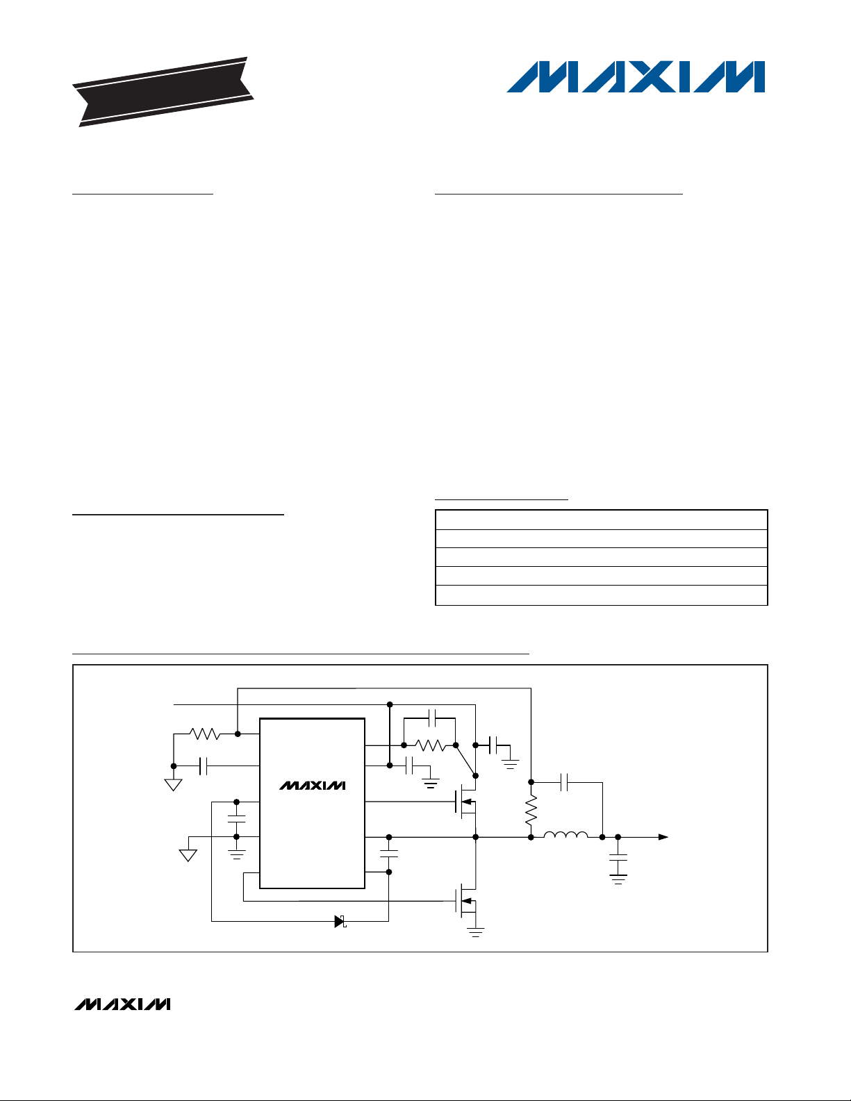
OCSET
IN
DH
LXGND
VL
SS
FB
MAX8576
MAX8577
BST
DL
INPUT
UP TO 28V
OUTPUT
0.6V TO 0.9 x V
IN
Typical Operating Circuit
19-3289; Rev 1; 6/05
For pricing, delivery, and ordering information, please contact Maxim/Dallas Direct! at
1-888-629-4642, or visit Maxim’s website at www.maxim-ic.com.
EVALUATION KIT
AVAILABLE
Ordering Information
PART
TEMP RANGE
PIN-PACKAGE
MAX8576EUB
10 µMAX
®
MAX8577EUB
10 µMAX
MAX8578EUB
10 µMAX
MAX8579EUB
10 µMAX
Pin Configurations appear at end of data sheet.
µMAX is a registered trademark of Maxim Integrated Products, Inc.
-40°C to +85°C
-40°C to +85°C
-40°C to +85°C
-40°C to +85°C
Page 2
MAX8576–MAX8579
3V to 28V Input, Low-Cost, Hysteretic
Synchronous Step-Down Controllers
2 _______________________________________________________________________________________
ABSOLUTE MAXIMUM RATINGS
Stresses beyond those listed under “Absolute Maximum Ratings” may cause permanent damage to the device. These are stress ratings only, and functional
operation of the device at these or any other conditions beyond those indicated in the operational sections of the specifications is not implied. Exposure to
absolute maximum rating conditions for extended periods may affect device reliability.
IN to GND (MAX8576/MAX8577) ...........................-0.3V to +30V
VL to GND (MAX8576/MAX8577).............................-0.3V to +6V
IN to VL (MAX8576/MAX8577) ...............................-0.3V to +30V
V
CC
to GND (MAX8578/MAX8579) ..........................-0.3V to +6V
SS to GND (MAX8576/MAX8577) ...............-0.3V to (V
VL
+ 0.3)V
SS to GND (MAX8578/MAX8579)...............-0.3V to (V
CC
+ 0.3)V
DL to GND (MAX8576/MAX8577) ...............-0.3V to (V
VL
+ 0.3)V
DL to GND (MAX8578/MAX8579) ..............-0.3V to (V
CC
+ 0.3)V
BST to GND ............................................................-0.3V to +36V
BST to LX..................................................................-0.3V to +6V
LX to GND .....................-1V (-2.5V for <50ns Transient) to +30V
DH to LX..................................................-0.3V to +(V
BST
+ 0.3)V
FB to GND ................................................................-0.3V to +6V
EN to GND (MAX8578/MAX8679EUB) .....................-0.3V to +6V
OCSET to GND (MAX8576/MAX8677) ........-0.3V to (V
IN
+ 0.3)V
OCSET to GND (MAX8578/MAX8679) ...................-0.3V to +30V
OCSET to LX (MAX8576/MAX8677) ............-0.6V to (V
IN
+ 0.3)V
OCSET to LX (MAX8578/MAX8679) .......................-0.6V to +30V
DH and DL Continuous Current ............................±250mA RMS
Continuous Power Dissipation (T
A
= +70°C)
10-Pin µMAX (derate 5.6mW/°C above +70°C) ...........444mW
Operating Temperature Range ...........................-40°C to +85°C
Junction Temperature......................................................+150°C
Storage Temperature Range .............................-65°C to +150°C
Lead Temperature (soldering, 10s) ................................+300°C
ELECTRICAL CHARACTERISTICS
(VIN= 12V (MAX8576/MAX8577 only), 4.7µF capacitor from VL (MAX8576/MAX8577 only) or VCC(MAX8578/MAX8579 only) to GND;
V
CC
= VEN= 5V (MAX8578/MAX8579 only); 0.01µF capacitor from SS to GND; VFB= 0.65V; V
BST
= 5V; VLX= V
GND
= 0V; V
OCSET
=
11.5V; DH = unconnected; DL = unconnected; T
A
= 0°C to +85°C, unless otherwise noted. Typical values are at TA= +25°C.)
PARAMETER CONDITIONS
UNITS
SUPPLY VOLTAGES
MAX8576/MAX8577 5.5
IN Supply Voltage
IN = VL (MAX8576/MAX8577) 3.0 5.5
V
VCC Input Voltage MAX8576/MAX8577 3.0 5.5 V
VL Output Voltage IVL = 10mA (MAX8576/MAX8577)
5.0
V
VL Maximum Output Current MAX8576/MAX8577 20 mA
Rising
2.8
Falling 2.4
2.5
V
VL or VCC Undervoltage Lockout
(UVLO)
Hysteresis
mV
VIN = 12V 0.6 2
VIN = VVL = 5V 1.1 3
No switching, VFB = 0.65V
(MAX8576/MAX8577)
V
IN
= VVL = 3.3V 0.6 2
V
CC
= 5V 0.6 2
Supply Current
V
EN
= 0V or VFB = 0.65V, no
switching (MAX8578/MAX8579)
V
CC
= 3.3V 0.6 2
mA
REGULATOR
Output Regulation Accuracy VFB peak
0.6
V
Output Regulation Hysteresis (Note 1)
20
mV
FB falling to DL falling 50
FB Propagation Delay
FB rising to DH falling 70
ns
Overvoltage-Protection (OVP)
Threshold
V
TA = +85°C60
High-Side Current-Sense
Program Current (Note 2)
T
A
= +25°C
50
µA
MIN TYP MAX
4.75
2.75
2.45
350
0.593
12.5
0.70 0.75 0.80
42.5
28.0
5.25
2.90
0.607
28.0
57.5
Page 3
MAX8576–MAX8579
3V to 28V Input, Low-Cost, Hysteretic
Synchronous Step-Down Controllers
_______________________________________________________________________________________ 3
ELECTRICAL CHARACTERISTICS (continued)
(VIN= 12V (MAX8576/MAX8577 only), 4.7µF capacitor from VL (MAX8576/MAX8577 only) or VCC(MAX8578/MAX8579 only) to GND;
V
CC
= VEN= 5V (MAX8578/MAX8579 only); 0.01µF capacitor from SS to GND; VFB= 0.65V; V
BST
= 5V; VLX= V
GND
= 0V; V
OCSET
=
11.5V; DH = unconnected; DL = unconnected; T
A
= 0°C to +85°C, unless otherwise noted. Typical values are at TA= +25°C.)
PARAMETER CONDITIONS
UNITS
High-Side Current-Sense
Overcurrent Trip Adjustment
Range
V
IN
- V
OCSET
V
Soft-Start Internal Resistance 45 80 125 kΩ
Fault Hiccup Internal SS Pulldown
Current
V
LX
< V
OCSET
and VFB < V
SS
nA
DRIVER SPECIFICATIONS
Sourcing current 2.6 4.0
DH Driver Resistance
Sinking current 1.9 3.0
Ω
Sourcing current 2.6 4.0
DL Driver Resistance
Sinking current 1.1 2.0
Ω
Dead Time
DH low to DL high and DL low to DH high
(adaptive)
40 ns
DH Minimum On-Time
245 ns
Normal operation
220
DL Minimum On-Time
Current fault
ns
BST Current V
BST
- VLX = 5.5V, VLX = 28V, VFB < V
SS
mA
EN
Input Voltage Low VCC = 3V (MAX8578/MAX8579) 0.7 V
Input Voltage High VCC = 5.5V (MAX8578/MAX8579) 1.5 V
THERMAL SHUTDOWN
Thermal Shutdown Rising temperature, hysteresis = 20°C (typ)
°C
ELECTRICAL CHARACTERISTICS
(VIN= 12V (MAX8576/MAX8577 only), 4.7µF capacitor from VL (MAX8576/MAX8577 only) or VCC(MAX8578/MAX8579 only) to GND;
V
CC
= VEN= 5V (MAX8578/MAX8579 only); 0.01µF capacitor from SS to GND; VFB= 0.65V; V
BST
= 5V; VLX= V
GND
= 0V; V
OCSET
=
11.5V; DH = unconnected; DL = unconnected; T
A
= -40°C to +85°C, unless otherwise noted. Note 3)
PARAMETER CONDITIONS
UNITS
SUPPLY VOLTAGES
MAX8576/MAX8577 5.5
IN Supply Voltage
IN = VL, MAX8576/MAX8577 3.0 5.5
V
VCC Input Voltage MAX8576/MAX8577 3.0 5.5 V
VL Output Voltage IVL = 10mA, MAX8576/MAX8577
V
VL Maximum Output Current MAX8576/MAX8577 20 mA
MIN TYP MAX
0.05 0.40
250
140
120
580
1.65
+160
MIN TYP MAX
4.75 5.25
28.0
Page 4

MAX8576–MAX8579
3V to 28V Input, Low-Cost, Hysteretic
Synchronous Step-Down Controllers
4 _______________________________________________________________________________________
Note 1: Guaranteed by design.
Note 2: This current linearly compensates for the MOSFET temperature coefficient.
Note 3: Specifications to -40
°C are guaranteed by design and not production tested.
ELECTRICAL CHARACTERISTICS (continued)
(VIN= 12V (MAX8576/MAX8577 only), 4.7µF capacitor from VL (MAX8576/MAX8577 only) or VCC(MAX8578/MAX8579 only) to GND;
V
CC
= VEN= 5V (MAX8578/MAX8579 only); 0.01µF capacitor from SS to GND; VFB= 0.65V; V
BST
= 5V; VLX= V
GND
= 0V; V
OCSET
=
11.5V; DH = unconnected; DL = unconnected; T
A
= -40°C to +85°C, unless otherwise noted. Note 3)
PARAMETER CONDITIONS
UNITS
Rising
VL or VCC Undervoltage Lockout
(UVLO)
Falling
V
VIN = 12V 2
VIN = VVL = 5V 3.5
No switching, VFB = 0.65V
(MAX8576/MAX8577)
V
IN
= VVL = 3.3V 2
V
CC
= 5V 2
Supply Current
V
EN
= 0V or VFB = 0.65V, no
switching (MAX8578/MAX8579)
V
CC
= 3.3V 2
mA
REGULATOR
Output Regulation Accuracy VFB peak
V
Overvoltage-Protection (OVP)
Threshold
V
High-Side Current-Sense OverCurrent Trip Adjustment Range
V
IN
- V
OCSET
V
DRIVER SPECIFICATIONS
Sourcing current 4
DH Driver Resistance
Sinking current 3.0
Ω
Sourcing current 4.0
DL Driver Resistance
Sinking current 2.0
Ω
DH Minimum On-Time
ns
DL Minimum On-Time Normal operation
ns
EN
Input Voltage Low VCC = 3V, MAX8578/MAX8579 0.7 V
Input Voltage High VCC = 5.5V, MAX8578/MAX8579 1.5 V
MIN TYP MAX
2.75 2.90
2.40 2.55
0.591 0.607
0.70 0.80
0.05 0.40
245
220
Page 5
MAX8576–MAX8579
3V to 28V Input, Low-Cost, Hysteretic
Synchronous Step-Down Controllers
_______________________________________________________________________________________ 5
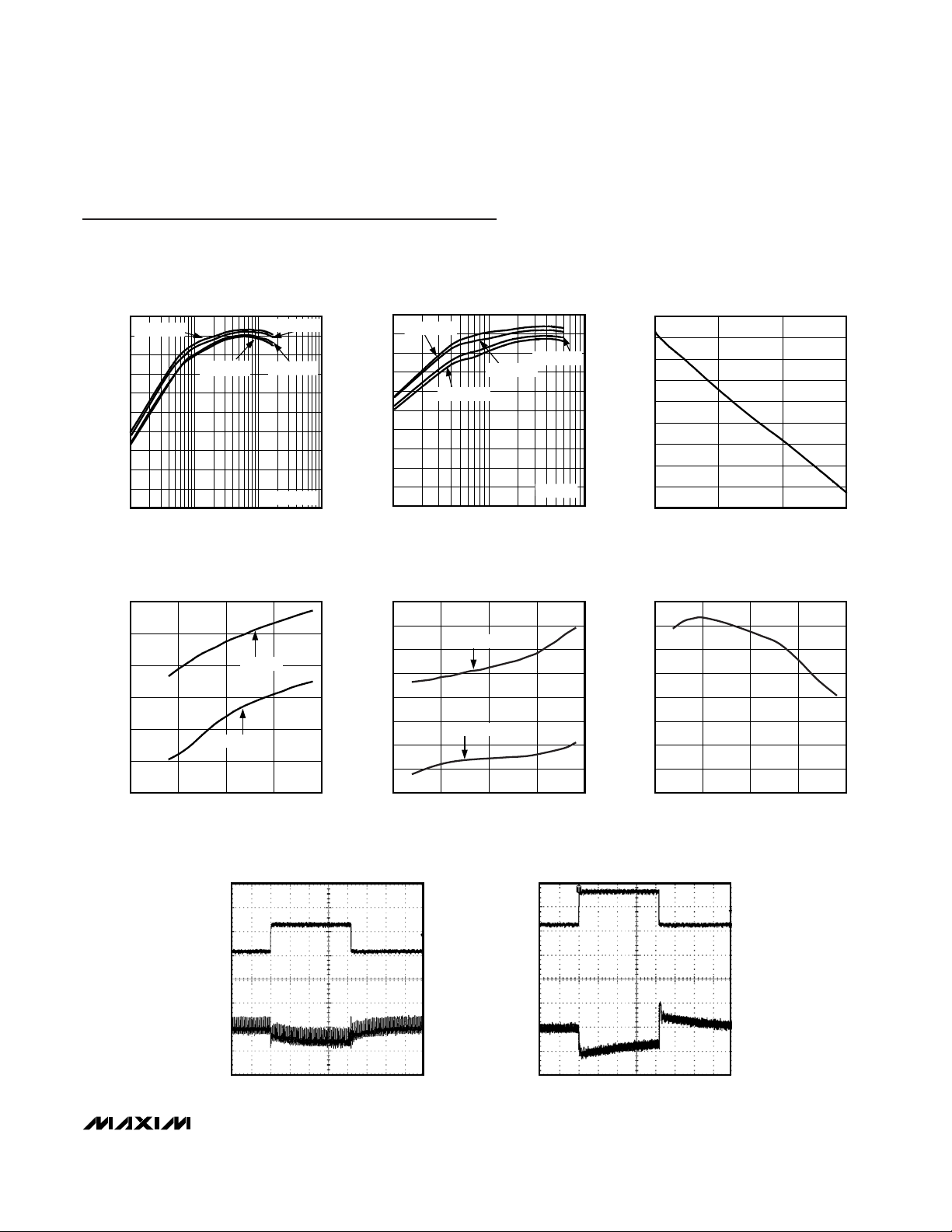
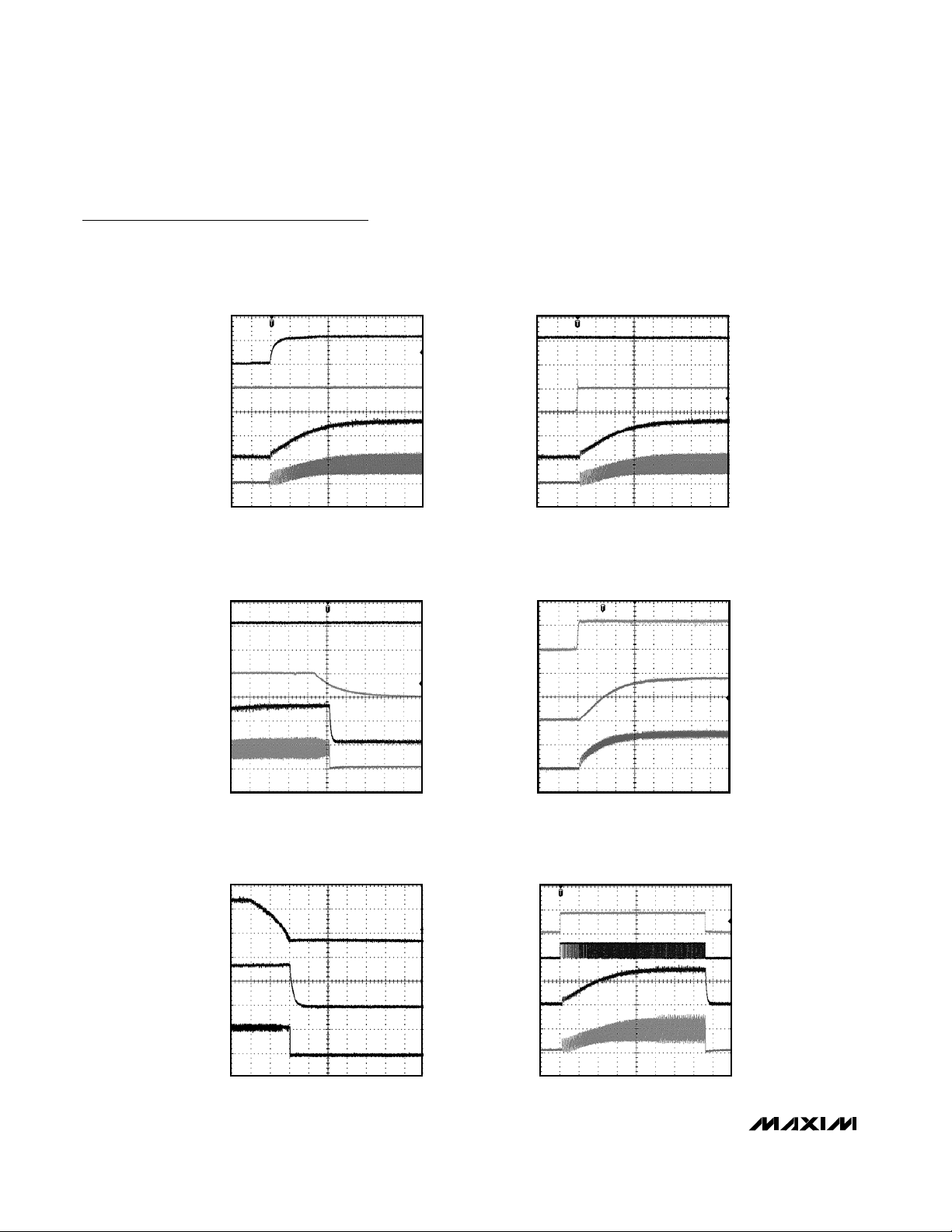
EFFICIENCY vs. LOAD CURRENT
(CIRCUIT OF FIGURE 2)
MAX8576-79 toc01
LOAD CURRENT (A)
EFFICIENCY (%)
101
10
20
30
40
50
60
70
80
90
100
0
0.1 100
V
OUT
= 3.3V
V
OUT
= 2.5V
V
OUT
= 1.8V
V
OUT
= 1.5V
VIN = 12V
EFFICIENCY vs. LOAD CURRENT
(CIRCUIT OF FIGURE 3)
MAX8576-79 toc02
LOAD CURRENT (A)
EFFICIENCY (%)
1
10
20
30
40
50
60
70
80
90
100
0
0.1 10
V
OUT
= 3.3V
V
OUT
= 2.5V
V
OUT
= 1.8V
V
OUT
= 1.5V
VIN = 12V
LOAD REGULATION
(CIRCUIT OF FIGURE 2)
MAX8576-79 toc03
LOAD CURRENT (A)
OUTPUT VOLTAGE (V)
105
1.76
1.77
1.78
1.79
1.80
1.81
1.82
1.83
1.84
1.75
015
LINE REGULATION
(CIRCUIT OF FIGURE 2)
MAX8576-79 toc04
INPUT VOLTAGE (V)
OUTPUT VOLTAGE (V)
201510
1.80
1.81
1.82
1.83
1.84
1.85
1.79
525
0A LOAD
15A LOAD
LINE REGULATION
(CIRCUIT OF FIGURE 3)
MAX8576-79 toc05
INPUT VOLTAGE (V)
OUTPUT VOLTAGE (V)
201510
1.72
1.74
1.78
1.80
1.82
1.84
1.86
1.70
525
NO LOAD
5A LOAD
1.76
SWITCHING FREQUENCY vs. INPUT
VOLTAGE (CIRCUIT OF FIGURE 3)
MAX8576-79 toc06
INPUT VOLTAGE (V)
SWITCHING FREQUENCY (kHz)
201510
250
300
350
400
500
550
600
200
525
450
LOAD TRANSIENT
(CIRCUIT OF FIGURE 2)
MAX8576-79 toc07
40μs/div
I
OUT
V
OUT
50mV/div
AC-COUPLED
6A
12A
LOAD TRANSIENT
(CIRCUIT OF FIGURE 3)
MAX8576-79 toc08
40μs/div
I
OUT
V
OUT
50mV/div
AC-COUPLED
5A
2.5A
Typical Operating Characteristics
(TA= +25°C, unless otherwise noted.)
Page 6
MAX8576–MAX8579
3V to 28V Input, Low-Cost, Hysteretic
Synchronous Step-Down Controllers
6 _______________________________________________________________________________________
Typical Operating Characteristics (continued)
( TA= +25°C, unless otherwise noted.)
POWER-DOWN
(CIRCUIT OF FIGURE 2, MAX8576)
MAX8576-79 toc13
4ms/div
V
IN
V
OUT
I
LX
5V/div
0
1V/div
0
0
10A/div
STARTUP AND SHUTDOWN
(CIRCUIT OF FIGURE 3)
MAX8576-79 toc14
400μs/div
V
EN
V
DL
V
OUT
I
LX
2V/div
0
10V/div
1V/div
0
0
5A/div
0
POWER-DOWN V
CC
(CIRCUIT OF FIGURE 3)
MAX8576-79 toc11
400μs/div
V
IN
V
CC
V
OUT
I
LX
10V/div
0
5V/div
1V/div
5A/div
0
POWER-UP
(CIRCUIT OF FIGURE 2)
MAX8576-79 toc12
1ms/div
V
IN
V
OUT
I
LX
10V/div
0
1V/div
0
0
10A/div
POWER-UP V
IN
(CIRCUIT OF FIGURE 3)
MAX8576-79 toc09
400μs/div
V
IN
V
CC
V
OUT
I
LX
10V/div
0
5V/div
1V/div
5A/div
0
POWER-UP V
CC
(CIRCUIT OF FIGURE 3)
MAX8576-79 toc10
400μs/div
V
IN
V
CC
V
OUT
I
LX
10V/div
0
5V/div
1V/div
5A/div
0
Page 7

MAX8576–MAX8579
3V to 28V Input, Low-Cost, Hysteretic
Synchronous Step-Down Controllers
_______________________________________________________________________________________ 7
Typical Operating Characteristics (continued)
( TA= +25°C, unless otherwise noted.)
OUTPUT OVERVOLTAGE PROTECTION
(CIRCUIT OF FIGURE 2)
MAX8576-79 toc19
200μs/div
V
DH
V
OUT
V
DL
V
FB
20V/div
5V/div
0
0.5V/div
0
1V/div
0
0
NONMONOTONIC OUTPUT-VOLTAGE RISE
(CIRCUIT OF FIGURE 2, MAX8577)
MAX8576-79 toc17
1ms/div
V
IN
V
LX
V
OUT
V
DL
10V/div
1.5V
0.5V/div
20V/div
5V/div
0
SHORT CIRCUIT AND RECOVERY
(CIRCUIT OF FIGURE 2)
MAX8576-79 toc18
10ms/div
V
IN
I
OUT
I
IN
V
OUT
10V/div
2A/div
10A/div
2V/div
0
STARTUP AND SHUTDOWN
(CIRCUIT OF FIGURE 2)
MAX8576-79 toc15
4ms/div
V
GS(Q3)
V
SS
V
OUT
I
LX
10V/div
0
0
0.5V/div
2V/div
0
0
10A/div
MONOTONIC OUTPUT-VOLTAGE RISE
(CIRCUIT OF FIGURE 2, MAX8576)
MAX8576-79 toc16
1ms/div
V
IN
V
LX
V
OUT
V
DL
10V/div
1.5V
0.5V/div
20V/div
5V/div
0
Page 8

MAX8576–MAX8579
3V to 28V Input, Low-Cost, Hysteretic
Synchronous Step-Down Controllers
8 _______________________________________________________________________________________
PIN
NAME
FUNCTION
11FB
Feedback Input. Regulates at V
FB
= 0.59V. Connect FB to a resistor-divider to set the output
voltage. See the Setting the Output Voltage section.
22S S
S oft- S tar t. U se an exter nal cap aci tor ( C
SS
) to ad j ust the soft- star t ti m e. An i nter nal 80kΩ r esi stor g i ves
ap p r oxi m atel y 4m s soft- star t ti m e for a 0.01µF exter nal cap aci tor . An i nter nal 250nA cur r ent si nk i n
hi ccup m od e g i ves ap p r oxi m atel y 10% d uty cycl e d ur i ng faul t cond i ti ons.
3—VL
Internal 5V Linear-Regulator Output. Bypass with a 4.7µF or larger ceramic capacitor. Must be
connected to IN for operation from a 3.3V to 5.5V input.
—3VCCSupply Input (3V to 5.5V). Bypass with a 4.7µF or larger ceramic capacitor to GND.
4 4 GND Ground
5 5 DL Low-Side Gate-Drive Output. Drives the synchronous-rectifier MOSFET.
6 6 BST
Boost-Capacitor Connection for High-Side Gate-Drive Output. Connect a 0.1µF ceramic
capacitor from BST to LX and a Schottky or switching diode and a 4.7Ω series resistor from
BST to VL (MAX8576/MAX8577) or V
CC
(MAX8578/MAX8579). See Figure 4.
7 7 LX External Inductor Connection. Connect LX to the junctions of the MOSFETs and inductor.
8 8 DH High-Side Gate-Drive Output. Drives the high-side MOSFET.
9—IN
Supply Voltage Input of the Internal Linear Regulator (3V to 28V). Connect to VL for operation
from 3V to 5.5V input. Connect a 0.47µF or larger ceramic capacitor from IN to GND.
—9EN
Enable Input. A logic low on EN shuts down the converter and discharges the soft-start
capacitor. Drive high or connect to V
CC
for normal operation.
10 10
Overcurrent-Limit Set. Programs the high-side peak current-limit threshold by setting the
maximum-allowed V
DS
voltage drop across the high-side MOSFET. Connect a resistor from IN
to OCSET; an internal 50µA current sink sets the maximum voltage drop relative to V
IN
. See the
Setting the Current Limit section.
Pin Description
MAX8576/
MAX8577
MAX8578/
MAX8579
OCSET
Page 9

MAX8576–MAX8579
3V to 28V Input, Low-Cost, Hysteretic
Synchronous Step-Down Controllers
_______________________________________________________________________________________ 9
Figure 1. Functional Diagram
0.3
0.75V
0.05V
OVP
LX
FAULT
SS
V
CC
VL
REFOK
VLOK
GND
IN
FB
OCSET
MAX8578/
MAX8579
EN
SS
RAMP
LOGIC
DRIVERS
GND
VL REG
POK
REF
DHI
DLI
MAX8576–MAX8579
BST
DH
LX
DL
MAX8578
MAX8579
MAX8576
MAX8577
Page 10

MAX8576–MAX8579
3V to 28V Input, Low-Cost, Hysteretic
Synchronous Step-Down Controllers
10 ______________________________________________________________________________________
Figure 2. MAX8576/MAX8577 Typical Application Circuit
Q2
R2
1
2
3
4
5
10
9
8
7
6
OCSET
IN
DH
LXGND
VL
SS
FB
MAX8576
MAX8577
BSTDL
INPUT
9V TO 24V
Q3
12V INPUT, 1.8V/12A OUTPUT (f
S
= 300kHz)
CIRCUIT IS TARGETED FOR 10.8V TO 13.2V INPUT. HOWEVER, INPUT RANGE OF 9V TO 24V
IS POSSIBLE FOR IC EVALUATION. 30V RATED MOSFET MUST BE INSTALLED IF INPUT IS
RAISED ABOVE 16V. ALL OTHER COMPONENTS CAN REMAIN UNCHANGED.
R1
D1
C6
C4
C7
R3
C13
R6
C11
C5
L1
OUTPUT
1.8V/12A
C3
Q1
C1
C2
C8
C12
C9
C10
R4
R5
ON
OFF
R7
R8
Figure 3. MAX8578/MAX8579 Typical Application Circuit
Q5
R10
1
2
3
4
5
10
9
8
7
6
OCSET
EN
DH
LXGND
V
CC
SS
FB
MAX8578
MAX8579
BSTDL
12V INPUT, 1.8V/5A OUTPUT (f
S
= 500kHz, ALL CERAMIC)
CIRCUIT IS TARGETED FOR 10.8V TO 13.2V INPUT. HOWEVER, INPUT RANGE OF 9V TO 24V
IS POSSIBLE FOR IC EVALUATION. 30V RATED MOSFET MUST BE INSTALLED IF INPUT IS
RAISED ABOVE 16V. ALL OTHER COMPONENTS CAN REMAIN UNCHANGED.
R9
D2
C17
C16
C18
R11
C23
R12
C21
L2
V
OUT
1.8V/5A
Q4
C15
C14
C19
C20 C22
ON
OFF
R13
INPUT
9V TO 24V
3V TO 5.5V
Page 11
MAX8576–MAX8579
3V to 28V Input, Low-Cost, Hysteretic
Synchronous Step-Down Controllers
______________________________________________________________________________________ 11
Detailed Description
The MAX8576–MAX8579 synchronous PWM buck controllers use Maxim’s proprietary hysteretic voltagemode control algorithm to achieve fast transient
response without any loop-compensation requirement.
The controller drives a pair of external n-channel power
MOSFETs to improve efficiency and cost. The
MAX8576/MAX8577 contain an internal linear lowdropout (LDO) regulator allowing the controller to operate from a single 3V to 28V input supply. The
MAX8578/MAX8579 do not contain the internal LDO
and require a separate supply to power the IC when the
input supply is higher than 5.5V. The MAX8576–
MAX8579 output voltages are adjustable from 0.6V to
0.9 x VINat loads up to 15A.
MAX8576/MAX8577
External Component List
COMPONENTS
QTY
DESCRIPTION/VENDOR PART
NUMBER
C1, C2
470µF, 35V aluminum electrolytic
capacitors
Sanyo 35MV470WX
C3
10µF, 25V X7R ceramic capacitor
C4
0.01µF, 10V X7R ceramic capacitor
C5
1µF, 35V X7R ceramic capacitor
C6
4.7µF, 6.3V X5R ceramic capacitor
C7, C12
0.1µF, 10V X7R ceramic capacitors
C8
0.027µF, 25V X7R ceramic capacitor
C9, C10
2200µF, 6.3V aluminum electrolytic
capacitors
Rubycon 6.3MBZ2200M10X20
C11
0.01µF, 25V X5R ceramic capacitor
C13
3300pF, 6.3V X5R ceramic capacitor
D1
High-speed diode, 100V, 250mA
Philips BAS316 (SOD-323)
L1
1.8µH, 14A, 3.48mΩ
Panasonic ETQP2H1R8BFA
Q1
30V, 12.5mΩ (max), SO-8
International Rectifier IRF7821
Q2
30V, 3.7mΩ, SO-8
International Rectifier IRF7832
Q3
2N7002 SOT-23
R1
6.04kΩ ±1% resistor
R2
5.11 kΩ ±1% resistor
R3
12.4kΩ ±1% resistor
R4
1kΩ ±5% resistor
R5
20kΩ ±5% resistor
R6
2Ω ±5% resistor
R7
10Ω ±5% resistor
R8
4.7Ω ±5% resistor
MAX8578/MAX8579
External Component List
COMPONENT
QTY
DESCRIPTION/VENDOR PART
NUMBER
C14
10µF, 25V X5R ceramic capacitor
C15
1µF, 25V X5R ceramic capacitor
C16
4700pF, 10V X7R ceramic capacitor
C17
4.7µF, 6.3V X5R ceramic capacitor
C18
0.1µF, 10V X7R ceramic capacitor
C19
0.01µF, 25V X7R ceramic capacitor
C20
47µF, 6.3V, ESR = 5mΩ, ceramic
capacitor
Taiyo Yuden JMK432476MM
C21
0.01µF, 25V X5R ceramic capacitor
C22
Optional (47µF, 6.3V, ESR = 5mΩ
ceramic capacitor
Taiyo Yuden JMK432476MM)
C23
1000pF, 25V X5R ceramic capacitor
D2
High-speed diode, 100V, 250mA
Philips BAS316 (SOD-323)
L2
2.2µH, 7.3A, 9.8mΩ
Sumida CDEP104L-2R2
Q4
30V, 18mΩ (max), SO-8
International Rectifier IRF7807Z
Q5
30V, 9.5mΩ, SO-8
International Rectifier IRF7821
R9
6.04kΩ ±1% resistor
R10
2.49kΩ ±1% resistor
R11
12.4kΩ ±1% resistor
R12
2Ω ±5% resistor
R13
4.7Ω ±5% resistor
2
1
1
1
1
2
1
2
1
1
1
1
1
1
1
1
1
1
1
1
1
1
1
1
1
1
1
1
1
1
1
0
1
1
1
1
1
1
1
1
1
1
Page 12

MAX8576–MAX8579
3V to 28V Input, Low-Cost, Hysteretic
Synchronous Step-Down Controllers
12 ______________________________________________________________________________________
Nominal switching frequency is programmable over the
200kHz to 500kHz range. High-side MOSFET sensing
is used for adjustable hiccup current-limit and short-circuit protection. The MAX8576/MAX8578 can start up
into a precharged output without pulling the output voltage down. The MAX8577/MAX8579 have startup output
overvoltage protection (OVP).
The MAX8578/MAX8579 have a logic-enable input to
turn on and off the output. The MAX8576/MAX8577 are
turned off by pulling SS low with an external small
n-channel MOSFET (see Figure 2).
DC-DC Converter Control Architecture
A proprietary hysteretic-PWM control scheme ensures
high efficiency, fast switching, and fast transient
response. This control scheme is simple: when the output voltage falls below the regulation threshold, the
error comparator begins a switching cycle by turning
on the high-side switch. This switch remains on until the
minimum on-time expires and the output voltage is in
regulation or the current-limit threshold is exceeded.
Once off, the high-side switch remains off until the minimum off-time expires and the output voltage falls below
the regulation threshold. During this period, the lowside synchronous rectifier turns on and remains on until
the voltage at FB drops below its regulation threshold.
The internal synchronous rectifier eliminates the need
for an external Schottky diode.
Voltage-Positioning Load Regulation
As seen in Figures 2 and 3, the MAX8576–MAX8579 use
a unique feedback network. By taking feedback from the
LX node through R3 (R11 for the MAX8578/MAX8579),
the usual phase lag due to the output capacitor does not
exist, making the loop stable for either electrolytic or
ceramic output capacitors. This configuration causes the
output voltage to shift by the inductor DC resistance multiplied by the load current. This voltage-positioning load
regulation greatly reduces overshoot during load transients, which effectively halves the peak-to-peak outputvoltage excursions compared to traditional step-down
converters. See the Load Transient graphs in the Typical
Operating Characteristics.
Internal 5V Linear Regulator
All MAX8576/MAX8577 functions are powered from the
on-chip, low-dropout 5V regulator with the input connected to IN. Bypass the regulator’s output (VL) with a
1µF or greater ceramic capacitor. The capacitor must
have an equivalent series resistance (ESR) of no
greater than 10mΩ. When VINis less than 5.5V, short
VL to IN. The MAX8578/MAX8579 do not have the onchip 5V regulator and must use a separate external
supply from 3V to 5.5V connected to VCCif the input
voltage is greater than 5.5V.
Undervoltage Lockout
If VL (MAX8576/MAX8577) or VCC(MAX8578/MAX8579)
drops below 2.45V (typ), the MAX8576–MAX8579
assume that the supply voltage is too low for proper circuit operation, so the UVLO circuitry inhibits switching
and forces the DL and DH gate drivers low for the
MAX8576/MAX8578, and DH low and DL high for the
MAX8577/MAX8579. After VINrises above 2.8V (typ),
the controller goes into the startup sequence and
resumes normal operation.
Output Overvoltage Protection
The MAX8576–MAX8579 output overvoltage protection
is provided by a glitch-resistant comparator on FB with
a trip threshold of 750mV (typ). The overvoltage-protection circuit is latched by an OVP fault, terminating the
run cycle and setting DH low and DL high. The fault is
cleared by toggling EN or UVLO. Output OVP is active
whenever the internal reference is in regulation.
Startup and Soft-Start
The soft-start sequence is initiated upon initial powerup, recovering from UVLO, or driving EN (MAX8578/
MAX8579) high from a low state, or releasing SS
(MAX8576/MAX8577) from a low state. The external
soft-start capacitor (CSS) is connected to an internal
resistor-divider that exponentially charges the capacitor
to 0.6V, with an SS ramp interval of 5 x RC or 4ms per
0.01µF. SS is one input to the internal voltage error
comparator, while FB is the other input. The output voltage fed back to FB tracks the rising SS voltage.
Switching commences immediately if VFBis initially less
than VSS; if VFBis greater than VSS, DH remains low
until VFBis less than VSS. DL remains low in the
MAX8576/MAX8578. This prevents the converter from
operating in reverse. However, DL is high before startup in the MAX8577/MAX8579 to enable OVP protection
in case the high-side MOSFET is shorted.
Enable
Connecting EN to GND or logic low places the
MAX8578/MAX8579 in shutdown mode. In shutdown,
DH and DL are forced low, and the voltage at SS is discharged with a 250nA current, resulting in a ramp-down
interval of approximately 10x the soft-start ramp-up
interval. V
SS
must fall to within 50mV of GND before
another cycle can commence. SS (MAX8576/
MAX8577) or EN (MAX8578/MAX8579) do not need to
be cycled after an overcurrent event. Connect EN to
VCCor logic high for normal operation. To shut down the
MAX8576/MAX8577, use an external circuit connected
Page 13

MAX8576–MAX8579
3V to 28V Input, Low-Cost, Hysteretic
Synchronous Step-Down Controllers
______________________________________________________________________________________ 13
to SS. See Figure 2 for details. The maximum on-resistance of the small external n-channel MOSFET should
be less than 40Ω so that the SS voltage is below 10mV.
Synchronous-Rectifier Driver (DL)
Synchronous rectification reduces conduction losses in
the rectifier by replacing the normal Schottky catch
diode with a low-resistance MOSFET switch. The
MAX8576–MAX8579 also use the synchronous rectifier
to ensure proper startup of the boost gate-driver circuit.
The DL low-side waveform is always the complement of
the DH high-side drive waveform (with controlled dead
time to prevent cross-conduction or shoot-through). A
dead-time circuit monitors the DL output and prevents
the high-side MOSFET from turning on until DL is fully
off. For the dead-time circuit to work properly, there
must be a low-resistance, low-inductance path from the
DL driver to the MOSFET gate. Otherwise, the sense
circuitry in the MAX8576–MAX8579 may interpret the
MOSFET gate as off when gate charge actually
remains. Use very short, wide traces (50 mils to 100
mils wide if the MOSFET is 1in from the device). The
dead time at the other edge (DH turning off) is also
determined through gate sensing.
High-Side Gate-Drive Supply (BST)
Gate-drive voltage for the high-side n-channel switch is
generated by a flying-capacitor boost circuit (Figure 4).
The capacitor between BST and LX is charged from the
IN supply up to VINminus the diode drop while the lowside MOSFET is on. When the low-side MOSFET is
switched off, the stored voltage of the capacitor is
stacked above LX to provide the necessary turn-on
voltage (VGS) for the high-side MOSFET. The controller
then closes an internal switch between BST and DH to
turn the high-side MOSFET on.
Current-Limit Circuit
Current limit is set externally with a resistor from OCSET
to the drain of the high-side n-channel MOSFET that is
normally connected to the input supply. The resistor
programs the high-side peak current limit by setting the
maximum-allowed V
DS(ON)
voltage drop across the
high-side MOSFET. An internal 50µA current sink sets
the maximum voltage drop relative to VIN. If V
FB
<
300mV, any overcurrent event (VDSof the high-side
n-channel MOSFET is larger than the limit programmed
at OCSET) immediately sets DH low and terminates the
run cycle. If V
FB
> 300mV and an overcurrent event is
detected, DH is immediately set low and four sequential
overcurrent events terminate the run cycle. Once the
run cycle is terminated, the SS capacitor is slowly discharged through the internal 250nA current sink to provide a hiccup current-limit effect. Choosing the proper
value resistor is discussed in the Setting the Current
Limit section.
Switching Frequency
Nominal switching frequency is programmable over the
200kHz to 500kHz range. This allows tradeoffs in efficiency, switching frequency, inductor value, and component size. Faster switching frequency allows for
smaller inductor values but does result in some efficiency loss. Inductor-value calculations are provided in the
Inductor Value section. The switching frequency is
tuned by the selection of the feed-forward capacitor
(CFF). See the Feed-Forward Capacitor section.
Thermal-Overload Protection
Thermal-overload protection limits total power dissipation in the MAX8576–MAX8579. When the junction temperature exceeds TJ= +160°C, an internal thermal
sensor shuts down the IC, allowing the IC to cool. The
thermal sensor turns the IC on again after the junction
temperature cools to +140°C, resulting in a pulsed output during continuous thermal-overload conditions.
Design Procedures
Setting the Output Voltage
Select an output voltage between 0.6V and 0.9 x VINby
connecting FB to a resistive voltage-divider between LX
and GND (see Figures 2 and 3). Choose R1 for approximately 50µA to 150µA bias current in the resistive
divider. A wide range of resistor values is acceptable,
but a good starting point is to choose R1 as 6.04kΩ.
Then, R3 is given by:
Figure 4. DH Boost Circuit
MAX8576–
MAX8579
BST
IN
DH
DL
LX
N
N
Page 14

MAX8576–MAX8579
3V to 28V Input, Low-Cost, Hysteretic
Synchronous Step-Down Controllers
14 ______________________________________________________________________________________
where VFB= 0.590V, RDCis the DC resistance of the
output inductor, I
OUTMAX
is the maximum output current. The term 0.01V is to reflect 1/2 of the feedbackthreshold hysteresis.
Inductor Value
The inductor value is bounded by two operating parameters: the switching frequency and the inductor peakto-peak ripple current. The peak-to-peak ripple current
is typically in the range of 20% to 40% of the maximum
output current. The equation below defines the inductance value:
where LIR is the ratio of inductor current ripple to DC
load current and fSis the switching frequency. A good
compromise between size, efficiency, and cost is an
LIR of 30%. The selected inductor must have a saturated current rating above the sum of the maximum output
current and half of the peak-to-peak ripple current. The
DC current rating of the inductor must be above the
maximum output current to keep the temperature rise
within the desired range. In addition, the DC resistance
of the inductor must meet the requirement below:
where ΔV
OUT
is the maximum-allowed output-voltage
drop from no load to full load (I
OUTMAX
).
Setting the Current Limit
Resistor R2 (R7 for the MAX8577/MAX8579) of Figure 2
(Figure 3 for the MAX8577/MAX8579) sets the current
limit and is connected between OCSET and the drain of
the high-side n-channel MOSFET. An internal 50µA
current sink sets the maximum voltage drop across the
high-side n-channel MOSFET relative to VIN. The maximum VDSdrop needs to be determined. This is calculated by:
I
DS(MAX)
must be equal or greater than the maximum
peak inductor current at the maximum output current.
Use R
DS(ON)MAX
at the junction temperature of +25°C.
The current limit is temperature compensated.
R
OCSET
is calculated using the V
DS(ON)MAX
with the
following formula:
A 0.01µF ceramic capacitor is required in parallel with
R
OCSET
to decouple high-frequency noise.
MOSFET Selection
The MAX8576–MAX8579 drive two external, logic-level,
n-channel MOSFETs as the circuit switching elements.
The key selection parameters are:
1) On-resistance (R
DS(ON)
): the lower, the better.
2) Maximum drain-to-source voltage (V
DSS
): should
be at least 20% higher than the input supply rail at
the high-side MOSFET’s drain.
3) Gate charges (Q
g
, Qgd, Qgs): the lower, the better.
For a 3.3V input application, choose a MOSFET with a
rated R
DS(ON)
at V
GS
= 2.5V. For a 5V input applica-
tion, choose the MOSFETs with rated R
DS(ON)
at V
GS
≤ 4.5V. For a good compromise between efficiency and
cost, choose the high-side MOSFET (N1) that has conduction losses equal to switching loss at nominal input
voltage and output current. The selected high-side
MOSFET (N1) must have R
DS(ON)
that satisfies the current-limit-setting condition above. For N2, make sure
that it does not spuriously turn on due to dV/dt caused
by N1 turning on as this results in shoot-through current
degrading the efficiency. MOSFETs with a lower Qgd/
Q
gs
ratio have higher immunity to dV/dt.
For proper thermal-management design, the power dissipation must be calculated at the desired maximum
operating junction temperature, maximum output current, and worst-case input voltage (for the low-side
MOSFET, worst case is at V
IN(MAX)
; for the high-side
MOSFET, it could be either at V
IN(MAX)
or V
IN(MIN)
). N1
and N2 have different loss components due to the circuit operation. N2 operates as a zero-voltage switch;
therefore, major losses are: the channel-conduction
loss (P
N2CC
) and the body-diode conduction loss
(P
N2DC
).
Use R
DS(ON)
at T
J(MAX)
.
where V
F
is the body-diode forward-voltage drop, tDTis
the dead time between N1 and N2 switching transitions
(40ns typ), and f
S
is the switching frequency.
PIVtf
N DC LOAD F dt S2
2=× ×××
P
V
V
IR
NCC
OUT
IN
LOAD DS ON2
2
1=−
⎛
⎝
⎜
⎞
⎠
⎟
××
()
R
V
A
OCSET
DS ON MAX
=
()
50μ
VIR
DS ON MAX DS MAX DS ON MAX() ( ) ()
=×
R
V
I
DC
OUT
OUTMAX
≤
Δ
L
VVV
V f I LIR
OUT IN OUT
IN S LOAD MAX
=
×−
()
×× ×
⎛
⎝
⎜
⎜
⎞
⎠
⎟
⎟
()
RR
VVR I
V
OUT DC OUTMAX
FB
31
001 05
1=×
++××
()
−
⎛
⎝
⎜
⎞
⎠
⎟
..
Page 15

MAX8576–MAX8579
3V to 28V Input, Low-Cost, Hysteretic
Synchronous Step-Down Controllers
______________________________________________________________________________________ 15
N1 operates as a duty-cycle control switch and has the
following major losses: the channel-conduction loss
(P
N1CC
), the VL overlapping switching loss (P
N1SW
),
and the drive loss (P
N1DR
). N1 does not have bodydiode conduction loss because the diode never conducts current.
Use R
DS(ON)
at T
J(MAX)
.
where I
GATE
is the average DH driver output-current
capability determined by:
where RDHis the high-side MOSFET driver’s on-resistance (2Ω typ) and R
GATE
is the internal gate resis-
tance of the MOSFET (approximately 2Ω).
where VGSis approximately equal to V
L.
In addition to the losses above, allow about 20% more
for additional losses due to MOSFET output capacitances and N2 body-diode reverse-recovery charge
dissipated in N1 that exists, but is not well defined in
the MOSFET data sheet. Refer to the MOSFET data
sheet for thermal-resistance specification to calculate
the PC board area needed to maintain the desired maximum operating junction temperature with the above
calculated power dissipations.
To reduce EMI caused by switching noise, add 0.1µF
ceramic capacitor from the high-side switch drain to the
low-side switch source or add resistors in series with
DH and DL to slow down the switching transitions.
However, adding series resistors increases the power
dissipation of the MOSFET, so be sure this does not
overheat the MOSFET.
The minimum load current must exceed the high-side
MOSFET’s maximum leakage current over temperature
if fault conditions are expected.
Input Capacitor
The input filter capacitor reduces peak currents drawn
from the power source and reduces noise and voltage
ripple on the input caused by the circuit’s switching.
The input capacitor must meet the ripple-current
requirement (I
RMS
) imposed by the switching currents
defined by the following equation:
I
RMS
has a maximum value when the input voltage
equals twice the output voltage (VIN= 2 x V
OUT
), so
I
RMS(MAX)
= I
LOAD
/ 2. Ceramic capacitors are recommended due to their low ESR and ESL at high frequency, with relatively lower cost. Choose a capacitor that
exhibits less than 10°C temperature rise at the maximum
operating RMS current for optimum long-term reliability.
Output Capacitor
The key selection parameters for the output capacitor
are the actual capacitance value, the ESR, the equivalent series inductance (ESL), and the voltage-rating
requirements. These parameters affect the overall stability, output voltage ripple, and transient response. The
output ripple has three components: variations in the
charge stored in the output capacitor, the voltage drop
across the capacitor’s ESR, and the ESL caused by the
current into and out of the capacitor. The maximum output ripple voltage can be estimated by:
The output voltage ripple as a consequence of the ESR
and output capacitance is:
where I
P-P
is the peak-to-peak inductor current (see the
Inductor Value section). These equations are suitable
for initial capacitor selection, but final values should be
I
VV
fL
V
V
PP
IN OUT
S
OUT
IN
−
=
−
×
⎛
⎝
⎜
⎞
⎠
⎟
×
⎛
⎝
⎜
⎞
⎠
⎟
V
V
L
ESL
RIPPLE ESLIN()
=
⎛
⎝
⎜
⎞
⎠
⎟
×
V
I
Cf
RIPPLE C
PP
OUT
S
()
=
×
−
V I ESR
RIPPLE
ESRPP()
=×
−
VV V V
RIPPLE RIPPLE
ESR
RIPPLE C RIPPLE ESL
=++
()
() ( )
I
IVVV
V
RMS
LOAD OUT IN OUT
IN
=
××−
()
PQVf
R
RR
NDR g GS
S
GATE
GATE DH
1
=× ××
+
I
V
RR
GATE
L
DH GATE
.
≅×
+
05
PVI
QQ
I
f
N SW IN LOAD
gs gd
GATE
S
1
=× ×
+
⎛
⎝
⎜
⎞
⎠
⎟
×
P
V
V
IR
NCC
OUT
IN
LOAD DS ON1
2
=
⎛
⎝
⎜
⎞
⎠
⎟
××
()
Page 16

MAX8576–MAX8579
3V to 28V Input, Low-Cost, Hysteretic
Synchronous Step-Down Controllers
16 ______________________________________________________________________________________
chosen based on a prototype or evaluation circuit. As a
general rule, a smaller current ripple results in less output voltage ripple. Since the inductor ripple current is a
factor of the inductor value and input voltage, the output
voltage ripple decreases with larger inductance and
increases with higher input voltages. For reliable and
safe operation, ensure that the capacitor’s voltage and
ripple-current ratings exceed the calculated values.
The response of the MAX8576–MAX8579 to a load
1transient depends on the selected output capacitors.
After a load transient, the output voltage instantly
changes by ESR times ΔI
LOAD
. Before the controller
can respond, the output voltage deviates further
depending on the inductor and output capacitor values. The controller responds immediately as the output
voltage deviates from its regulation limit (see the
Typical Operating Characteristics).
The MAX8576–MAX8579 are compatible with both aluminum electrolytic and ceramic output capacitors. Due
to the limited capacitance of a ceramic capacitor, it is
typically used for a higher switching frequency and
lower output current. Aluminum electrolytic is more
applicable to frequencies up to 300kHz and can support higher output current with its much higher capacitance value.
Due to the much higher ESL and ESR of the aluminum
electrolytic capacitor, an RC filter (R7 and C12 of Figure
2) is required to prevent excessive ESL and ESR ripple
from tripping the feedback threshold prematurely.
MOSFET Snubber Circuit
Fast-switching transitions cause ringing because of
resonating circuit parasitic inductance and capacitance at the switching nodes. This high-frequency ringing occurs at LX’s rising and falling transitions and can
interfere with circuit performance and generate EMI. To
dampen this ringing, a series RC snubber circuit is
added across each switch. Below is the procedure for
selecting the value of the series RC circuit:
1) Connect a scope probe to measure V
LX
to GND,
and observe the ringing frequency, fR.
2) Find the capacitor value (connected from LX to
GND) that reduces the ringing frequency by half.
The circuit parasitic (C
PAR
) at LX is then equal to 1/3
the value of the added capacitance above. The circuit
parasitic inductance (L
PAR
) is calculated by:
The resistor for critical dampening (R
SNUB
) is equal to
2π x fRx L
PAR
. Adjust the resistor value up or down to tai-
lor the desired damping and the peak voltage excursion.
The capacitor (C
SNUB
) should be at least 2 to 4 times
the value of C
PAR
to be effective. The power loss of the
snubber circuit is dissipated in the resistor (P
RSNUB
)
and can be calculated as:
where VINis the input voltage and fSWis the switching
frequency. Choose an R
SNUB
power rating that meets
the specific application’s derating rule for the power
dissipation calculated.
Feed-Forward Capacitor
The feed-forward capacitor, C8 (Figure 2, MAX8576/
MAX8577 with aluminum electrolytic output capacitor),
or C19 (Figure 3, MAX8578/MAX8579 with ceramic output capacitor), dominantly affects the switching frequency. Choose a ceramic X7R capacitor with a value
given by:
or
where FSis the desired switching frequency, and R
FB
is the parallel combination of the two feedback dividerresistors (R1 and R3 of Figure 2, and R9 and R11 of
Figure 3).
Select the closest standard value to C8 and C19 as
possible.
The output inductor and output capacitor also affect the
switching frequency, but to a much lesser extent.
The equations for C8 and C19 above should yield within ±30% of the desired switching frequency for most
applications. The values of C8 and C19 can be
increased to lower the frequency, or decreased to raise
the frequency for better accuracy.
Application Information
PC Board Layout Guidelines
Careful PC board layout is critical to achieve low
switching losses and clean, stable operation. The
switching power stage requires particular attention.
Follow these guidelines for good PC board layout:
C
RF
ns
V
V
V
V
FB S
IN
OUT
OUT
IN
19
11
120 39 5 1=×− ×
⎛
⎝
⎜
⎞
⎠
⎟
××−
⎛
⎝
⎜
⎞
⎠
⎟
.
C
RF
ns
V
V
V
V
FB S
IN
OUT
OUT
IN
8
11
120 49 5 1=×− ×
⎛
⎝
⎜
⎞
⎠
⎟
××−
⎛
⎝
⎜
⎞
⎠
⎟
.
PCVf
RSNUB SNUB IN SW
=××()
2
L
fC
PAR
R PAR
=
×
1
2
2
()π
Page 17

MANUFACTURER COMPONENT WEBSITE PHONE
Central Semiconductor Diodes www.centralsemi.com 631-435-1110
Panasonic Inductors www.panasonic.com 402-564-3131
Sumida Inductors www.sumida.com 847-956-0666
International Rectifier MOSFETs www.irf.com 800-341-0392
Kemet Capacitors www.kemet.com 864-963-6300
Taiyo Yuden Capacitors www.t-yuden.com 408-573-4150
TDK Capacitors www.component.tdk.com 888-835-6646
Rubycon Capacitors www.rubycon.com 408-467-3864
Suggested External Component Manufacturers
TOP VIEW
1
2
3
4
5
10
9
8
7
6
OCSET
IN
DH
LXGND
VL
SS
FB
MAX8576
MAX8577
μMAX
BSTDL
1
2
3
4
5
10
9
8
7
6
OCSET
EN
DH
LXGND
V
CC
SS
FB
MAX8578
MAX8579
μMAX
BSTDL
Pin Configurations
Chip Information
TRANSISTOR COUNT: 2087
PROCESSS: BICMOS
1) Place IC decoupling capacitors as close to IC pins
as possible. Place the input ceramic decoupling
capacitor directly across and as close as possible to
the high-side MOSFET’s drain and the low-side
MOSFET’s source. This is to help contain the high
switching current within this small loop.
2) For output current > 10A, a four-layer PC board is
recommended. Pour a ground plane in the second
layer underneath the IC to minimize noise coupling.
3) Input, output, and VL capacitors are connected to
the power ground plane with the exception of C12
and C22. These capacitors and all other capacitors
are connected to the analog ground plane.
4) Make the connection from the current-limit setting
resistor directly to the high-side MOSFET’s drain to
minimize the effect of PC board trace resistance
and inductance.
5) Place the MOSFET as close as possible to the IC to
minimize trace inductance. If parallel MOSFETs are
used, keep the gate connection to both gates
equal.
6) Connect the drain leads of the power MOSFET to a
large copper area to help cool the device. Refer to
the power MOSFET data sheet for the recommended copper area.
7) Place the feedback components as close to the IC
pins as possible. The feedback divider-resistor from
FB to the output inductor should be connected
directly to the inductor and not sharing with other
connections to this node.
8) Refer to the EV kit for further guidelines.
MAX8576–MAX8579
3V to 28V Input, Low-Cost, Hysteretic
Synchronous Step-Down Controllers
______________________________________________________________________________________ 17
Page 18

MAX8576–MAX8579
3V to 28V Input, Low-Cost, Hysteretic
Synchronous Step-Down Controllers
Maxim cannot assume responsibility for use of any circuitry other than circuitry entirely embodied in a Maxim product. No circuit patent licenses are
implied. Maxim reserves the right to change the circuitry and specifications without notice at any time.
18 ____________________Maxim Integrated Products, 120 San Gabriel Drive, Sunnyvale, CA 94086 408-737-7600
© 2005 Maxim Integrated Products Printed USA is a registered trademark of Maxim Integrated Products, Inc.
Package Information
(The package drawing(s) in this data sheet may not reflect the most current specifications. For the latest package outline information,
go to www.maxim-ic.com/packages
.)
10LUMAX.EPS
PACKAGE OUTLINE, 10L uMAX/uSOP
1
1
21-0061
REV.DOCUMENT CONTROL NO.APPROVAL
PROPRIETARY INFORMATION
TITLE:
TOP VIEW
FRONT VIEW
1
0.498 REF
0.0196 REF
S
6°
SIDE VIEW
α
BOTTOM VIEW
0° 0° 6°
0.037 REF
0.0078
MAX
0.006
0.043
0.118
0.120
0.199
0.0275
0.118
0.0106
0.120
0.0197 BSC
INCHES
1
10
L1
0.0035
0.007
e
c
b
0.187
0.0157
0.114
H
L
E2
DIM
0.116
0.114
0.116
0.002
D2
E1
A1
D1
MIN
-A
0.940 REF
0.500 BSC
0.090
0.177
4.75
2.89
0.40
0.200
0.270
5.05
0.70
3.00
MILLIMETERS
0.05
2.89
2.95
2.95
-
MIN
3.00
3.05
0.15
3.05
MAX
1.10
10
0.6±0.1
0.6±0.1
Ø0.50±0.1
H
4X S
e
D2
D1
b
A2
A
E2
E1
L
L1
c
α
GAGE PLANE
A2 0.030 0.037 0.75 0.95
A1
 Loading...