MAXIM MAX8556, MAX8557 Technical data

General Description
The MAX8556/MAX8557 low-dropout linear regulators
operate from input voltages as low as 1.425V and are
able to deliver up to 4A of continuous output current
with a typical dropout voltage of only 100mV. The output voltage is adjustable from 0.5V to V
IN
- 0.2V.
Designed with an internal p-channel MOSFET pass transistor, the MAX8556/MAX8557 maintain a low 800µA typical supply current, independent of the load current and
dropout voltage. Using a p-channel MOSFET eliminates
the need for an additional external supply or a noisy internal charge pump. Other features include a logic-controlled shutdown mode, built-in soft-start, short-circuit
protection with foldback current limit, and thermal-overload protection. The MAX8556 features a POK output that
transitions high when the regulator output is within ±10%
of its nominal output voltage. The MAX8557 offers a
power-on reset output that transitions high 140ms after the
output has achieved 90% of its nominal output voltage.
The MAX8556/MAX8557 are available in a 16-pin thin
QFN 5mm x 5mm package with exposed paddle.
Applications
Servers and Storage Devices
Networking
Base Stations
Optical Modules
Point-of-Load Supplies
ATE
Features
o 1.425V to 3.6V Input Voltage Range
o Guaranteed 4A Output Current
o ±1% Output Accuracy Over Load/Line/
Temperature
o 100mV Dropout at 4A Load (typ)
o Built-In Soft-Start
o 800µA (typ) Operating Supply Current
o 150µA (max) Shutdown Supply Current
o Short-Circuit Current Foldback Protection
o Thermal-Overload Protection
o ±10% Power-OK (MAX8556)
o 140ms Power-On Reset Output (MAX8557)
o Fast Transient Response
o 16-Pin Thin QFN (5mm x 5mm) Package
MAX8556/MAX8557
4A Ultra-Low-Input-Voltage
LDO Regulators
________________________________________________________________
Maxim Integrated Products
1
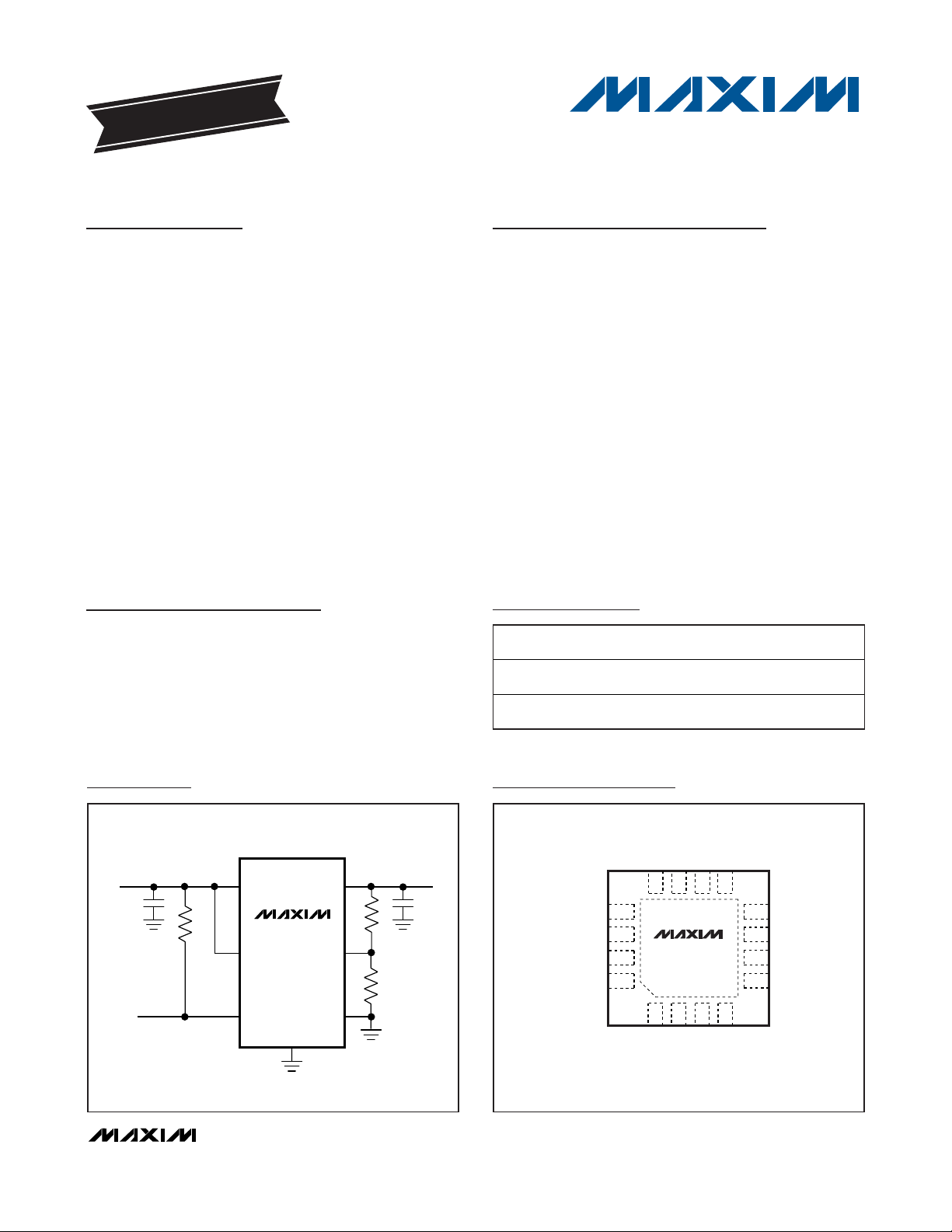
Pin Configuration
Ordering Information
IN
EN
GND
OUT
FB
N.C.
POK
(POR)
V
IN
1.425V TO 3.6V
V
OUT
0.5V TO VIN - 0.2V
MAX8556
(MAX8557)
Typical Operating Circuit
19-3257; Rev 1; 8/08
For pricing, delivery, and ordering information, please contact Maxim Direct at 1-888-629-4642,
or visit Maxim’s website at www.maxim-ic.com.
EVALUATION KIT
AVAILABLE
+
Denotes a lead-free/RoHS-compliant package.
PART TEMP RANGE
MAX8556ETE+ -40°C to +85°C
MAX8557ETE+ -40°C to +85°C
PINPACKAGE
16 Thin QFN
5mm x 5mm
16 Thin QFN
5mm x 5mm
FEATURE
POK
POR
TOP VIEW
GND
N.C.
13
FB
14
15
16
EN
+
OUT
POK (POR)
12 11 10 9
MAX8556
(MAX8557)
1234
IN
IN
THIN QFN
5mm x 5mm
OUT
IN
OUT
IN
OUT
8
OUT
7
IN
6
IN
5

MAX8556/MAX8557
4A Ultra-Low-Input-Voltage
LDO Regulators
2 _______________________________________________________________________________________
ABSOLUTE MAXIMUM RATINGS
ELECTRICAL CHARACTERISTICS
(V
EN
= V
IN
= 1.8V, V
OUT
= 1.5V, I
OUT
= 2mA, TA = -40°C to +85°C, typical values are at TA = +25°C, unless otherwise noted.) (Note 2)
Stresses beyond those listed under “Absolute Maximum Ratings” may cause permanent damage to the device. These are stress ratings only, and functional
operation of the device at these or any other conditions beyond those indicated in the operational sections of the specifications is not implied. Exposure to
absolute maximum rating conditions for extended periods may affect device reliability.
IN, EN, POK, POR to GND .......................................-0.3V to +4V
FB, OUT to GND ..........................................-0.3V to (V
IN
+ 0.3V)
Output Short-Circuit Duration.....................................Continuous
Continuous Power Dissipation (T
A
= +70°C)
16-Pin Thin QFN (derate 33.3mW/°C
above +70°C) (Note 1)............................................2666.7mW
Operating Temperature Range ...........................-40°C to +85°C
Junction Temperature......................................................+150°C
Storage Temperature Range .............................-65°C to +150°C
Lead Temperature (soldering, 10s) .................................+300°C
Note 1: Maximum power dissipation is obtained using JEDEC JESD51-5 and JESD51-7 standards.
IN
Input Voltage Range 1.425 3.600 V
Input Undervoltage Lockout
OUT
Output Voltage Range 0.5 3.4 V
Load Regulation I
Line Regulation V
Dropout Voltage V
Regulated Output-Voltage Current
Limit
Load Capacitance ESR < 50mA 16 120 µF
FB
FB Threshold Accuracy
(Note 3)
FB Input Bias Current V
GND
GND Supply Current
GND Shutdown Current V
POK
FB Power-OK Fault Threshold
POK Output Voltage, Low V
PARAMETER CONDITIONS MIN TYP MAX UNITS
VIN rising, 70mV hysteresis 1.30 1.35 1.40
falling 1.23 1.28 1.33
V
IN
= 2mA to 4A 0.1 %/A
OUT
= 1.425V to 3.6V, V
IN
= 1.425V, I
IN
V
= 3.6V, V
IN
V
= 1.225V to 3V, V
OUT
I
= 2mA to 4A
OUT
= 0.5V, V
FB
V
= 1.425V to 3.6V, V
IN
Dropout, V
IN
FB moving out of regulation,
V
IN
FB
IN
= 3.6V, EN = GND 150 µA
= 1.425V to 3.6V, 10mV hysteresis
= 0.4V or 0.6V, I
= 4A, V
OUT
= 3V, V
OUT
= 3.6V 0.001 1 µA
IN
= 3.6V, V
POK
= 1.225V -0.15 0 +0.15 %/V
OUT
= 480mV 100 200 mV
FB
= 460mV 5 7 9 A
FB
= V
IN
OUT
= 480mV 1000 2000
FB
= 2mA 25 200 mV
+ 0.2V to 3.6V,
OUT
= 1.225V 800 1600
FB high 540 550 560
FB low 440 450 460
495 500 505 mV
V
µA
mV

MAX8556/MAX8557
4A Ultra-Low-Input-Voltage
LDO Regulators
_______________________________________________________________________________________ 3
Note 2: Specifications to TA= -40°C are guaranteed by design and not production tested.
Note 3: Minimum supply voltage for output accuracy must be at least 1.425V.
ELECTRICAL CHARACTERISTICS (continued)
(V
EN
= V
IN
= 1.8V, V
OUT
= 1.5V, I
OUT
= 2mA, TA = -40°C to +85°C, typical values are at TA = +25°C, unless otherwise noted.) (Note 2)
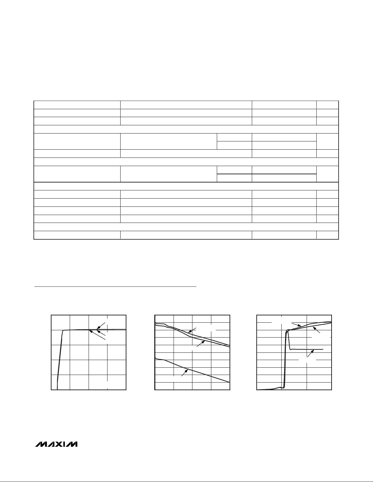
Typical Operating Characteristics
(V
EN
= VIN= +1.8V, V
OUT
= +1.5V, I
OUT
= 4A, C
OUT
= 20µF, CIN= 20µF, and TA= +25°C, unless otherwise noted.)
OUTPUT VOLTAGE vs. INPUT VOLTAGE
MAX8556 toc01
INPUT VOLTAGE (V)
OUTPUT VOLTAGE (V)
3.02.41.8
1.35
1.40
1.45
1.50
1.55
1.30
1.2 3.6
TA = -25°C
T
A
= -40°C
TA = -85°C
I
LOAD
= 2A
OUTPUT VOLTAGE vs. LOAD CURRENT
MAX8556 toc02
LOAD CURRENT (A)
OUTPUT VOLTAGE (V)
321
1.4980
1.4985
1.4990
1.4995
1.5000
1.5005
1.5010
1.5015
1.5020
1.5025
1.4975
04
TA = -40°C
TA = +85°C
TA = +25°C
GND CURRENT vs. INPUT VOLTAGE
MAX8556 toc03
INPUT VOLTAGE (V)
GND CURRENT (μA)
2.41.2
100
200
300
400
500
600
700
800
900
1000
0
0 3.6
I
LOAD
= 4A
I
LOAD
= 2A
I
LOAD
= 0A
PARAMETER CONDITIONS MIN TYP MAX UNITS
POK Output Current, High V
POK Delay Time From FB rising to POK high 25 50 100 µs
EN
Enable Input Threshold V
Enable Input Bias Current V
THERMAL SHUTDOWN
Thermal-Shutdown Threshold Output on and off
POR
FB Power-On Reset Fault Threshold FB falling, V
POR Output Voltage, Low V
POR Output Current, High V
POR Rising Delay Time FB rising to POR high impedance 100 140 200 ms
SOFT-START
Soft-Start Time 100 µs
= 3.6V V
POK
= 1.425V to 3.6V
IN
= 0V or 3.6V -1 +1 µA
EN
= 0.5 0.001 1 µA
FB
EN rising 1.25
EN falling 0.4
TJ rising +160
falling +115
T
J
= 1.425V to 3.6V, 10mV hysteresis 440 450 460 mV
IN
= 0.4V, I
FB
= 3.6V, VFB = 0.5V 0.001 1 µA
POR
= 2mA 25 200 mV
POR
V
°C
 Loading...