

General Description
The MAX8550/MAX8551 integrate a synchronous-buck
PWM controller to generate V
DDQ
, a sourcing and sinking
LDO linear regulator to generate VTT, and a 10mA reference output buffer to generate V
TTR
. The buck controller
drives two external N-channel MOSFETs to generate output voltages down to 0.7V from a 2V to 28V input with output currents up to 15A. The LDO can sink or source up to
1.5A continuous and 3A peak current. Both the LDO output and the 10mA reference buffer output can be made
to track the REFIN voltage. These features make the
MAX8550/MAX8551 ideally suited for DDR memory applications in desktops, notebooks, and graphic cards.
The PWM controller in the MAX8550/MAX8551 utilizes
Maxim’s proprietary Quick-PWM™ architecture with programmable switching frequencies of up to 600kHz. This
control scheme handles wide input/output voltage ratios
with ease and provides 100ns response to load transients while maintaining high efficiency and a relatively
constant switching frequency. The MAX8550 offers fully
programmable UVP/OVP and skip-mode options ideal in
portable applications. Skip mode allows for improved
efficiency at lighter loads. The MAX8551, which is targeted towards desktop and graphic-card applications,
does not offer the pulse-skip feature.
The VTT and VTTR outputs track to within 1% of V
REFIN
/ 2.
The high bandwidth of this LDO regulator allows excellent transient response without the need for bulk capacitors, thus reducing cost and size.
The buck controller and LDO regulators are provided with
independent current limits. Adjustable lossless foldback
current limit for the buck regulator is achieved by monitoring the drain-to-source voltage drop of the low-side MOSFET. Additionally, overvoltage and undervoltage
protection mechanisms are built in. Once the overcurrent
condition is removed, the regulator is allowed to enter
soft-start again. This helps minimize power dissipation
during a short-circuit condition. The MAX8550/MAX8551
allow flexible sequencing and standby power management using the SHDNA, SHDNB, and STBY inputs.
Both the MAX8550 and MAX8551 are available in a
small 5mm × 5mm, 28-pin thin QFN package.
Applications
DDR I and DDR II Memory Power Supplies
Desktop Computers
Notebooks and Desknotes
Graphic Cards
Game Consoles
RAID
Networking
Features
Buck Controller
♦ Quick-PWM with 100ns Load-Step Response
♦ Up to 95% Efficiency
♦ 2V to 28V Input Voltage Range
♦ 1.8V/2.5V Fixed or 0.7V to 5.5V Adjustable Output
♦ Up to 600kHz Selectable Switching Frequency
♦ Programmable Current Limit with Foldback
Capability
♦ 1.7ms Digital Soft-Start and Independent
Shutdown
♦ Overvoltage/Undervoltage-Protection Option
♦ Power-Good Window Comparator
LDO Section
♦ Fully Integrated VTT and VTTR Capability
♦ VTT has ±3A Sourcing/Sinking Capability
♦ VTT and VTTR Outputs Track V
REFIN
/ 2
♦ All-Ceramic Output-Capacitor Designs
♦ 1.0V to 2.8V Input Voltage Range
♦ Power-Good Window Comparator
MAX8550/MAX8551
Integrated DDR Power-Supply Solutions for
Desktops, Notebooks, and Graphic Cards
________________________________________________________________ Maxim Integrated Products 1
PART
TEMP RANGE
PIN-PACKAGE
MAX8550ETI
28 5mm × 5mm TQFN
MAX8550ETI+
28 5mm × 5mm TQFN
MAX8551ETI
28 5mm × 5mm TQFN
Ordering Information
28
27
26
25
24
23
22
8
9
10
11
12
13
14
15
16
17
18
19
20
21
7
6
5
4
3
2
1
MAX8550
MAX8551
5mm x 5mm Thin QFN
TOP VIEW
OVP/UVP
(N.C. FOR
MAX8551)
TON
REF
ILIM
POK1
POK2
STBY
SHDNB
SHDNA
AV
DD
SKIP
(TP1 FOR
M
AX8551)
GND
PGND1
V
DD
DL
BST
LX
DH
V
IN
OUT
FB
REFIN
VTTI
VTT
PGND2
VTTR
VTTS
SS
Pin Configuration
19-3173; Rev 2; 9/04
For pricing, delivery, and ordering information, please contact Maxim/Dallas Direct! at
1-888-629-4642, or visit Maxim’s website at www.maxim-ic.com.
Typical Operating Circuit appears at end of data sheet.
Quick-PWM is a trademark of Maxim Integrated Products, Inc.
+Denotes lead-free package.
查询MAX8550ETI供应商查询MAX8550ETI供应商
-40°C to +85°C
-40°C to +85°C
-40°C to +85°C
PARAMETER
CONDITIONS
UNITS
MAIN PWM CONTROLLER
V
IN
228
Input Voltage Range
4.5 5.5
V
Output Adjust Range V
OUT
0.7 5.5 V
FB = OUT
0.7
FB = GND
2.5
Output Voltage Accuracy
(Note 2)
FB = V
DD
1.8
V
Soft-Start Ramp Time t
SS
Rising edge of SHDNA to full current limit 1.7 ms
TON = GND (600kHz)
219
TON = REF (450kHz)
273
389
On-Time t
ON
VIN = 15V,
V
OUT
= 1.5V
(Note 3)
571
ns
Minimum Off-Time
(Note 3)
450 ns
VIN Quiescent Supply Current I
IN
25 40 µA
VIN Shutdown Supply Current SHDNA = SHDNB = GND 1 5 µA
All on (PWM, VTT, and VTTR on) 2.5 5
SHDNA = GND (only VTT and VTTR on) 2 4
STBY = AVDD (only VTTR and PWM on) 1 2
AVDD Quiescent Supply Current I
AVDD
SHDNB = GND (only PWM on) 0.5 1
mA
AVDD + VDD Shutdown Supply
Current
SHDNA = SHDNB = GND 2 10 µA
Rising edge of V
IN
4.1
4.4 V
AVDD Undervoltage-Lockout
Threshold
Hysteresis 50 mV
VDD Quiescent Supply Current I
VDD
Set VFB = 0.8V 1 5 µA
MAX8550/MAX8551
Integrated DDR Power-Supply Solutions for
Desktops, Notebooks, and Graphic Cards
2 _______________________________________________________________________________________
ABSOLUTE MAXIMUM RATINGS
ELECTRICAL CHARACTERISTICS
(VIN= +15V, VDD= AVDD= V
SHDNA
= V
SHDNB
= V
BST
= V
ILIM
= 5V, V
OUT
= V
REFIN
= V
VTTI
= 2.5V, UVP/OVP = STBY = FB = SKIP
= GND, PGND1 = PGND2 = LX = GND, TON = OPEN, V
VTTS
= V
VTT
, TA= -40°C to +85°C, unless otherwise noted. Typical values
are at T
A
= +25°C.) (Note 1)
Stresses beyond those listed under “Absolute Maximum Ratings” may cause permanent damage to the device. These are stress ratings only, and functional
operation of the device at these or any other conditions beyond those indicated in the operational sections of the specifications is not implied. Exposure to
absolute maximum rating conditions for extended periods may affect device reliability.
VINto GND .............................................................-0.3V to +30V
V
DD, AVDD
, VTTI to GND.........................................-0.3V to +6V
SHDNA, SHDNB, REFIN to GND..............................-0.3V to +6V
SS, POK1, POK2, SKIP, ILIM, FB to GND................-0.3V to +6V
STBY, TON, REF, UVP/OVP to GND........-0.3V to (AV
DD
+ 0.3V)
OUT, VTTR to GND..................................-0.3V to (AV
DD
+ 0.3V)
DL to PGND1..............................................-0.3V to (V
DD
+ 0.3V)
DH to LX....................................................-0.3V to (V
BST
+ 0.3V)
LX to BST..................................................................-6V to +0.3V
LX to GND .................................................................-2V to +30V
VTT to GND...............................................-0.3V to (V
VTTI
+ 0.3V)
VTTS to GND............................................-0.3V to (AV
DD
+ 0.3V)
PGND1, PGND2 to GND.......................................-0.3V to +0.3V
REF Short Circuit to GND...........................................Continuous
Continuous Power Dissipation (T
A
= +70°C)
28-Pin 5mm x 5mm TQFN (derate 35.7mW/°C
above +70°C).................................................................2.86W
Operating Temperature Range ...........................-40°C to +85°C
Junction Temperature......................................................+150°C
Storage Temperature Range.............................-65°C to +165°C
Lead Temperature (soldering, 10s).................................+300°C
SYMBOL
MIN TYP MAX
VDD, AV
t
OFF_MIN
DD
0.693
2.47
1.78
TON = OPEN (300kHz) 316 352
TON = AVDD (200kHz) 461 516
170 194
213 243
200 300
4.25
0.707
2.53
1.82
MAX8550/MAX8551
Integrated DDR Power-Supply Solutions for
Desktops, Notebooks, and Graphic Cards
_______________________________________________________________________________________ 3
PARAMETER
SYMBOL
CONDITIONS
MIN
TYP
MAX
UNITS
REFERENCE
Reference Voltage V
REF
AVDD = 4.5V to 5.5V; I
REF
= 0
2
V
Reference Load Regulation I
REF
= 0 to 50µA
V
V
REF
rising
V
REF Undervoltage Lockout
Hysteresis
mV
FAULT DETECTION
OVP Trip Threshold
UVP/OVP = AVDD (Note 4)
120 %
UVP Trip Threshold
(Referred to Nominal V
OUT
)
65 70 75 %
Lower level, falling edge, 1% hysteresis 87 90 93
POK1 Trip Threshold
(Referred to Nominal V
OUT
)
Upper level, rising edge, 1% hysteresis
113
%
Lower level, falling edge, 1% hysteresis
90
POK2 Trip Threshold
(Referred to Nominal V
VTTS
and V
VTTR
)
Upper level, rising edge, 1% hysteresis
%
UVP Blanking Time From rising edge of SHDNA 10 20 40 ms
OVP, UVP, POK_ Propagation
Delay
OVP not applicable in MAX8551 10 µs
POK_ Output Low Voltage I
SINK
= 4mA 0.3 V
POK_ Leakage Current V
POK_
= 5.5V, VFB = 0.8V, V
VTTS
= 1.3V 1 µA
ILIM Adjustment Range V
ILIM
V
ILIM Input Leakage Current 0.1 µA
Current-Limit Threshold (Fixed)
PGND1 to LX
45 50 55 mV
Current-Limit Threshold
(Adjustable) PGND1 to LX
V
ILIM
= 2V
235 mV
Current-Limit Threshold (Negative
Direction) PGND1 to LX
SKIP = AV
DD
(Note 4) -75 -60 -45 mV
Current-Limit Threshold (Negative
Direction) PGND1 to LX
SKIP = AV
DD
, V
ILIM
= 2V (Note 4)
mV
Zero-Crossing Detection
Threshold PGND1 to LX
3mV
Thermal-Shutdown Threshold
°C
Thermal-Shutdown Hysteresis 15 °C
ELECTRICAL CHARACTERISTICS (continued)
(VIN= +15V, VDD= AVDD= V
SHDNA
= V
SHDNB
= V
BST
= V
ILIM
= 5V, V
OUT
= V
REFIN
= V
VTTI
= 2.5V, UVP/OVP = STBY = FB = SKIP
= GND, PGND1 = PGND2 = LX = GND, TON = OPEN, V
VTTS
= V
VTT
, TA= -40°C to +85°C, unless otherwise noted. Typical values
are at T
A
= +25°C.) (Note 1)
(Referred to Nominal V
OUT
)
1.98
1.93
300
112 116
107 110
87.5
107.5 110 112.5
2.02
0.01
92.5
0.25 2.00
170 200
-250
+160
MAX8550/MAX8551
Integrated DDR Power-Supply Solutions for
Desktops, Notebooks, and Graphic Cards
4 _______________________________________________________________________________________
PARAMETER
SYMBOL
CONDITIONS
MIN
TYP
MAX
UNITS
MOSFET DRIVERS
DH Gate-Driver On-Resistance V
BST
- VLX = 5V 1 4 Ω
DL Gate-Driver On-Resistance in
High State
14Ω
DL Gate-Driver On-Resistance in
Low State
0.5 3 Ω
DH falling to DL rising 30
Dead Time (Additional to
Adaptive Delay)
DL falling to DH rising 30
ns
INPUTS AND OUTPUTS
Rising edge
1.7
V
Logic Input Threshold
(SHDN_, STBY, SKIP (Note 4))
Hysteresis
mV
Logic Input Current
(SHDN_, STBY, SKIP (Note 4))
-1 +1 µA
Low (2.5V output)
Dual-Mode™ Input Logic
Levels (FB)
High (1.8V output) 2.1
V
Input Bias Current (FB)
µA
High
AV
DD
-
0.4
Floating
REF
Four-Level Input Logic Levels
(TON, OVP/UVP (Note 4))
Low 0.5
V
Logic Input Current
(TON, OVP/UVP (Note 4))
-3 +3 µA
FB = GND 90
350
FB = AV
DD
70
270OUT Input Resistance
FB adjustable mode
kΩ
OUT Discharge-Mode
On-Resistance
(Note 4) 10 25 Ω
DL Turn-On Level During
Discharge Mode
(Measured at OUT)
(Note 4) 0.3 V
ELECTRICAL CHARACTERISTICS (continued)
(VIN= +15V, VDD= AVDD= V
SHDNA
= V
SHDNB
= V
BST
= V
ILIM
= 5V, V
OUT
= V
REFIN
= V
VTTI
= 2.5V, UVP/OVP = STBY = FB = SKIP
= GND, PGND1 = PGND2 = LX = GND, TON = OPEN, V
VTTS
= V
VTT
, TA= -40°C to +85°C, unless otherwise noted. Typical values
are at T
A
= +25°C.) (Note 1)
Dual Mode is a trademark of Maxim Integrated Products, Inc.
1.20
225
-0.1 +0.1
3.15 3.85
1.65 2.35
175
135
400 800 1600
2.20
0.05
MAX8550/MAX8551
Integrated DDR Power-Supply Solutions for
Desktops, Notebooks, and Graphic Cards
_______________________________________________________________________________________ 5
Note 1: Specifications to -40°C are guaranteed by design, not production tested.
Note 2: When the inductor is in continuous conduction, the output voltage has a DC regulation level higher than the error-compara-
tor threshold by 50% of the ripple. In discontinuous conduction, the output voltage has a DC regulation level higher than the
trip level by approximately 1.5% due to slope compensation.
Note 3: On-time and off-time specifications are measured from 50% point to 50% point at the DH pin with LX = GND, V
BST
= 5V,
and a 250pF capacitor connected from DH to LX. Actual in-circuit times may differ due to MOSFET switching speeds.
Note 4: Not applicable to the MAX8551.
PARAMETER
CONDITIONS
UNITS
LINEAR REGULATORS (VTTR AND VTT)
VTTI Input Voltage Range V
VTTI
1 2.8 V
VTTI Supply Current I
VTTI
I
VTT
= I
VTTR
= 0
1mA
VTTI Shutdown Current SHDNA = SHDNB = GND 10 µA
REFIN Input Impedance V
REFIN
= 2.5V 12 20 30 kΩ
REFIN Range V
REFIN
1
V
V
REFIN
rising 0.7 0.9 V
REFIN Lockout Threshold
Hysteresis 75 mV
Soft-Start Charge Current I
SS
VSS = 0 4 µA
VTT Internal MOSFET High-Side
On-Resistance
I
VTT
= -100mA, V
VTTI
= 1.5V,
AV
DD
= 4.5V
0.3 Ω
VTT Internal MOSFET Low-Side
On-Resistance
I
VTT
= 100mA, AVDD = 4.5V 0.3 Ω
VTT Output Accuracy
(Referred to V
REFIN
/ 2)
V
REFIN
= 1.5V or 2.5V, I
VTT
= 1mA -1 +1 %
V
REFIN
= 2.5V, I
VTT
= 0 to ±1.5A 1
VTT Load Regulation
V
REFIN
= 1.5V, I
VTT
= 0 to ±1A 1
%
VTT Current Limit VTT = 0 or VTTI ±3 ±5
A
VTTS Input Current I
VTTS
V
VTTS
= 1.5V, VTT open
1µA
VTTR Output Error
(Referred to V
REFIN
/ 2)
V
REFIN
= 1.5V or 2.5V, I
VTTR
= 0 -1 +1 %
VTTR Current Limit V
VTTR
= 0 or V
VTTI
mA
ELECTRICAL CHARACTERISTICS (continued)
(VIN= +15V, VDD= AVDD= V
SHDNA
= V
SHDNB
= V
BST
= V
ILIM
= 5V, V
OUT
= V
REFIN
= V
VTTI
= 2.5V, UVP/OVP = STBY = FB = SKIP
= GND, PGND1 = PGND2 = LX = GND, TON = OPEN, V
VTTS
= V
VTT
, TA= -40°C to +85°C, unless otherwise noted. Typical values
are at T
A
= +25°C.) (Note 1)
SYMBOL
MIN TYP MAX
<0.1
2.8
±6.5
0.1
±23 ±40 ±60
MAX8550/MAX8551
Integrated DDR Power-Supply Solutions for
Desktops, Notebooks, and Graphic Cards
6 _______________________________________________________________________________________
Typical Operating Characteristics
(V
VIN
= 12V, V
OUT
= 2.5V, TON = GND, SKIP = AVDD, circuit of Figure 8, TA= +25°C, unless otherwise noted.)
EFFICIENCY vs. LOAD CURRENT
(TON = GND)
MAX8550/51 toc01
I
LOAD
(A)
EFFICIENCY (%)
1010.1
60
70
80
90
100
50
10
20
30
40
0
0.01 100
fSW = 600kHz
V
OUT
= 2.5V
V
OUT
= 1.8V
V
OUT
= 1.5V
SKIP = GND
SKIP = AV
DD
EFFICIENCY vs. LOAD CURRENT
(TON = OPEN)
MAX8550/51 toc02
I
LOAD
(A)
EFFICIENCY (%)
1010.1
10
20
30
40
50
60
70
80
90
100
0
0.01 100
fSW = 300kHz
V
OUT
= 2.5V
V
OUT
= 1.8V
V
OUT
= 1.5V
SKIP = GND
SKIP = AV
DD
SWITCHING FREQUENCY vs. LOAD CURRENT
(TON = GND)
MAX8550/51 toc03
I
LOAD
(A)
FREQUENCY (kHz)
11108 92 3 4 5 6 71
50
100
150
200
250
300
350
400
450
500
550
600
650
700
0
012
SKIP = GND
SKIP = AV
DD
SWITCHING FREQUENCY vs. INPUT VOLTAGE
(TON = GND)
MAX8550/51 toc04
VIN (V)
FREQUENCY (kHz)
262420 228 10 12 14 16 186
420
440
460
480
500
540
520
560
580
600
620
640
660
680
700
400
428
I
LOAD
= 12A
I
LOAD
= 0A
SWITCHING FREQUENCY vs. TEMPERATURE
(TON = GND)
MAX8550/51 toc05
TEMPERATURE (°C)
FREQUENCY (kHz)
80655035205-10-25
650
660
670
680
690
700
600
640
630
620
610
-40
I
LOAD
= 12A
OUTPUT VOLTAGE
vs. LOAD CURRENT
MAX8550/51 toc06
I
LOAD
(A)
V
OUT
(V)
12106 842
2.495
2.500
2.505
2.510
2.515
2.520
2.525
2.530
2.535
2.540
2.490
014
VIN = 15V,
TON = GND
SKIP = GND
SKIP = AV
DD
VTT VOLTAGE
vs. VTT CURRENT
MAX8550/51 toc07
I
VTT
(A)
V
VTT
(V)
21-2 -1 0
1.21
1.22
1.23
1.24
1.25
1.26
1.27
1.28
1.20
-3 3
VTTR VOLTAGE
vs. VTTR CURRENT
MAX8550/51 toc08
I
VTTR
(mA)
V
VTTR
(V)
105-10 -5 0
1.21
1.22
1.23
1.24
1.25
1.26
1.27
1.28
1.20
-15 15
LINE REGULATION
(V
OUT
vs. VIN)
MAX8550/51 toc09
VIN (V)
V
OUT
(
V
)
262420 228 10 12 14 16 186
2.46
2.47
2.48
2.49
2.50
2.51
2.52
2.53
2.54
2.55
2.45
428
I
LOAD
= 0A
I
LOAD
= 12A
MAX8550/MAX8551
Integrated DDR Power-Supply Solutions for
Desktops, Notebooks, and Graphic Cards
_______________________________________________________________________________________ 7
LOAD TRANSIENT (BUCK)
MAX8550/51 toc10
20µs/div
12A
V
OUT
100mV/div
VTT
100mV/div
VTTR
100mV/div
I
LOAD
10A/div
0.1A
I
VTT
= 1.5A, I
VTTR
= 15mA
LOAD TRANSIENT VTT (-1.5A TO +1.5A)
MAX8550/51 toc11
40µs/div
V
OUT
50mV/div
VTT
50mV/div
VTTR
50mV/div
I
VTT
2A/div
0A
I
LOAD
= 12A, I
VTTR
= 15mA
LOAD TRANSIENT VTT (-3A TO +3A)
MAX8550/51 toc12
40µs/div
V
OUT
50mV/div
VTT
50mV/div
VTTR
50mV/div
I
VTT
5A/div
0A
I
LOAD
= 12A, I
VTTR
= 15mA
POWER-UP WAVEFORMS
MAX8550/51 toc13
200µs/div
OUT
1V/div
VTT
2V/div
VTTR
1V/div
V
IN
10V/div
0V
0V
0V
0V
VDD = 5V, I
LOAD
= 12A, I
VTT
= 1.5A, I
VTTR
= 15mA
POWER-DOWN WAVEFORMS
MAX8550/51 toc14
200µs/div
OUT
1V/div
VTT
2V/div
VTTR
1V/div
V
IN
10V/div
0V
0V
0V
0V
VDD = 5V, I
LOAD
= 12A, I
VTT
= 1.5A, I
VTTR
= 15mA
V
DDQ
STARTUP AND SHUTDOWN INTO
HEAVY LOAD, DISCHARGE DISABLED
MAX8550/51 toc15
1ms/div
V
OUT
2V/div
VTT
1V/div
SHDNA + SHDNB
5V/div
POK1
5V/div
0V
0V
0V
0V
I
LOAD
= 12A,
I
VTT
= 1.5A
Typical Operating Characteristics (continued)
(V
VIN
= 12V, V
OUT
= 2.5V, TON = GND, SKIP = AVDD, circuit of Figure 8, TA= +25°C, unless otherwise noted.)
V
DDQ
STARTUP AND SHUTDOWN INTO
LIGHT LOAD, DISCHARGE ENABLED
MAX8550/51 toc16
2ms/div
V
OUT
1V/div
VTT
1V/div
SHDNA + SHDNB
5V/div
POK1
5V/div
0V
0V
0V
0V
R
LOAD
= 10Ω,
R
VTT
= 20Ω
VTT, VTTR STARTUP AND SHUTDOWN
MAX8550/51 toc17
200µs/div
VTT
1V/div
VTTR
1V/div
SHDNB
5V/div
POK2
5V/div
0V
0V
0V
0V
I
VTT
= 1.5A, I
VTTR
= 15mA
MAX8550/MAX8551
Integrated DDR Power-Supply Solutions for
Desktops, Notebooks, and Graphic Cards
8 _______________________________________________________________________________________
OVERVOLTAGE AND TURN-OFF
OF BUCK OUTPUT
MAX8550/51 toc18
20µs/div
V
OUT
2V/div
I
L
25A/div
DL
5V/div
DH
20V/div
0V
0V
0V
0A
Typical Operating Characteristics (continued)
(V
VIN
= 12V, V
OUT
= 2.5V, TON = GND, SKIP = AVDD, circuit of Figure 8, TA= +25°C, unless otherwise noted.)
SHORT CIRCUIT AND
RECOVERY OF V
DDQ
MAX8550/51 toc19
400µs/div
V
OUT
2V/div
I
LOAD
10A/div
V
IN
10V/div
I
IN
2A/div
0A
0V
0A
0V
UVP DISABLED, FOLDBACK CURRENT LIMIT
SHORT CIRCUIT AND
RECOVERY OF V
DDQ
MAX8550/51 toc20
400µs/div
V
OUT
2V/div
I
LOAD
10A/div
V
IN
10V/div
I
IN
2A/div
0A
0V
0A
0V
UVP ENABLED
SHORT CIRCUIT OF VTT
MAX8550/51 toc21
400µs/div
VTT
1V/div
I
VTT
5A/div
0A
0V
MAX8550/MAX8551
Integrated DDR Power-Supply Solutions for
Desktops, Notebooks, and Graphic Cards
_______________________________________________________________________________________ 9
Pin Description
PIN NAME FUNCTION
1TON
On-Time Selection-Control Input. This four-level logic input sets the nominal DH on-time. Connect to
GND, REF, AV
DD
, or leave TON unconnected to select the following nominal switching frequencies:
TON = AV
DD
(200kHz)
TON = OPEN (300kHz)
TON = REF (450kHz)
TON = GND (600kHz)
OVP/
UVP
Overvoltage/Undervoltage-Protection Control Input. This four-level logic input enables or disables the
overvoltage and/or undervoltage protection. The overvoltage limit is 116% of the nominal output
voltage. The undervoltage limit is 70% of the nominal output voltage. Discharge mode is enabled when
OVP is also enabled. Connect the OVP/UVP pin to the following pins for the desired function:
OVP/UVP = AV
DD
(Enable OVP and discharge mode, enable UVP.)
OVP/UVP = OPEN (Enable OVP and discharge mode, disable UVP.)
OVP/UVP = REF (Disable OVP and discharge mode, enable UVP.)
OVP/UVP = GND (Disable OVP and discharge mode, disable UVP.)
2
N.C.
Do not connect; leave open.*
3 REF
+2.0V Reference Voltage Output. Bypass to GND with a 0.1µF (min) capacitor. REF can supply 50µA
for external loads. Can be used for setting voltage for ILIM. REF turns off when SHDNA, SHDNB, and
STBY are low.
4 ILIM
Valley Current-Limit Threshold Adjustment for Buck Regulator. The current-limit threshold across PGND
and LX is 0.1 times the voltage at ILIM. Connect ILIM to a resistive divider, typically from REF to GND,
to set the current-limit threshold between 25mV and 200mV. This corresponds to a 0.25V to 2V range at
ILIM. Connect ILIM to AV
DD
to select the 50mV default current-limit threshold. See the Setting the
Current Limit section.
5 POK1
Buck Power-Good Open-Drain Output. POK1 is low when the buck output voltage is more than 10%
above or below the normal regulation point or during soft-start. POK1 is high impedance when the
output is in regulation and the soft-start circuit has terminated. POK1 is low in shutdown.
6 POK2
LDO Power-Good Open-Drain Output. In normal mode, POK2 is low when either VTTR or VTTS is more
than 10% above or below the normal regulation point, which is typically REFIN / 2. In standby mode,
POK2 responds only to the VTTR input. POK2 is low in shutdown, and when V
REFIN
is less than 0.8V.
7 STBY
Standby. Connect to high for low-quiescent mode where the VTT output is disabled, but the VTTR
buffer is kept alive if SHDNB is high. POK2 takes input from only VTTR in this mode. PWM output can
be on or off, depending on the state of SHDNA.
8SS
Soft-Start Control for VTT and VTTR. Connect a capacitor (C9 in the Typical Applications Circuit) from
SS to ground (see the Soft-Start Capacitor Selection section). Leave SS open to disable soft-start.
SS discharges to ground when SHDNB is low. See the POR, UVLO, and Soft-Start section.
9 VTTS
Sensing Pin for Termination Supply Output. Normally connected to VTT pin to allow accurate regulation
to half the REFIN voltage. Connected to a resistive divider from VTT to GND to regulate VTT to higher
than half the REFIN voltage.
10 VTTR Termination Reference Voltage. VTTR tracks V
REFIN
/ 2.
*The MAX8551 has no OVP or discharge-mode feature. Only UVP is available.
(MAX8550)
(MAX8551)
MAX8550/MAX8551
Integrated DDR Power-Supply Solutions for
Desktops, Notebooks, and Graphic Cards
10 ______________________________________________________________________________________
Pin Description (continued)
PIN NAME FUNCTION
11 PGND2 Power Ground for VTT and VTTR. Connect PGND2 externally to the underside of the exposed pad.
12 VTT Termination Power-Supply Output. Connect VTT to VTTS to regulate to V
REFIN
/ 2.
13 VTTI
Power-Supply Input Voltage for VTT and VTTR. Normally connected to the output of the buck regulator
for DDR application.
14 REFIN External Reference Input. This is used to regulate the VTT and VTTR outputs to V
REFIN
/ 2.
15 FB
Feedback Input for Buck Output. Connect to AV
DD
for a +1.8V fixed output or to GND for a +2.5V fixed
output. For an adjustable output (0.7V to 5.5V), connect FB to a resistive divider from the output
voltage. FB regulates to +0.7V.
16 OUT
Output-Voltage Sense Connection. Connect to the positive terminal of the buck output filter capacitor.
OUT senses the output voltage to determine the on-time for the high-side switching MOSFET (Q1 in the
Typical Applications Circuit). OUT also serves as the buck output’s feedback input in fixed-output
modes. When discharge mode is enabled by OVP/UVP, the output capacitor is discharged through an
internal 10Ω resistor connected between OUT and GND.
17 V
IN
Input-Voltage Sense Connection. Connect to input power source. VIN is used only to set the PWM’s ontime one-shot timer. IN voltage range is from 2V to 28V.
18 DH High-Side Gate-Driver Output. Swings from LX to BST. DH is low when in shutdown or UVLO.
19 LX
External Inductor Connection. Connect LX to the input side of the inductor. LX is used for both current
limit and the return supply of the DH driver.
20 BST
Boost Flying-Capacitor Connection. Connect to an external capacitor and diode according to the
Typical Applications Circuit (Figure 8). See the Boost-Supply Diode and Capacitor Selection section.
21 DL Synchronous-Rectifier Gate-Driver Output. Swings from PGND to VDD.
22 V
DD
Supply Input for the DL Gate Drive. Connect to the +4.5V to +5.5V system supply voltage. Bypass to
PGND1 with a 1µF (min) ceramic capacitor.
23 PGND1 Power Ground for Buck Controller. Connect PGND1 externally to the underside of the exposed pad.
24 GND
Analog Ground for Both Buck and LDO. Connect GND externally to the underside of the exposed pad.
SKIP
Pulse-Skipping Control Input. Connect to AVDD for low-noise, forced-PWM mode. Connect to GND to
enable pulse-skipping operation.
25
TP1
In the MAX8551, this pin is a test pin and must be connected to GND (pin 24).
26 AV
DD
Analog Supply Input for Both Buck and LDO. Connect to the +4.5V to +5.5V system supply voltage
with a series 10Ω resistor. Bypass to GND with a 1µF or greater ceramic capacitor.
27 SHDNA
Shutdown Control Input A. Use to control buck output. A rising edge on SHDNA clears the overvoltage
and undervoltage-protection fault latches (see Tables 2 and 3). Connect to AVDD for normal operation.
28 SHDNB
Shutdown Control Input B. Use to control VTT and VTTR outputs. Both VTTR and VTT are high
impedence in shutdown (see Table 2).
(MAX8550)
(MAX8551)

MAX8550/MAX8551
Integrated DDR Power-Supply Solutions for
Desktops, Notebooks, and Graphic Cards
______________________________________________________________________________________ 11
MAX8550/
MAX8551
S
R
Q
S
R
Q
ON-TIME
COMPUTE
t
ON
ONE-SHOT
1.0V
LX
LX
1.16 x INTREF
OVP/UVP
LATCH
QUAD LEVEL
DECODE
20ms
TIMER
0.7 x INTREF
INTREF
FB
DECODE
DISCHARGE
LOGIC
N
2V
REFERENCE
INTREF
V
OUT
= 1.8V
V
OUT
= 2.5V
N
INTREF + 10%
INTREF - 10%
N
POWER-DOWN*
*POWER-DOWN
FORCES POK2 LOW
AND VTT, VTTR TO
HIGH IMPEDANCE.
+0.4V
10kΩ 10kΩ
REFIN
/
2
REFIN
/
2 - 10%
REFIN
/
2 + 10%
REFIN
/
2 - 10%
REFIN
/
2 + 10%
IN
BST
DH
LX
V
DD
DL
PGND
ILIM
V
DD
- 1V
OUT
AV
DD
GND
REF
REFIN
VTT
V
DD
V
DD
N
N
PGND2
VTTR
SS
POK2
FB
POK1
OVP/UVP
(N.C. IN MAX8551)
TON
t
OFF
Q
TRIG
ONE-SHOT
Q
TRIG
ZERO CROSSING
VTTS
VTTI
CURRENT
LIMITS
VTT ILIM
VTTR ILIM
STBY
SHUTDOWN
DECODER
BUCK ON/OFF
VTT ON/OFF VTTR ON/OFF
BIAS ON/OFF
SHDNA
SHDNB
SKIP
(TP1 IN MAX8551
MUST BE CONNECTED TO GND)
VTTI
PGND2
OUT
Figure 1. Functional Diagram

MAX8550/MAX8551
Integrated DDR Power-Supply Solutions for
Desktops, Notebooks, and Graphic Cards
12 ______________________________________________________________________________________
Detailed Description
The MAX8550/MAX8551 combine a synchronous-buck
PWM controller, an LDO linear regulator, and a 10mA reference output buffer. The buck controller drives two external N-channel MOSFETs to deliver load currents up to
12A and generate voltages down to 0.7V from a +2V to
+28V input. The LDO linear regulator can sink and source
up to 1.5A continuous and 3A peak current with relatively
fast response. These features make the MAX8550/
MAX8551 ideally suited for DDR memory applications.
The MAX8550/MAX8551 buck regulator is equipped
with a fixed switching frequency of up to 600kHz using
Maxim’s proprietary constant on-time Quick-PWM
architecture. This control scheme handles wide
input/output voltage ratios with ease, and provides
100ns “instant-on” response to load transients, while
maintaining high efficiency with relatively constant
switching frequency.
The buck controller, LDO, and a reference output
buffer are provided with independent current limits.
Lossless foldback current limit in the buck regulator is
achieved by monitoring the drain-to-source voltage
drop of the low-side FET. The ILIM input is used to
adjust this current limit. Overvoltage protection, if
selected, is achieved by latching the low-side synchronous FET on and the high-side FET off when the output
voltage is over 116% of its set output. It also features
an optional undervoltage protection by latching the
MOSFET drivers to the OFF state during an overcurrent
condition, when the output voltage is lower than 70% of
the regulated output. This helps minimize power dissipation during a short-circuit condition.
The current limit in the LDO and buffered reference output buffer is ±5A and ±40mA, respectively, and neither
have the over- or undervoltage protection. When the
current limit in either output is reached, the output no
longer regulates the voltage, but regulates the current
to the value of the current limit.
+5V Bias Supply (VDDand AVDD)
The MAX8550/MAX8551 require an external +5V bias
supply in addition to the input voltage (VIN). Keeping the
bias supply external to the IC improves the efficiency
and eliminates the cost associated with the +5V linear
regulator that would otherwise be needed to supply the
PWM circuit and the gate drivers. If stand-alone capability is needed, then the +5V supply can be generated with
an external linear regulator such as the MAX1615. VDD,
AVDD, and IN can be connected together if the input
source is a fixed +4.5V to +5.5V supply.
VDDis the supply input for the buck regulator’s MOSFET
drivers, and AVDDsupplies the power for the rest of
the IC. The current from the AVDDand VDDpower
supply must supply the current for the IC and the gate
drive for the MOSFETs. This maximum current can be
estimated as:
where I
VDD
+ I
AVDD
are the quiescent supply currents
into VDDand AVDD, QG1and QG2are the total gate
charges of MOSFETs Q1 and Q2 (at VGS= 5V) in the
Typical Applications Circuit, and fSWis the switching
frequency.
Free-Running Constant-On-Time PWM
The Quick-PWM control architecture is a pseudo-fixedfrequency, constant on-time, current-mode regulator
with voltage feed-forward (Figure 1). This architecture
relies on the output filter capacitor’s ESR to act as a
current-sense resistor, so the output ripple voltage provides the PWM ramp signal. The control algorithm is
simple: the high-side switch on-time is determined
solely by a one-shot whose pulse width is inversely proportional to input voltage and directly proportional to
the output voltage. Another one-shot sets a minimum
off-time of 300ns (typ). The on-time one-shot is triggered if the error comparator is low, the low-side switch
current is below the valley current-limit threshold, and
the minimum off-time one-shot has timed out.
On-Time One-Shot (TON)
The heart of the PWM core is the one-shot that sets the
high-side switch on-time. This fast, low-jitter, adjustable
one-shot includes circuitry that varies the on-time in
response to input and output voltages. The high-side
switch on-time is inversely proportional to the input voltage (VIN) and is proportional to the output voltage:
where K (the switching period) is set by the TON input
connection (Table 1) and R
DS(ON)Q2
is the on-resistance of the synchronous rectifier (Q2) in the Typical
Applications Circuit (Figure 8). This algorithm results in
a nearly constant switching frequency despite the lack
of a fixed-frequency clock generator. The benefits of a
constant switching frequency are twofold:
1) The frequency can be selected to avoid noise-sensi-
tive regions such as the 455kHz IF band.
tK
VI R
V
ON
OUT LOAD DS ON Q
IN
()
=×
+×
()
2
IIIfQQ
BIAS VDD AVDD
SW
GG
=+ +×+
()
12
2) The inductor ripple-current operating point remains
relatively constant, resulting in an easy design
methodology and predictable output voltage ripple.
The on-time one-shot has good accuracy at the operating points specified in the Electrical Characteristics
table (approximately ±12.5% at 600kHz and 450kHz,
and ±10% at 200kHz and 300kHz). On-times at operating points far removed from the conditions specified in
the Electrical Characteristics table can vary over a
wider range. For example, the 600kHz setting typically
runs approximately 10% slower with inputs much
greater than 5V due to the very short on-times required.
The constant on-time translates only roughly to a constant switching frequency. The on-times guaranteed in
the Electrical Characteristics table are influenced by
resistive losses and by switching delays in the highside MOSFET. Resistive losses, which include the
inductor, both MOSFETs, the output capacitor’s ESR,
and any PC board copper losses in the output and
ground, tend to raise the switching frequency as the
load increases. The dead-time effect increases the
effective on-time, reducing the switching frequency as
one or both dead times are added to the effective ontime. The dead time occurs only in PWM mode (SKIP =
VDD) and during dynamic output-voltage transitions
when the inductor current reverses at light or negative
load currents. With reversed inductor current, the inductor’s EMF causes LX to go high earlier than normal,
extending the on-time by a period equal to the DH-rising
dead time. For loads above the critical conduction point,
where the dead-time effect is no longer a factor, the
actual switching frequency is:
where V
DROP1
is the sum of the parasitic voltage drops
in the inductor discharge path, including the synchronous rectifier, the inductor, and any PC board resistances; V
DROP2
is the sum of the resistances in the
charging path, including the high-side switch (Q1 in the
Typical Applications Circuit), the inductor, and any PC
board resistances, and t
ON
is the one-shot on-time (see
the On-Time One-Shot (TON) section.
Automatic Pulse-Skipping Mode
(
SKIP
= GND)
In skip mode (SKIP = GND), an inherent automatic
switchover to PFM takes place at light loads (Figure 2).
This switchover is affected by a comparator that truncates the low-side switch on-time at the inductor current’s zero crossing. The zero-crossing comparator
differentially senses the inductor current across the
synchronous-rectifier MOSFET (Q2 in the Typical
Applications Circuit, Figure 8). Once V
PGND
- V
LX
drops below 5% of the current-limit threshold (2.5mV
for the default 50mV current-limit threshold), the comparator forces DL low (Figure 1). This mechanism causes the threshold between pulse-skipping PFM and
nonskipping PWM operation to coincide with the
boundary between continuous and discontinuous
inductor-current operation (also known as the critical
conduction point). The load-current level at which
PFM/PWM crossover occurs, I
LOAD(SKIP)
, is equal to
half the peak-to-peak ripple current, which is a function
of the inductor value (Figure 2). This threshold is relatively constant, with only a minor dependence on the
input voltage (VIN):
where K is the on-time scale factor (see Table 1). For
example, in the Typical Applications Circuit of Figure 8
(K = 1.7µs, V
OUT
= 2.5V, VIN= 12V, and L = 1µH), the
pulse-skipping switchover occurs at:
The crossover point occurs at an even lower value if a
swinging (soft-saturation) inductor is used. The switching waveforms can appear noisy and asynchronous
when light loading causes pulse-skipping operation,
but this is a normal operating condition that results in
high light-load efficiency. Trade-offs in PFM noise vs.
25 17
21
12 2
12
168
. .
.
VsHV
V
A
×
×
⎛
⎝
⎜
⎞
⎠
⎟
⎛
⎝
⎜
⎞
⎠
⎟
=
µ
µ
- .5V
I
VK
L
VV
V
LOAD SKIP
OUT IN OUT
IN
()
=
×
⎛
⎝
⎜
⎞
⎠
⎟
⎛
⎝
⎜
⎞
⎠
⎟
2
-
f
VV
tV V
SW
OUT DROP
ON IN DROP
=
+
+
()
1
2
MAX8550/MAX8551
Integrated DDR Power-Supply Solutions for
Desktops, Notebooks, and Graphic Cards
______________________________________________________________________________________ 13
Table 1. Approximate K-Factor Errors
TON SETTING
TYPICAL
K-
FACTOR
(µs)
K-FACTOR
ERROR
(%)
MINIMUM V
IN
AT
V
OUT
= 2.5V
(h = 1.5, SEE THE
DROPOUT
PERFORMANCE
SECTION)
200
(TON = AVDD)
5.0 ±10 3.15
300
(TON = OPEN)
3.3 ±10 3.47
450
(TON = REF)
2.2 ±12.5 4.13
600
(TON = GND)
1.7 ±12.5 5.61

MAX8550/MAX8551
light-load efficiency are made by varying the inductor
value. Generally, low inductor values produce a broader efficiency vs. load curve, while higher values result in
higher full-load efficiency (assuming that the coil resistance remains fixed) and less output voltage ripple.
Penalties for using higher inductor values include larger
physical size and degraded load-transient response,
especially at low input-voltage levels.
DC output accuracy specifications refer to the threshold of the error comparator. When the inductor is in
continuous conduction, the MAX8550/MAX8551 regulate the valley of the output ripple, so the actual DC output voltage is higher than the trip level by 50% of the
output ripple voltage. In discontinuous conduction
(SKIP = GND and I
LOAD
< I
LOAD(SKIP)
), the output voltage has a DC regulation level higher than the errorcomparator threshold by approximately 1.5% due to
slope compensation.
Forced-PWM Mode (
SKIP
= AVDDin
MAX8550 Only)
The low-noise forced-PWM mode (SKIP = AVDD) disables the zero-crossing comparator, which controls the
low-side switch on-time. This forces the low-side gatedrive waveform to constantly be the complement of the
high-side gate-drive waveform, so the inductor current
reverses at light loads while DH maintains a duty factor
of V
OUT
/ VIN. Forced-PWM mode keeps the switching
frequency fairly constant. However, forced-PWM operation comes at a cost where the no-load V
DD
bias current remains between 2mA and 20mA due to the
external MOSFET’s gate charge and switching frequency. Forced-PWM mode is most useful for reducing
audio frequency noise, improving load-transient
response, and providing sink-current capability for
dynamic output-voltage adjustment.
Current-Limit Buck Regulator (ILIM)
Valley Current Limit
The current-limit circuit for the buck regulator portion of
the MAX8550/MAX8551 employs a unique “valley” current-sensing algorithm that senses the voltage drop
across LX and PGND1 and uses the on-resistance of
the rectifying MOSFET (Q2 in the Typical Applications
Circuit, Figure 8) as the current-sensing element. If the
magnitude of the current-sense signal is above the valley current-limit threshold, the PWM controller is not
allowed to initiate a new cycle (Figure 4). With valley
current-limit sensing, the actual peak current is greater
than the valley current-limit threshold by an amount
equal to the inductor current ripple. Therefore, the exact
current-limit characteristic and maximum load capability
are a function of the current-sense resistance, inductor
value, and input voltage. When combined with the
undervoltage-protection circuit, this current-limit method
is effective in almost every circumstance.
In forced-PWM mode, the MAX8550/MAX8551 also
implement a negative current limit to prevent excessive
reverse inductor currents when the buck regulator output
is sinking current. The negative current-limit threshold is
set to approximately 120% of the positive current limit
and tracks the positive current limit when V
ILIM
is adjusted. The current-limit threshold is adjusted with an external resistor-divider at ILIM. A 2µA to 20µA divider current
is recommended for accuracy and noise immunity.
The current-limit threshold adjustment range is from
25mV to 200mV. In the adjustable mode, the currentlimit threshold voltage (from PGND1 to LX) is precisely
1/10th the voltage seen at ILIM. The threshold defaults
to 50mV when ILIM is connected to AVDD. The logic
threshold for switchover to the 50mV default value is
approximately AVDD- 1V.
Carefully observe the PC board layout guidelines to
ensure that noise and DC errors do not corrupt the differential current-sense signals seen between LX and GND.
Integrated DDR Power-Supply Solutions for
Desktops, Notebooks, and Graphic Cards
14 ______________________________________________________________________________________
Figure 2. Pulse-Skipping/Discontinuous Crossover Point
INDUCTOR CURRENT
ON-TIME0 TIME
I
PEAK
I
LOAD
= I
PEAK
/ 2
∆I
∆t
VIN - V
OUT
L
=

POR, UVLO, and Soft-Start
Internal power-on reset (POR) occurs when AVDDrises
above approximately 2V, resetting the fault latch and
the soft-start counter, powering up the reference, and
preparing the buck regulator for operation. Until AV
DD
reaches 4.25V (typ), AVDDundervoltage-lockout
(UVLO) circuitry inhibits switching. The controller
inhibits switching by pulling DH low and holding DL low
when OVP and shutdown discharge are disabled
(OVP/UVP = REF or GND) or forcing DL high when OVP
and shutdown discharge are enabled (OVP/UVP =
AVDDor OPEN). See Table 3 for a detailed truth table
for OVP/UVP and shutdown settings. When AVDDrises
above 4.25V, the controller activates the buck regulator
and initializes the internal soft-start.
The buck regulator’s internal soft-start allows a gradual
increase of the current-limit level during startup to
reduce the input surge currents. The MAX8550/
MAX8551 divide the soft-start period into five phases.
During the first phase, the controller limits the current
limit to only 20% of the full current limit. If the output
does not reach regulation within 425µs, soft-start enters
the second phase, and the current limit is increased by
another 20%. This process repeats until the maximum
current limit is reached, after 1.7ms, or when the output
reaches the nominal regulation voltage, whichever
occurs first. Adding a capacitor in parallel with the
external ILIM resistors creates a continuously
adjustable analog soft-start function for the buck regulator’s output.
Soft-start in the LDO section can be realized by connecting a capacitor between the SS pin and ground.
When SHDNB is driven low, or during thermal shutdown of the LDOs, the SS capacitor is discharged.
When SHDNB is driven high or when the thermal limit is
removed, an internal 4µA (typ) current charges the SS
capacitor. The resulting ramp voltage on SS linearly
increases the current-limit comparator thresholds to
both the VTT and VTTR outputs, until full current limit is
MAX8550/MAX8551
Integrated DDR Power-Supply Solutions for
Desktops, Notebooks, and Graphic Cards
______________________________________________________________________________________ 15
Figure 4. Valley Current-Limit Threshold
INDUCTOR CURRENT
I
LOAD
I
LIMIT
0
TIME
I
PEAK
I
LOAD(MAX)
I
LIM(VAL) =
1 - x I
LOAD
LIR
2
()
Figure 3. Adjustable Current-Limit Threshold
ILIM
TO PWM
CONTROLLER
(SEE FIGURE 1)
V
DD
- 1V
MAX8550/
MAX8551
LX
1.0V
C
REF
C
ILIM
R
A
R
B
REF
MAX8550/MAX8551
attained when SS reaches approximately 1.6V. This
lowering of the current limit during startup limits the initial inrush current peaks, particularly when driving
capacitors. Choose the value of the SS cap appropriately to set the soft-start time window. Leave SS floating
to disable the soft-start feature.
Power-OK (POK1)
POK1 is an open-drain output for a window comparator
that continuously monitors V
OUT
. POK1 is actively held
low when SHDNA is low and during the buck regulator
output’s soft-start. After the digital soft-start terminates,
POK1 becomes high impedance as long as the output
voltage is within ±10% of the nominal regulation voltage
set by FB. When V
OUT
drops 10% below or rises 10%
above the nominal regulation voltage, the MAX8550/
MAX8551 pull POK1 low. Any fault condition forces
POK1 low until the fault latch is cleared by toggling
SHDNA or cycling AVDDpower below 1V. For logic-level
output voltages, connect an external pullup resistor
between POK1 and AVDD. A 100kΩ resistor works well
in most applications. Note that the POK1 window detector is completely independent of the overvoltage and
undervoltage-protection fault detectors and the state of
VTTS and VTTR.
SHDNA
and Output Discharge
The SHDNA input corresponds to the buck regulator
and places the buck regulator’s portion of the IC in a
low-power mode (see the Electrical Characteristics
table). SHDNA is also used to reset a fault signal such
as an overvoltage or undervoltage fault.
When output discharge is enabled, (OVP/UVP = AV
DD
or open) and SHDNA and SHDNB are pulled low, or if
UVP is enabled (OVP/UVP = AVDD) and V
OUT
falls to
70% of its regulation set point, the MAX8550 discharges the buck regulator output (through the OUT
input) through an internal 10Ω switch to ground. While
the output is discharging, DL is forced low and the
PWM controller is disabled but the reference remains
active to provide an accurate threshold. Once the output voltage drops below 0.3V, the MAX8550 shuts
down the reference and pulls DL high, effectively
clamping the buck output and LX to ground.
When output discharge is disabled (OVP/UVP = REF or
GND), the controller does not actively discharge the
buck output and the DL driver remains low. Under these
conditions, the buck output discharge rate is determined
by the load current and its output capacitance. The buck
regulator detects and latches the discharge-mode state
set by the OVP/UVP setting on startup.
For the MAX8551, the OVP/UVP is internally connected
to REF, which permanently enables the output discharge feature (see Table 1).
SHDNB
and STBY
The SHDNB input corresponds to the VTT and VTTR
outputs, and when driven low, places the linear-regulator portion of the IC in a low-power mode (see the
Electrical Characteristics table). When SHDNB is pulled
low, VTT and VTTR are high impedance.
The STBY input is an active-high input that is used to
shut down only the VTT output. When STBY is high, VTT
is high impedance. The STBY input overrides the
SHDNB input, so even with SHDNB high, if STBY is
high, then the VTT output is inactive.
Power-OK (POK2)
POK2 is the open-drain output for a window comparator that continuously monitors the VTTS input and VTTR
output. POK2 is pulled low when REFIN is less than
0.8V, or when SHDNB is pulled low. POK2 is high
impedance as long as the output voltage is within
±10% of the nominal regulation voltage as set by
REFIN. When V
VTTS
or V
VTTR
rises 10% above or 10%
below its nominal regulation voltage, the MAX8550/
MAX8551 pull POK2 low. For logic-level output voltages, connect an external pullup resistor between
POK2 and AVDD. A 100kΩ resistor works well in most
applications.
Integrated DDR Power-Supply Solutions for
Desktops, Notebooks, and Graphic Cards
16 ______________________________________________________________________________________
Table 2. Shutdown and Standby Control Logic
STBY SHDNA SHDNB BUCK OUTPUT VTT VTTR
GND AV
DD
AV
DD
ON ON ON
GND AV
DD
GND ON OFF OFF
AV
DD
AV
DD
AV
DD
ON OFF ON
GND GND AV
DD
OFF ON ON
GND GND GND OFF OFF OFF
Current Limit (LDO for VTT
and VTTR Buffer)
The VTT output is a linear regulator that regulates the
input (VTTI) to half the V
REFIN
voltage. The feedback
point for VTT is at the VTTS input (Figure 1). VTT is
capable of sinking and sourcing at least 1.5A of continuous current and 3A peak current. The current limit for
VTT and VTTR is typically ±5A and ±40mA, respectively. When the current limit for either output is reached,
the outputs regulate the current, not the voltage.
Fault Protection
The MAX8550/MAX8551 provide overvoltage/undervoltage fault protection in the buck controller. Select
OVP/UVP to enable and disable fault protection as
shown in Table 3. Once activated, the controller continuously monitors the output for undervoltage and overvoltage fault conditions.
Overvoltage Protection (OVP)
When the output voltage rises above 116% of the nominal regulation voltage (MAX8550 only) and OVP is
enabled (OVP/UVP = AVDDor open), the OVP circuit
sets the fault latch, shuts down the PWM controller, and
immediately pulls DH low and forces DL high. This
turns on the synchronous-rectifier MOSFET (Q2 in the
Typical Applications Circuit of Figure 8) with a 100%
duty cycle, rapidly discharging the output capacitor
and clamping the output to ground. Note that immediately latching DL high can cause the output voltage to
go slightly negative due to energy stored in the output
LC circuit at the instant the OVP occurs. If the load cannot tolerate a negative voltage, place a power Schottky
diode across the output to act as a reverse-polarity
clamp. Toggle SHDNA or cycle AVDDbelow 1V to clear
the fault latch and restart the controller. OVP is disabled when OVP/UVP is connected to REF or GND (see
Table 3). OVP only applies to the buck output. The VTT
and VTTR outputs do not have overvoltage protection.
Undervoltage Protection (UVP)
When the output voltage drops below 70% of its regulation voltage while UVP is enabled, the controller sets
the fault latch and begins the discharge mode (see the
Shutdown and Output Discharge section). When the
output voltage drops to 0.3V, the synchronous rectifier
(Q2 in the Typical Applications Circuit) turns on and
clamps the buck output to GND. UVP is ignored for at
least 10ms (min) after startup or after a rising edge on
SHDNA. Toggle SHDNA or cycle AVDDpower below 1V
to clear the fault latch and restart the controller. UVP is
disabled when OVP/UVP is left open or connected to
GND (see Table 3). UVP only applies to the buck output. The VTT and VTTR outputs do not have undervoltage protection.
Thermal Fault Protection
The MAX8550/MAX8551 feature two thermal-fault-protection circuits. One monitors the buck-regulator portion of the IC and the other monitors the linear regulator
(VTT) and the reference buffer output (VTTR). When the
junction temperature of the buck-regulator portion of
the MAX8550/MAX8551 rises above +160°C, a thermal
sensor activates the fault latch, pulls POK1 low, and
shuts down the buck-controller output using discharge
mode regardless of the OVP/UVP setting. Toggle
SHDNA or cycle AVDDbelow 1V to reactivate the con-
troller after the junction temperature cools by 15°C. If
the VTT and VTTR regulator portion of the IC has its die
temperature rise above +160°C, then VTT and VTTR
MAX8550/MAX8551
Integrated DDR Power-Supply Solutions for
Desktops, Notebooks, and Graphic Cards
______________________________________________________________________________________ 17
Table 3. OVP/UVP Fault Protection
OVP/UVP DISCHARGE UVP PROTECTION OVP PROTECTION
AV
DD
Yes.
DL forced high when SHDNA and
SHDNB are low.
Enabled.
Discharge sequence activated. DL
forced high when shut down.
Enabled.
DH pulled low and DL forced high.
OPEN
Yes.
DL forced high when SHDNA and
SHDNB are low.
Disabled.
Enabled.
DH pulled low and DL forced high.
REF
No.
Enabled.
Discharge sequence activated. DL
forced high when shut down.
Disabled.
GND
No.
Disabled. Disabled.
DL forced low when SHDNA is low.
DL forced low when SHDNA is low.

MAX8550/MAX8551
shut off, go high impedance, and restart after the die
portion of the IC cools by 15°C. Both thermal faults are
independent. For example, if the VTT output is overloaded to the point that it triggers its thermal fault, the
buck regulator continues to function.
Design Procedure
Firmly establish the input voltage range (VIN) and maximum load current (I
LOAD
) in the buck regulator before
choosing a switching frequency and inductor operating
point (ripple current ratio or LIR). The primary design
trade-off lies in choosing a good switching frequency
and inductor operating point, and the following four factors dictate the rest of the design:
• Input Voltage Range. The maximum value (V
IN(MAX)
)
must accommodate the worst-case voltage. The minimum value (V
IN(MIN)
) must account for the lowest
voltage after drops due to connectors and fuses. If
there is a choice, lower input voltages result in better
efficiency.
• Maximum Load Current. There are two values to consider. The peak load current (I
PEAK
) determines the
instantaneous component stresses and filtering
requirements and thus drives output capacitor selection, inductor saturation rating, and the design of the
current-limit circuit. The continuous load current
(I
LOAD
) determines the thermal stresses and thus
drives the selection of input capacitors, MOSFETs,
and other critical heat-contributing components.
• Switching Frequency. This choice determines the
basic trade-off between size and efficiency. The optimal frequency is largely a function of maximum input
voltage, due to MOSFET switching losses proportional to frequency and V
IN
2
. The optimum frequency is
also a moving target, due to rapid improvements in
MOSFET technology that are making higher frequencies more practical.
• Inductor Operating Point. This choice provides tradeoffs: size vs. efficiency and transient response vs. output ripple. Low inductor values provide better
transient response and smaller physical size but also
result in lower efficiency and higher output ripple due
to increased ripple currents. The minimum practical
inductor value is one that causes the circuit to operate
at the edge of critical conduction (where the inductor
current just touches zero with every cycle at maximum
load). Inductor values lower than this grant no further
size-reduction benefit. The optimum operating point is
usually found between 20% and 50% ripple current.
When pulse skipping (SKIP = low at light loads), the
inductor value also determines the load-current value
at which PFM/PWM switchover occurs.
Setting the Output Voltage (Buck)
Preset Output Voltages
The MAX8550/MAX8551s’ Dual-Mode operation allows
the selection of common voltages without requiring
external components (Figure 5). Connect FB to GND for
a fixed 2.5V output, to AVDDfor a fixed 1.8V output, or
connect FB directly to OUT for a fixed 0.7V output.
Setting the Buck Regulator Output (V
OUT
) with a
Resistive Voltage-Divider at FB
The buck-regulator output voltage can be adjusted from
0.7V to 5.5V using a resistive voltage-divider (Figure 6).
The MAX8550/MAX8551 regulate FB to a fixed reference voltage (0.7V). The adjusted output voltage is:
where V
FB
is 0.7V, RCand RDare shown in Figure 6,
and V
RIPPLE
is:
Setting the VTT and VTTR Voltages (LDO)
The termination power-supply output (VTT) can be set by
two different methods. First, the VTT output can be connected directly to the VTTS input to force VTT to regulate
to V
REFIN
/ 2. Secondly, VTT can be forced to regulate
higher than V
REFIN
/ 2 by connecting a resistive
V LIR I R
RIPPLE LOAD MAX ESR
=× ×
()
VV
R
R
V
OUT FB
C
D
RIPPLE
=+
⎛
⎝
⎜
⎞
⎠
⎟
+1
2
Integrated DDR Power-Supply Solutions for
Desktops, Notebooks, and Graphic Cards
18 ______________________________________________________________________________________
Figure 5. Dual-Mode Feedback Decoder
MAX8550/
MAX8551
FB
0.1V
2.5V
(FIXED)
1.8V
(FIXED)
TO
ERROR
AMPLIFIER
REF (2.0V)
OUT

divider from VTT to VTTS. The maximum value for VTT
is V
VTTI
- V
DROPOUT
where V
DROPOUT
= I
VTT
× 0.3Ω
(max) at TA= +85°C.
The termination reference voltage (VTTR) tracks 1/2
V
REFIN
.
Inductor Selection (Buck)
The switching frequency and inductor operating point
determine the inductor value as follows:
For example: I
LOAD(MAX)
= 12A, VIN= 12V, V
OUT
=
2.5V, fSW= 600kHz, 30% ripple current or LIR = 0.3:
Find a low-loss inductor with the lowest possible DC
resistance that fits in the allotted dimensions. Ferrite
cores are often the best choice, although powdered
iron is inexpensive and can work well at frequencies up
to 200kHz. The core must be large enough not to saturate at the peak inductor current (I
PEAK
):
Most inductor manufacturers provide inductors in standard values, such as 1.0µH, 1.5µH, 2.2µH, 3.3µH, etc.
Also look for nonstandard values, which can provide a
better compromise in LIR across the input voltage range.
If using a swinging inductor (where the no-load inductance decreases linearly with increasing current), evaluate the LIR with properly scaled inductance values.
Input Capacitor Selection (Buck)
The input capacitor must meet the ripple current
requirement (I
RMS
) imposed by the switching currents:
I
RMS
has a maximum value of I
LOAD
/ 2 when VIN= 2 ×
V
OUT
. For most applications, nontantalum capacitors
(ceramic, aluminum, POS, or OSCON) are preferred
due to their resistance to power-up surge currents typical of systems with a mechanical switch or connector in
series with the input. If the MAX8550/MAX8551 are
operated as the second stage of a two-stage power
conversion system, tantalum input capacitors are
acceptable. In either configuration, choose a capacitor
that has less than 10°C temperature rise at the RMS
input current for optimal reliability and lifetime.
Output Capacitor Selection (Buck)
The output filter capacitor must have low enough equivalent series resistance (R
ESR
) to meet output ripple and
load-transient requirements, yet have high enough ESR
to satisfy stability requirements.
For processor core voltage converters and other applications in which the output is subject to violent load
transients, the output capacitor’s size depends on how
much R
ESR
is needed to prevent the output from dipping too low under a load transient. Ignoring the sag
due to finite capacitance:
In applications without large and fast load transients,
the output capacitor’s size often depends on how much
R
ESR
is needed to maintain an acceptable level of output voltage ripple. The output ripple voltage of a stepdown controller is approximately equal to the total
inductor ripple current multiplied by the output capacitor’s R
ESR
. Therefore, the maximum R
ESR
required to
meet ripple specifications is:
R
V
I LIR
ESR
RIPPLE
LOAD MAX
()
≤
×
R
V
I
ESR
STEP
LOAD MAX
()
≤
∆
II
VVV
V
RMS LOAD
OUT IN OUT
IN
=
()
-
II
LIR
PEAK LOAD MAX
()
=+
⎛
⎝
⎜
⎞
⎠
⎟
1
2
L
VV
V kHz A
H
. (
.
=
×××
≈
25 12
12 600 12 0 3
1
- 2.5V)
µ
L
VVV
V f I LIR
OUT IN OUT
IN SW LOADMAX
()
=
()
×× ×
-
MAX8550/MAX8551
Integrated DDR Power-Supply Solutions for
Desktops, Notebooks, and Graphic Cards
______________________________________________________________________________________ 19
Figure 6. Setting V
OUT
with a Resistive Voltage-Divider
MAX8550/
MAX8551
DL
PGND1
GND
LX
L
FB
R
D
R
C
C
OUT
OUT
Q2
V
OUT

MAX8550/MAX8551
The actual capacitance value required relates to the
physical size needed to achieve low ESR, as well as to
the chemistry of the capacitor technology. Thus, the
capacitor is usually selected by ESR and voltage rating
rather than by capacitance value (this is true of tantalums, OSCONs, polymers, and other electrolytics).
When using low-capacity filter capacitors, such as
ceramic capacitors, size is usually determined by the
capacity needed to prevent V
SAG
and V
SOAR
from
causing problems during load transients. Generally,
once enough capacitance is added to meet the overshoot requirement, undershoot at the rising load edge
is no longer a problem (see the V
SAG
and V
SOAR
equations in the Transient Response section). However, lowcapacity filter capacitors typically have high-ESR zeros
that can affect the overall stability (see the Stability
Requirements section).
Stability Requirements
For Quick-PWM controllers, stability is determined by
the value of the ESR zero relative to the switching frequency. The boundary of instability is given by the following equation:
If C
OUT
consists of multiple same-value capacitors, as
in the Typical Applications Circuit of Figure 8, the f
ESR
remains the same as that of a single capacitor.
For a typical 600kHz application, the ESR zero frequen-
cy must be well below 190kHz, preferably below
100kHz. Two 150µF/4V Sanyo POS capacitors are used
to provide 12mΩ (max) of R
ESR
. This results in a zero at
42kHz, well within the bounds of stability.
Do not put high-value ceramic capacitors directly
across the feedback sense point without taking precautions to ensure stability. Large ceramic capacitors can
have a high-ESR zero frequency and cause erratic,
unstable operation. However, it is easy to add enough
series resistance by placing the capacitors a couple of
inches downstream from the feedback sense point,
which should be as close as possible to the inductor.
Unstable operation manifests itself in two related but
distinctly different ways: double pulsing and fast-feedback loop instability. Double pulsing occurs due to
noise on the output or because the ESR is so low that
there is not enough voltage ramp in the output voltage
signal. This “fools” the error comparator into triggering
a new cycle immediately after the 400ns minimum offtime period has expired.
Double pulsing is more annoying than harmful, resulting in nothing worse than increased output ripple.
However, it can indicate the possible presence of loop
instability due to insufficient ESR. Loop instability can
result in oscillations at the output after line or load
steps. Such perturbations are usually damped but can
cause the output voltage to rise above or fall below the
tolerance limits. The easiest method for checking stability is to apply a very fast zero-to-max load transient and
carefully observe the output-voltage-ripple envelope for
overshoot and ringing. It can help to simultaneously
monitor the inductor current with an AC current probe.
Do not allow more than one cycle of ringing after the
initial step-response under/overshoot.
VTT Output Capacitor Selection (LDO)
A minimum value of 60µF is needed to stabilize the VTT
output for load currents up to ±1.5A. This value of capacitance limits the regulator’s unity-gain bandwidth frequency to about 700kHz (typ) to allow adequate phase margin
for stability. To keep the capacitor acting as a capacitor
within the regulator’s bandwidth, it is important that
ceramic caps with low ESR and ESL be used.
Since the gain bandwidth is also determined by the
transconductance of the output FETs, which increases
with load current, the output capacitor needs to be
greater than 60µF if the load current exceeds 1.5A, but
can be smaller than 60µF if the maximum load current
is less than 1.5A. As a rule, choose the minimum
capacitance and maximum ESR for the output capacitor using the following:
RESR value is measured at the unity-gain-bandwidth
frequency given by approximately:
Once these conditions for stability are met, additional
capacitors including those of electrolytic and tantalum
types can be connected in parallel to the ceramic
capacitor (if desired) to further suppress noise or voltage ripple at the output.
.
f
C
I
A
GBW
OUT
LOAD
=×
40
15
.
.
_
_
CF
I
A
Rm
A
I
OUT MIN
LOAD
ESR MAX
LOAD
=×
=×
60
15
5
15
µ
Ω
:
f
f
where
f
RC
ESR
SW
ESR
ESR OUT
≤
=
××
π
π12
Integrated DDR Power-Supply Solutions for
Desktops, Notebooks, and Graphic Cards
20 ______________________________________________________________________________________

VTTR Output Capacitor Selection (LDO)
The VTTR buffer is a scaled-down version of the VTT
regulator, with much smaller output transconductance.
Its compensation cap can therefore be smaller, and its
ESR larger, than what is required for its larger counterpart. For typical applications requiring load current up
to ±20mA, a ceramic cap with a minimum value of 1µF
is recommended (R
ESR
< 0.3Ω). Connect this cap
between VTTR and the analog ground plane.
VTTI Input Capacitor Selection (LDO)
Both the VTT and VTTR output stages are powered
from the same VTTI input. Their output voltages are referenced to the same REFIN input. The value of the VTTI
bypass capacitor is chosen to limit the amount of ripple/noise at VTTI, or the amount of voltage dip during a
load transient. Typically VTTI is connected to the output
of the buck regulator, which already has a large bulk
capacitor. Nevertheless, a ceramic capacitor of at least
10µF must be used and must be added and placed as
close as possible to the VTTI pin. This value must be
increased with larger load current, or if the trace from
the VTTI pin to the power source is long and has significant impedance. Furthermore, to prevent undesirable
VTTI bounce from coupling back to the REFIN input
and possibly causing instability in the loop, the REFIN
pin should ideally tap its signal from a separate lowimpedance DC source rather than directly from the
VTTI input. If the latter is unavoidable, increase the
amount of bypass capacitance at the VTTI input and
add additional bypass at the REFIN pin.
MOSFET Selection (Buck)
The MAX8550/MAX8551 drive external, logic-level, Nchannel MOSFETs as the circuit-switch elements. The
key selection parameters:
On-resistance (R
DS(ON)
): the lower, the better.
Maximum drain-to-source voltage (V
DSS
): should be
at least 20% higher than input supply rail at the highside MOSFET’s drain.
Gate charges (QG, QGD, QGS): the lower the better.
Choose MOSFETs with rated R
DS(ON)
at VGS= 4.5V.
For a good compromise between efficiency and cost,
choose the high-side MOSFET that has a conduction
loss equal to its switching loss at nominal input voltage
and maximum output current (see below). For the lowside MOSFET, make sure that it does not spuriously
turn on because of dV/dt caused by the high-side
MOSFET turning on, as this results in shoot-through
current degrading efficiency. MOSFETs with a lower
QGDto QGSratio have higher immunity to dV/dt.
For proper thermal-management design, calculate the
power dissipation at the desired maximum operating
junction temperature, maximum output current, and
worst-case input voltage. For the low-side MOSFET, the
worst case is at V
IN(MAX)
. For the high-side MOSFET,
the worst case could be at either V
IN(MIN)
or V
IN(MAX)
.
The high-side MOSFET and low-side MOSFET have different loss components due to the circuit operation.
The low-side MOSFET operates as a zero-voltage
switch; therefore, major losses are:
• The channel-conduction loss (P
LSCC
)
• The body-diode conduction loss (P
LSDC
)
• The gate-drive loss (P
LSDR
):
Use R
DS(ON)
at T
J(MAX)
:
where VFis the body-diode forward-voltage drop, tDTis
the dead time (≈30ns), and fSWis the switching frequency. Because of the zero-voltage switch operation,
the low-side MOSFET gate-drive loss occurs as a result
of charging and discharging the input capacitance,
(C
ISS
). This loss is distributed among the average DL
gate-driver’s pullup and pulldown resistance, R
DL
(≈1Ω), and the internal gate resistance (R
GATE
) of the
MOSFET (≈2Ω). The drive power dissipated is given by:
The high-side MOSFET operates as a duty-cycle control
switch and has the following major losses:
• The channel-conduction loss (P
HSCC
)
• The VI overlapping switching loss (P
HSSW
)
• The drive loss (P
HSDR
)
(The high-side MOSFET does not have body-diode
conduction loss because the diode never conducts
current):
Use R
DS(ON)
at T
J(MAX)
:
()
P
V
V
IR
HSCC
OUT
IN
LOAD DS ON
=× ×
2
PCVf
R
RR
LSDR ISS GS SW
GATE
GATE DL
=× ××
+
2
PIVtf
LSDC LOAD F DT SW
=×××2
()
P
V
V
IR
LSCC
OUT
IN
LOAD DS ON
=
⎛
⎝
⎜
⎞
⎠
⎟
××1
2
-
MAX8550/MAX8551
Integrated DDR Power-Supply Solutions for
Desktops, Notebooks, and Graphic Cards
______________________________________________________________________________________ 21

MAX8550/MAX8551
where I
GATE
is the average DH-driver output current
determined by:
where RDHis the high-side MOSFET driver’s on-resistance (1Ω typ) and R
GATE
is the internal gate resis-
tance of the MOSFET (≈2Ω):
where VGS= VDD= 5V. In addition to the losses above,
allow about 20% more for additional losses because of
MOSFET output capacitances and low-side MOSFET
body-diode reverse-recovery charge dissipated in the
high-side MOSFET that is not well defined in the
MOSFET data sheet. Refer to the MOSFET data sheet
for thermal-resistance specifications to calculate the PC
board area needed to maintain the desired maximum
operating junction temperature with the above-calculated power dissipations. To reduce EMI caused by
switching noise, add a 0.1µF ceramic capacitor from the
high-side switch drain to the low-side switch source, or
add resistors in series with DH and DL to slow down the
switching transitions. Adding series resistors increases
the power dissipation of the MOSFET, so ensure that
this does not overheat the MOSFET.
MOSFET Snubber Circuit (Buck)
Fast switching transitions cause ringing because of a
resonating circuit formed by the parasitic inductance
and capacitance at the switching nodes. This high-frequency ringing occurs at LX’s rising and falling transitions and can interfere with circuit performance and
generate EMI. To dampen this ringing, an optional
series RC snubber circuit is added across each switch.
Below is a simple procedure for selecting the value of
the series RC of the snubber circuit:
1) Connect a scope probe to measure VLXto PGND1,
and observe the ringing frequency, fR.
2) Estimate the circuit parasitic capacitance (C
PAR
) at
LX by first finding a capacitor value, which, when
connected from LX to PGND1, reduces the ringing
frequency by half. C
PAR
can then be calculated as
1/3rd the value of the capacitor value found.
3) Estimate the circuit parasitic capacitance (L
PAR
)
from the equation:
4) Calculate the resistor for critical dampening (R
SNUB
)
from the equation: R
SNUB
= 2π×fRx L
PAR
. Adjust
the resistor value up or down to tailor the desired
damping and the peak voltage excursion.
5) The capacitor (C
SNUB
) should be at least 2 to 4
times the value of C
PAR
to be effective.
The power loss of the snubber circuit (P
RSNUB
) is dissi-
pated in the resistor and can be calculated as:
where VINis the input voltage and fSWis the switching
frequency. Choose an R
SNUB
power rating that meets
the specific application’s derating rule for the power
dissipation calculated.
Setting the Current Limit (Buck)
The current-sense method used in the MAX8550/
MAX8551 makes use of the on-resistance (R
DS(ON)
) of
the low-side MOSFET (Q2 in the Typical Applications
Circuit). When calculating the current limit, use the worstcase maximum value for R
DS(ON)
from the MOSFET data
sheet, and add some margin for the rise in R
DS(ON)
with
temperature. A good general rule is to allow 0.5% additional resistance for each 1°C of temperature rise.
The minimum current-limit threshold must be great
enough to support the maximum load current when the
current limit is at the minimum tolerance value. The valley of the inductor current occurs at I
LOAD(MAX)
minus
half the ripple current; therefore:
where I
LIM(VAL)
equals the minimum valley current-limit
threshold voltage divided by the on-resistance of Q2
(R
DS(ON)Q2
). For the 50mV default setting, connect ILIM
to AVDD. In adjustable mode, the valley current-limit
threshold is precisely 1/10th* the voltage seen at ILIM.
For an adjustable threshold, connect a resistive divider
from REF to GND with ILIM connected to the center tap.
The external 250mV to 2V adjustment range corresponds
to a 25mV to 200mV valley current-limit threshold. When
adjusting the current limit, use 1% tolerance resistors and
II
I LIR
LIM VAL LOAD MAX
LOAD MAX
() ( )
()
>×
⎛
⎝
⎜
⎞
⎠
⎟
2
PCVf
RSNUB SNUB IN SW
=××
2
L
fC
PAR
R PAR
=
×
()
×
1
22π
PQVf
R
RR
HSDR G GS SW
GATE
GATE DH
=×××
+
.
()
I
V
RR
GATE ON
DH GATE
=
+
25
PVIf
QQ
I
HSSW IN LOAD SW
GS GD
GATE
=× ××
+
Integrated DDR Power-Supply Solutions for
Desktops, Notebooks, and Graphic Cards
22 ______________________________________________________________________________________
*In the negative direction, the adjustable current limit is typically
-1/8th the voltage seen at ILIM.

a divider current of approximately 10µA to prevent significant inaccuracy in the valley current-limit tolerance.
Foldback Current Limit
Alternately, foldback current limit can be implemented
if the UVP latch option is not available. Foldback current limit reduces the power dissipation of external
components so they can withstand indefinite overload
and short circuit, with automatic recovery after the overload or short circuit is removed. To implement foldback
current limit, connect a resistor from V
OUT
to ILIM (R6
in Figure 7 and the Typical Applications Circuit), in
addition to the resistor-divider network (R4 and R5)
used for setting the adjustable current limit as shown in
Figure 7.
The following is a procedure for calculating the value of
R4, R5, and R6:
1) Calculate the voltage, V
ILIM(NOM)
, required at ILIM
when the output voltage is at nominal:
2) Pick a percentage of foldback, PFB, from 15%
to 40%.
3) Calculate the voltage, V
ILIM(0V)
, when the output is
shorted (0V):
4) The value for R4 can be calculated as:
5) The parallel combination of R5 and R6, denoted
R56, is calculated as:
6) Then R6 can be calculated as:
7) Then R5 is calculated as:
Boost-Supply Diode and
Capacitor Selection (Buck)
A low-current Schottky diode, such as the CMDSH-3
from Central Semiconductor, works well for most applications. Do not use large-power diodes, because higher junction capacitance can charge up the voltage at
BST to the LX voltage and this exceeds the absolute
maximum rating of 6V. The boost capacitor should be
0.1µF to 4.7µF, depending on the input and output volt-
ages, external components, and PC board layout. The
boost capacitance should be as large as possible to
prevent it from charging to excessive voltage, but small
enough to adequately charge during the minimum lowside MOSFET conduction time, which happens at maximum operating duty cycle (this occurs at minimum
input voltage). In addition, ensure that the boost capacitor does not discharge to below the minimum gate-tosource voltage required to keep the high-side MOSFET
R
RR
RR
5
656
656
=
×
-
R
VRR
VV V R
VVR
OUT
OUT ILIM NOM ILIM V
ILIM NOM ILIM V
6
6
56
0
0
=
××
()
()
×
−
()
×
()
⎡
⎣
⎢
⎢
⎢
⎤
⎦
⎥
⎥
⎥
() ()
() ()
4 5
-- 4-
R
V
A
R56
2
10
=
⎛
⎝
⎜
⎞
⎠
⎟
µ
- 4
R
VV
A
ILIM V
4
2
10
0
=
()
-
µ
VPV
ILIM V FB ILIM NOM() ( )
0
=×
VI
LIR
R
ILIM NOM LOAD MAX
() ()
=× ×
⎛
⎝
⎜
⎞
⎠
⎟
×
10 12-
MAX8550/MAX8551
Integrated DDR Power-Supply Solutions for
Desktops, Notebooks, and Graphic Cards
______________________________________________________________________________________ 23
Figure 7. Foldback Current Limit
MAX8550/
MAX8551
REF
ILIM
GND
C
REF
R4
R6
R5
V
OUT

MAX8550/MAX8551
fully enhanced for lowest on-resistance. This minimum
gate-to-source voltage (V
GS(MIN)
) is determined by:
where VDDis 5V, QGis the total gate charge of the
high-side MOSFET, and C
BOOST
is the boost-capacitor
value where C
BOOST
is C7 in the Typical Applications
Circuit (Figure 8).
Transient Response (Buck)
The inductor ripple current also affects transientresponse performance, especially at low V
IN
- V
OUT
differentials. Low inductor values allow the inductor
current to slew faster, replenishing charge removed
from the output filter capacitors by a sudden load step.
VVx
Q
C
GS MIN DD
G
BOOST
()
=
Integrated DDR Power-Supply Solutions for
Desktops, Notebooks, and Graphic Cards
24 ______________________________________________________________________________________
Figure 8. Typical Applications Circuit
MAX8550
REF
ILIM
GND
PGND1
DL
VTTR
V
DD
FB
DH
LX
BST
V
IN
AV
DD
VTTI
VTT
POK
V
IN
(4.5V TO 28V)
2.5V
/
12A
VTT
1.25V
/
±1.5A
5V
BIAS
SUPPLY
POK1
VTTR
1.25V
/
10mA
PGND2
REFIN
VTTS
OUT STBY
POK2
SS
TON
OVP/UVP
Q1
IRF7821
N-CHANNEL
30V, 9mW
L1
TOKO FDA1254-1R0M
1.0µH, 21A, 1.6mΩ
D1
CMOSH-3
C11, C12 (150mF, 4V,
25mW, LOW-ESR POS
CAPACITOR (D2E)
SANYO 4TPE150M
Q2
IRF7832
N-CHANNEL
30V,5mW
C2
10µF
C4
60µF
C6
1µF
R3
100kΩ
R4
187kΩ
R6
41.2kΩ
R5
20kΩ
R2
100kΩ
C9
3.9nF
C10
0.22µF
ON
OFF
C11
150µF
C12
150µF
C13
1µF
C7
0.22µF
C5
4.7µF
R1
10Ω
C3
1µF
C1
0.01µF
C14
470µF
(OPTIONAL)
SKIP
SHDNA
SHDNB
C8
2 x 10µF

The output sag is also a function of the maximum duty
factor, which can be calculated from the on-time and
minimum off-time:
where t
OFF(MIN)
is the minimum off-time (see the
Electrical Characteristics) and K is from Table 1.
The overshoot during a full-load to no-load transient
due to stored inductor energy can be calculated as:
Applications Information
Dropout Performance (Buck)
The output-voltage adjustable range for continuousconduction operation is restricted by the nonadjustable
minimum off-time one-shot. For best dropout performance, use the slower (200kHz) on-time setting. When
working with low input voltages, the duty-factor limit
must be calculated using worst-case values for on- and
off-times. Manufacturing tolerances and internal propagation delays introduce an error to the TON K-factor.
This error is greater at higher frequencies (see Table
1). Also, keep in mind that transient-response performance of buck regulators operated too close to
dropout is poor, and bulk output capacitance must
often be added (see the V
SAG
equation in the Design
Procedure section).
The absolute point of dropout is when the inductor cur-
rent ramps down during the minimum off-time (∆I
DOWN
)
as much as it ramps up during the on-time (∆IUP). The
ratio h = ∆IUP/ ∆I
DOWN
indicates the controller’s ability
to slew the inductor current higher in response to
increased load, and must always be greater than 1. As
h approaches 1, the absolute minimum dropout point,
the inductor current cannot increase as much during
each switching cycle, and V
SAG
greatly increases,
unless additional output capacitance is used.
A reasonable minimum value for h is 1.5, but adjusting
this up or down allows trade-offs between V
SAG
, output
capacitance, and minimum operating voltage. For a
given value of h, the minimum operating voltage can be
calculated as:
where V
DROP1
and V
DROP2
are the parasitic voltage
drops in the discharge and charge paths (see the On-
Time One-Shot (TON) section), t
OFF(MIN)
is from the
Electrical Characteristics, and K is taken from Table 1.
The absolute minimum input voltage is calculated with
h = 1.
If the calculated V
IN(MIN)
is greater than the required
minimum input voltage, then the operating frequency
must be reduced or output capacitance added to
obtain an acceptable V
SAG
. If operation near dropout is
anticipated, calculate V
SAG
to be sure of adequate
transient response.
A dropout design example follows:
V
OUT
= 2.5V
fSW= 600kHz
K = 1.7µs
t
OFF(MIN)
= 450ns
V
DROP1
= V
DROP2
= 100mV
h = 1.5
Voltage Positioning (Buck)
In applications where fast-load transients occur, the
output voltage changes instantly by R
ESR
× C
OUT
×
∆I
LOAD
. Voltage positioning allows the use of fewer output capacitors for such applications, and maximizes
the output-voltage AC and DC tolerance window in
tight-tolerance applications.
Figure 9 shows the connection of OUT and FB in a voltage-positioned circuit. In nonvoltage-positioned circuits, the MAX8550/MAX8551 regulate at the output
capacitor. In voltage-positioned circuits, the MAX8550/
MAX8551 regulate on the inductor side of the voltagepositioning resistor. V
OUT
is reduced to:
VV RI
OUT VPS OUT NO LOAD POS LOAD() (_ )
=× -
V
VV
Vns
s
VV V
IN MIN()
. .
.
.
. . .=
+
×
⎛
⎝
⎜
⎞
⎠
⎟
⎡
⎣
⎢
⎢
⎢
⎢
⎢
⎤
⎦
⎥
⎥
⎥
⎥
⎥
+=
25 01
1
1 5 450
17
01 01 43
-
-
µ
V
VV
ht
K
VV
IN MIN
OUT DROP
OFF MIN
DROP DROP()
()
=
×
×
⎛
⎝
⎜
⎞
⎠
⎟
⎡
⎣
⎢
⎢
⎢
⎢
⎢
⎤
⎦
⎥
⎥
⎥
⎥
⎥
+
1
21
1-
-
V
IL
CV
SOAR
LOAD MAX
OUT OUT
=
×
××
()
∆
2
2
V
LI
VK
V
t
CV
VV K
V
t
SAG
LOAD MAX
OUT
IN
OFF MIN
OUT OUT
IN OUT
IN
OFF MIN
=
×
×
+
⎡
⎣
⎢
⎤
⎦
⎥
×
()
×
+
⎡
⎣
⎢
⎢
⎤
⎦
⎥
⎥
() ()
()
∆
2
2
-
MAX8550/MAX8551
Integrated DDR Power-Supply Solutions for
Desktops, Notebooks, and Graphic Cards
______________________________________________________________________________________ 25

MAX8550/MAX8551
PC Board Layout Guidelines
Careful PC board layout is critical to achieve low
switching losses and clean, stable operation. The
switching power stage requires particular attention. If
possible, mount all of the power components on the top
side of the board, with their ground terminals flush
against one another. Follow these guidelines for good
PC board layout:
• Keep the high-current paths short, especially at the
ground terminals. This practice is essential for stable, jitter-free operation.
• Keep the power traces and load connections short.
This practice is essential for high efficiency. Using
thick copper PC boards (2oz vs. 1oz) can enhance
full-load efficiency by 1% or more. Correctly routing
PC board traces is a difficult task that must be
approached in terms of fractions of centimeters,
where a single mΩ of excess trace resistance causes a measurable efficiency penalty.
• The LX and PGND1 connections to the low-side
MOSFET for current sensing must be made using
Kelvin-sense connections.
• When trade-offs in trace lengths must be made, it is
preferable to allow the inductor-charging path to be
made longer than the discharge path. For example,
it is better to allow some extra distance between the
input capacitors and the high-side MOSFET than to
allow distance between the inductor and the low-
side MOSFET or between the inductor and the output filter capacitor.
• Route high-speed switching nodes (BST, LX, DH,
and DL) away from sensitive analog areas (REF, FB,
and ILIM).
• Input ceramic capacitors must be placed as close
as possible to the high-side MOSFET drain and the
low-side MOSFET source. Position the MOSFETs so
the impedance between the input capacitor terminals and the MOSFETs is as low as possible.
Special Layout Considerations for LDO Section
The capacitor (or capacitors) at VTT should be placed
as close to VTT and PGND2 (pins 12 and 11) as possible to minimize the series resistance/inductance of the
trace. The PGND2 side of the capacitor must be short
with a low-impedance path to the exposed pad underneath the IC. The exposed pad must be star-connected
to GND (pin 24), PGND1 (pin 23), and PGND2 (pin 11).
A narrower trace can be used to connect the output
voltage on the VTT side of the capacitor back to VTTS
(pin 9). However, keep this trace well away from potentially noisy signals such as PGND1 or PGND2. This
prevents noise from being injected into the error amplifier’s input. For best performance, the VTTI bypass
capacitor must be placed as close to VTTI (pin 13) as
possible. REFIN (pin 14) should be separately routed
with a clean trace and adequately bypassed to GND.
Refer to the MAX8550 evaluation kit data sheet for PC
board guidelines.
Integrated DDR Power-Supply Solutions for
Desktops, Notebooks, and Graphic Cards
26 ______________________________________________________________________________________
Figure 9. Voltage-Positioned Output
MAX8550/
MAX8551
V
IN
R
POS
FB
OUT
PGND1
DL
DH
BST
IN
LX
GND
VOLTAGE-
POSITIONED
OUTPUT
V
DD
AV
DD
+5V BIAS
SUPPLY

MAX8550/MAX8551
Integrated DDR Power-Supply Solutions for
Desktops, Notebooks, and Graphic Cards
______________________________________________________________________________________ 27
Chip Information
TRANSISTOR COUNT: 5100
PROCESS: BiCMOS
MAX8550/
MAX8551
REF
ILIM
GND
PGND1
DL
VTTR
V
DD
FB
DH
LX
BST
V
IN
AV
DD
VTTI
VTT
POK
V
IN
(4.5V TO 28V)
1.8V - 2.5V / 12A
VTT
0.9V - 1.25V / 1.5A
5V
BIAS
SUPPLY
POK1
VTTR
0.9V - 1.25V / 10mA
PGND2
REFIN
VTTS
OUT
STBY
POK2
SS
TON
OVP/UVP
Q1
Q2
L1
C2
C4
C6
R3
R4
R6
R5
R2
C9
C10
ON
OFF
C11
C7
C5
R1
10Ω
C3
1µF
C1
0.01µF
SKIP
SHDNA
SHDNB
C8
Typical Operating Circuit
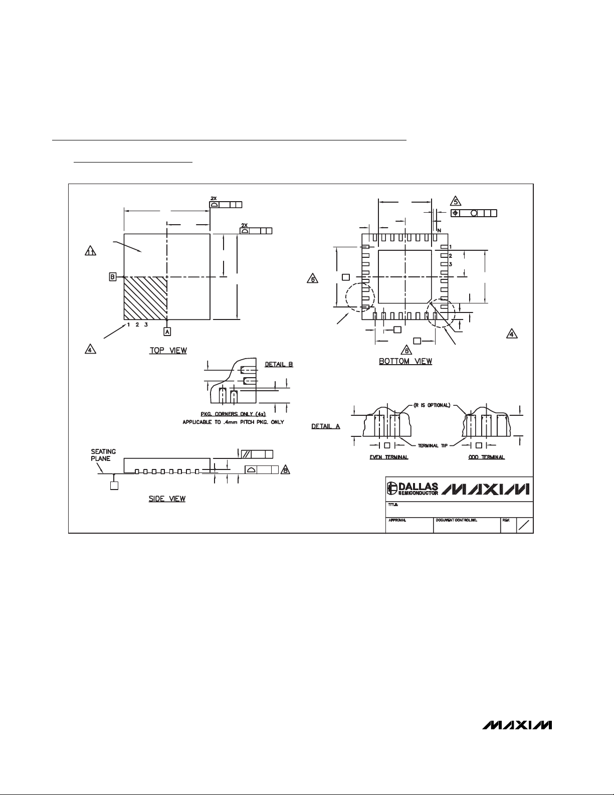
MAX8550/MAX8551
Integrated DDR Power-Supply Solutions for
Desktops, Notebooks, and Graphic Cards
28 ______________________________________________________________________________________
Package Information
(The package drawing(s) in this data sheet may not reflect the most current specifications. For the latest package outline information
go to www.maxim-ic.com/packages
.)
QFN THIN.EPS
D2
(ND-1) X e
e
D
C
PIN # 1
I.D.
(NE-1) X e
E/2
E
0.08 C
0.10 C
A
A1
A3
DETAIL A
0.15
C B
0.15 C A
E2/2
E2
0.10 M C A B
PIN # 1 I.D.
b
0.35x45∞
L
D/2
D2/2
L
C
L
C
e e
L
CC
L
k
k
LL
DETAIL B
L
L1
e
XXXXX
MARKING
F
1
2
21-0140
PACKAGE OUTLINE,
16, 20, 28, 32L THIN QFN, 5x5x0.8mm
-DRAWING NOT TO SCALE-

MAX8550/MAX8551
Integrated DDR Power-Supply Solutions for
Desktops, Notebooks, and Graphic Cards
Maxim cannot assume responsibility for use of any circuitry other than circuitry entirely embodied in a Maxim product. No circuit patent licenses are
implied. Maxim reserves the right to change the circuitry and specifications without notice at any time.
Maxim Integrated Products, 120 San Gabriel Drive, Sunnyvale, CA 94086 408-737-7600 ____________________ 29
© 2004 Maxim Integrated Products Printed USA is a registered trademark of Maxim Integrated Products.
Package Information (continued)
(The package drawing(s) in this data sheet may not reflect the most current specifications. For the latest package outline information
go to www.maxim-ic.com/packages
.)
COMMON DIMENSIONS
3.353.15
T2855-1 3.25 3.353.15 3.25
MAX.
3.20
EXPOSED PAD VARIATIONS
3.00T2055-2 3.10
D2
NOM.MIN.
3.203.00 3.10
MIN.E2NOM. MAX.
NE
ND
PKG.
CODES
1. DIMENSIONING & TOLERANCING CONFORM TO ASME Y14.5M-1994.
2. ALL DIMENSIONS ARE IN MILLIMETERS. ANGLES ARE IN DEGREES.
3. N IS THE TOTAL NUMBER OF TERMINALS.
4. THE TERMINAL #1 IDENTIFIER AND TERMINAL NUMBERING CONVENTION SHALL
CONFORM TO JESD 95-1 SPP-012. DETAILS OF TERMINAL #1 IDENTIFIER ARE
OPTIONAL, BUT MUST BE LOCATED WITHIN THE ZONE INDICATED. THE TERMINAL #1
IDENTIFIER MAY BE EITHER A MOLD OR MARKED FEATURE.
5. DIMENSION b APPLIES TO METALLIZED TERMINAL AND IS MEASURED BETWEEN 0.25 mm AND 0.30 mm
FROM TERMINAL TIP.
6. ND AND NE REFER TO THE NUMBER OF TERMINALS ON EACH D AND E SIDE RESPECTIVELY.
7. DEPOPULATION IS POSSIBLE IN A SYMMETRICAL FASHION.
8. COPLANARITY APPLIES TO THE EXPOSED HEAT SINK SLUG AS WELL AS THE TERMINALS.
9. DRAWING CONFORMS TO JEDEC MO220, EXCEPT EXPOSED PAD DIMENSION FOR T2855-1,
T2855-3 AND T2855-6.
NOTES:
SYMBOL
PKG.
N
L1
e
E
D
b
A3
A
A1
k
10. WARPAGE SHALL NOT EXCEED 0.10 mm.
JEDEC
T1655-1
3.203.00 3.10 3.00 3.10 3.20
0.70 0.800.75
4.90
4.90
0.25
0.250--
4
WHHB
4
16
0.350.30
5.10
5.105.00
0.80 BSC.
5.00
0.05
0.20 REF.
0.02
MIN. MAX.NOM.
16L 5x5
3.10
T3255-2
3.00
3.20
3.00 3.10 3.20
2.70
T2855-2 2.60 2.602.80 2.70 2.80
L
0.30 0.500.40
---
---
WHHC
20
5
5
5.00
5.00
0.30
0.55
0.65 BSC.
0.45
0.25
4.90
4.90
0.25
0.65
--
5.10
5.10
0.35
20L 5x5
0.20 REF.
0.75
0.02
NOM.
0
0.70
MIN.
0.05
0.80
MAX.
---
WHHD-1
28
7
7
5.00
5.00
0.25
0.55
0.50 BSC.
0.45
0.25
4.90
4.90
0.20
0.65
--
5.10
5.10
0.30
28L 5x5
0.20 REF.
0.75
0.02
NOM.
0
0.70
MIN.
0.05
0.80
MAX.
---
WHHD-2
32
8
8
5.00
5.00
0.40
0.50 BSC.
0.30
0.25
4.90
4.90
0.50
--
5.10
5.10
32L 5x5
0.20 REF.
0.75
0.02
NOM.
0
0.70
MIN.
0.05
0.80
MAX.
0.20 0.25 0.30
DOWN
BONDS
ALLOWED
NO
YES3.103.00 3.203.103.00 3.20T2055-3
3.103.00 3.203.103.00 3.20T2055-4
T2855-3 3.15 3.25 3.35 3.15 3.25 3.35
T2855-6 3.15 3.25 3.35 3.15 3.25 3.35
T2855-4 2.60 2.70 2.80 2.60 2.70 2.80
T2855-5 2.60 2.70 2.80 2.60 2.70 2.80
T2855-7 2.60 2.70
2.80
2.60 2.70 2.80
3.203.00 3.10T3255-3 3.203.00 3.10
3.203.00 3.10T3255-4 3.203.00 3.10
NO
NO
NO
NO
NO
NO
NO
NO
YES
YES
YES
YES
3.203.00T1655-2 3.10 3.00 3.10 3.20 YES
NO3.203.103.003.10T1655N-1 3.00 3.20
3.353.15T2055-5 3.25 3.15 3.25 3.35
Y
3.35
3.15T2855N-1 3.25 3.15 3.25 3.35
N
3.35
3.15T2855-8 3.25 3.15 3.25 3.35
Y
3.203.10T3255N-1 3.00
NO
3.203.103.00
L
0.40
0.40
**
**
**
**
**
**
**
**
**
**
**
**
**
**
**
**
**
**
**
SEE COMMON DIMENSIONS TABLE
±0.15
11. MARKING IS FOR PACKAGE ORIENTATION REFERENCE ONLY.
F
2
2
21-0140
PACKAGE OUTLINE,
16, 20, 28, 32L THIN QFN, 5x5x0.8mm
-DRAWING NOT TO SCALE-
12. NUMBER OF LEADS SHOWN ARE FOR REFERENCE ONLY.
 Loading...