

Page 1
General Description
The MAX8543/MAX8544 current-mode, constant-frequency PWM buck controllers operate from a 3V to
13.2V input supply and generate adjustable 0.8V to 0.9
x VINoutput voltages at loads up to 25A. They feature
adjustable switching frequency and synchronization for
noise-sensitive applications.
The MAX8543/MAX8544 can start with (or without) a preexisting bias on the output, without discharging the output. This feature simplifies tracking supply designs for
core and I/O applications and redundant supply designs.
The MAX8543/MAX8544 use the DC resistance of the
output inductor as the current-sense element for lossless, low-cost current sensing. The current-sense
threshold can be set to four discrete levels to accommodate inductors with different DC resistance values.
The MAX8544 features a power-OK monitor and two
MAX8544 controllers that can operate at 180° out-ofphase for dual-output applications.
Applications
Base Stations
Networks and Telecom
Storage
Servers
Features
♦ Prebias Startup/Monotonic
♦ 1% Output Accuracy
♦ Ceramic, Polymer, or Electrolytic Capacitors
♦ 200kHz to 1MHz Adjustable Frequency
♦ 160kHz to 1.2MHz Synchronization
♦ Lossless, Foldback Current Limit
♦ Overvoltage Protection
♦ Enable (On/Off)
♦ Adjustable Soft-Start
♦ MAX8544
Latch-Off/Autorecovery
Power-OK Monitor
Out-of-Phase Clock Output
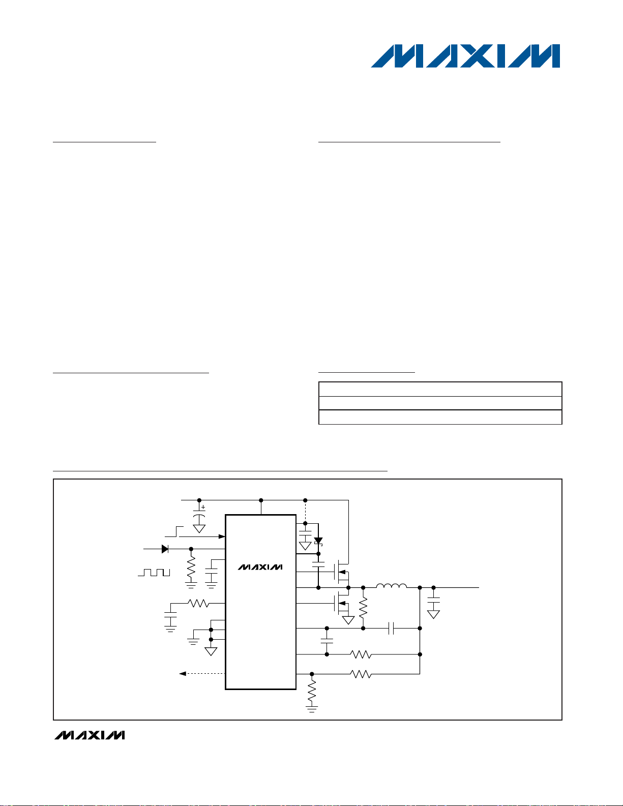
MAX8543/MAX8544
Step-Down Controllers with Prebias Startup,
Lossless Sensing, Synchronization, and OVP
________________________________________________________________ Maxim Integrated Products 1
Ordering Information
MAX8543
ON
OPTIONAL
SYNCHRONIZATION
OFF
BST
VL
V
IN
= 3V
TO 5.5V
COMP
ILIM
FSYNC
EN
SS
PGND
GND
IN
DH
LX
DL
CS+
CS-
FB
INPUT 3V TO 13.2V
OUTPUT
0.8V TO 0.9 x V
IN
UP TO 25A
POK (MAX8544)
Typical Operating Circuit
19-3155; Rev 0; 5/04
For pricing, delivery, and ordering information, please contact Maxim/Dallas Direct! at
1-888-629-4642, or visit Maxim’s website at www.maxim-ic.com.
PART TEMP RANGE
PIN-PACKAGE
MAX8543EEE -40°C to +85°C 16 QSOP
MAX8544EEP -40°C to +85°C 20 QSOP
Pin Configurations appear at end of data sheet.
Page 2
MAX8543/MAX8544
Step-Down Controllers with Prebias Startup,
Lossless Sensing, Synchronization, and OVP
2 _______________________________________________________________________________________
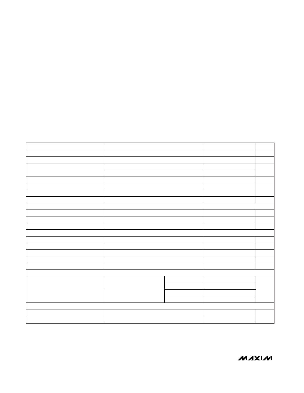
ABSOLUTE MAXIMUM RATINGS
ELECTRICAL CHARACTERISTICS
(VIN= 13.2V, V
BST
- VLX= 5V, TA= 0°C to +85°C, unless otherwise noted. Typical values are at TA= +25°C.)
Stresses beyond those listed under “Absolute Maximum Ratings” may cause permanent damage to the device. These are stress ratings only, and functional
operation of the device at these or any other conditions beyond those indicated in the operational sections of the specifications is not implied. Exposure to
absolute maximum rating conditions for extended periods may affect device reliability.
IN, EN, CS+, CS- to GND .......................................-0.3V to +14V
BST, DH to LX ..........................................................-0.3V to +6V
BST to GND ............................................................-0.3V to +20V
DL, COMP, ILIM2, SS, SYNCO,
FSYNC to GND .......................................-0.3V to (V
VL
+ 0.3V)
VL, FB, POK, ILIM1, ILIM, MODE to GND ................-0.3V to +6V
PGND to GND .......................................................-0.3V to +0.3V
Continuous Power Dissipation (T
A
= +70°C)
16-Pin QSOP (derate 8.3mW/°C above +70°C) .......666.7mW
20-Pin QSOP (derate 9.1mW/°C above +70°C) .......727.3mW
Operating Temperature Range ...........................-40°C to +85°C
Junction Temperature......................................................+150°C
Storage Temperature Range .............................-65°C to +150°C
Lead Temperature (soldering, 10s) .................................+300°C
PARAMETER CONDITIONS
UNITS
Operating Input Voltage Range VL connected to IN for V
IN
< 5.5V 3.0
V
Quiescent Supply Current V
FB
= 0.9V, no switching 2 3 mA
10
Shutdown Supply Current
EN = GND, VL = IN, MODE = GND 20
µA
VL Undervoltage-Lockout Trip Level V
VL
rising, typical hysteresis is 80mV
2.7
V
Output Voltage Adjust Range (V
OUT
) (Note 1) 0.8 V
VL Output Voltage 5.5V < V
IN
< 13.2V, 1mA < IVL < 75mA 4.5 5 5.5 V
VL Output Current 75 mA
VOLTAGE REFERENCE
SS Shutdown Resistance From SS to GND, V
EN
= 0V 20
Ω
SS Soft-Start Current V
REF
= 0.625V 14 24 34 µA
Soft-Start Ramp Time Output from 0% to 100%, C
REF
= 0.01µF to 1µF 33
ms/µF
ERROR AMPLIFIER
FB Regulation Voltage
0.8
V
Transconductance 70
µS
COMP Shutdown Resistance From COMP to GND, V
EN
= 0V 20
Ω
FB Input Leakage Current V
FB
= 0.9V 5
nA
FB Input Common-Mode Range
V
CURRENT-SENSE AMPLIFIER
V
ILIM1
= 0V 8.8 11
4.8 6 7.2
3.2 4 4.8
Voltage Gain V
OUT
= 0 to 13V
V
ILIM1
= V
VL
2.4 3 3.6
V / V
CURRENT LIMIT
ILIM2 Output Current (MAX8544 Only) R
ILIM2
= 50kΩ to 200kΩ 4.5 5 5.5 µA
ILIM1 Input Current V
ILIM1
= 0V or V
VL
-1 +1 µA
MIN TYP MAX
13.2
EN = GND, MODE = GND, IN not connected to VL
2.52
0.792
-0.1
110 160
V
V
ILIM1
ILIM1
= (1/3)V
= (2/3)V
VL
VL
2.88
100
0.808
100
100
+0.9
13.2
Page 3
MAX8543/MAX8544
Step-Down Controllers with Prebias Startup,
Lossless Sensing, Synchronization, and OVP
_______________________________________________________________________________________ 3
ELECTRICAL CHARACTERISTICS (continued)
(VIN= 13.2V, V
BST
- VLX= 5V, TA= 0°C to +85°C, unless otherwise noted. Typical values are at TA= +25°C.)
PARAMETER CONDITIONS
MIN
TYP
MAX
UNITS
V
CS+
- V
CS-, VILIM1
= 0V
50
V
CS+
- V
CS-, VILIM1
= (1/3)V
VL
85
V
CS+
- V
CS-
, V
ILIM1
= (2/3)V
VL
V
CS+
- V
CS-
, V
ILIM1
= V
VL
V
LX
- V
PGND
, R
ILIM2
= 50kΩ (MAX8544 only)
-50
V
LX
- V
PGND
, R
ILIM2
= 200kΩ (MAX8544 only)
V
LX
- V
PGND
, VFB = 0.8V (MAX8543 only)
Current-Limit Threshold
V
LX
- V
PGND
, VFB = 0V (MAX8543 only) -20 -30 -40
mV
Negative Current-Limit Threshold % of positive-direction current limit V
LX
- V
PGND
-25 -50 -85 %
CS+, CS- Input Current V
CS+
= V
CS-
= 0 or 5V -40
µA
CS+, CS- Input Common-Mode Range 0
V
OSCILLATOR
R
FSYNC
= 18.2kΩ
Switching Frequency
R
FSYNC
= 158kΩ
kHz
Minimum Off-Time Measured at DH
ns
Minimum On-Time Measured at DH 90
ns
FSYNC Synchronization Range
kHz
FSYNC Input High Pulse Width
ns
FSYNC Input Low Pulse Width
ns
FSYNC Rise/Fall Time
ns
SYNCO Phase Shift from DH Rising
R
FSYNC
= 18.2kΩ, free-running mode,
at maximum duty cycle
Degrees
SYNCO Output Low Level I
SYNCO
= 5mA 0.4 V
SYNCO Output High Level I
SYNCO
= 5mA
V
MOSFET DRIVERS
(V
BST
- VLX) = 5V 1 2.5
DH On-Resistance, High State
(V
BST
- VLX) = 3V 1.2
Ω
(V
BST
- VLX) = 5V 1 2.5
DH On-Resistance, Low State
(V
BST
- VLX) = 3V 1.2
Ω
V
VL
= 5V 1 2.5
DL On-Resistance, High State
V
VL
= 3V 1.2
Ω
V
VL
= 5V 0.6 1.7
DL On-Resistance, Low State
V
VL
= 3V 0.8
Ω
Low-side off to high-side on 55
Break-Before-Make Dead Time
High-side off to low-side on 40
ns
LX, BST, IN Leakage Current V
BST
= 18.7V, VLX = 13.2V, VIN = 13.2V 5 µA
THERMAL PROTECTION
Thermal Shutdown Rising temperature
°C
Thermal-Shutdown Hysteresis 15 °C
38.5
56.5
100 115
127.5 150 172.5
170 200 230
-42.5
-57.5
-160 -200 -240
-110 -130 -150
800 1000 1200
200
150 220 270
160
100
100
165 180 195
V
- 1V
VL
+40
13.2
145
1200
100
+160
Page 4
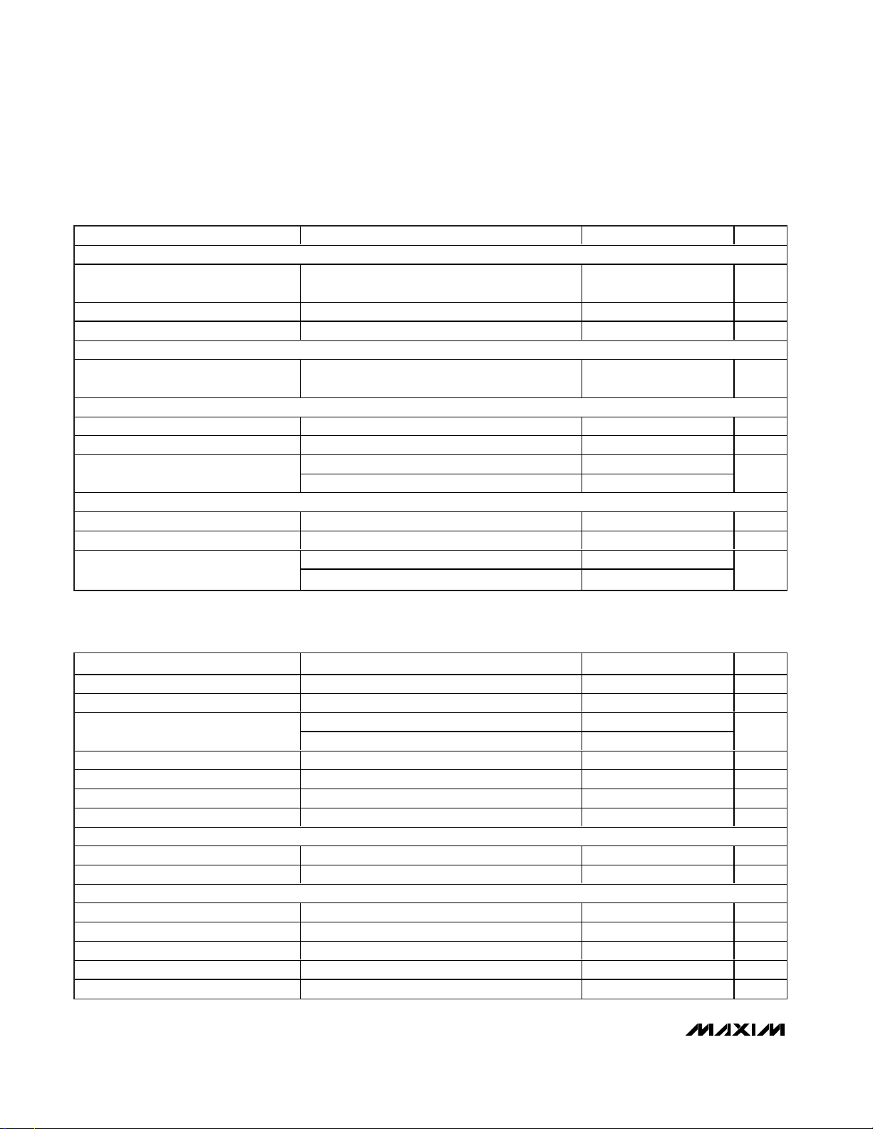
MAX8543/MAX8544
Step-Down Controllers with Prebias Startup,
Lossless Sensing, Synchronization, and OVP
4 _______________________________________________________________________________________
ELECTRICAL CHARACTERISTICS (continued)
(VIN= 13.2V, V
BST
- VLX= 5V, TA= 0°C to +85°C, unless otherwise noted. Typical values are at TA= +25°C.)
PARAMETER CONDITIONS
MIN
TYP
MAX
UNITS
POK
Power-OK Threshold
V
FB
rising, percent of V
OUT
,
typical hysteresis is 3%
88 91 94 %
POK Output Voltage, Low V
FB
= 0.6V, I
POK
= 2mA 25
mV
POK Leakage Current, High V
POK
= 5.5V
1 µA
OVERVOLTAGE PROTECTION (OVP)
Output Overvoltage Fault-Trip level
Rising edge compared to regulation set point;
triggers after one or two clock cycles
%
MODE CONTROL
MODE Logic-Level Low 3V ≤ V
VL
≤ 5.5V 0.4 V
MODE Logic-Level High 3V ≤ V
VL
≤ 5.5V
1.8 V
V
MODE
= 0V -1 +1
MODE Input Current
MODE = VL 5 10
µA
SHUTDOWN CONTROL
EN Logic-Level Low 3V ≤ V
VL
≤ 5.5V
V
EN Logic-Level High 3V ≤ V
VL
≤ 5.5V 2 V
V
EN
= 0 or 5.5V -1 +4
EN Input Current
V
EN
= 13.2V 1.5 6
µA
ELECTRICAL CHARACTERISTICS
(VIN= 13.2V, V
BST
- VLX= 5V, TA= -40°C to +85°C, unless otherwise noted.) (Note 2)
PARAMETER CONDITIONS
UNITS
Operating Input Voltage Range VL connected to IN for V
IN
< 5.5V 3.0
V
Quiescent Supply Current V
FB
= 0.9V, no switching 3 mA
10
Shutdown Supply Current
EN = GND, VL = IN, MODE = GND 20
µA
VL Undervoltage-Lockout Trip Level V
VL
rising, typical hysteresis is 80mV
V
Output Voltage Adjust Range (V
OUT
) (Note 1) 0.8 V
VL Output Voltage 5.5V < V
IN
< 13.2V, 1mA < IVL < 75mA 4.5 5.5 V
VL Output Current 75 mA
VOLTAGE REFERENCE
SS Shutdown Resistance From SS to GND, V
EN
= 0V 100 Ω
SS Soft-Start Current V
REF
= 0.625V 14 34 µA
ERROR AMPLIFIER
FB Regulation Voltage
V
Transconductance 70 160 µS
COMP Shutdown Resistance From COMP to GND, V
EN
= 0V 100 Ω
FB Input Leakage Current V
FB
= 0.9V 100 nA
FB Input Common-Mode Range
V
0.001
+110 +115 +120
200
0.45
MIN
EN = GND, MODE = GND, IN not connected to VL
2.52
0.788
-0.1
MAX
13.2
2.88
0.808
+0.9
Page 5
MAX8543/MAX8544
Step-Down Controllers with Prebias Startup,
Lossless Sensing, Synchronization, and OVP
_______________________________________________________________________________________ 5
ELECTRICAL CHARACTERISTICS (continued)
(VIN= 13.2V, V
BST
- VLX= 5V, TA= -40°C to +85°C, unless otherwise noted.) (Note 2)
PARAMETER CONDITIONS
UNITS
CURRENT-SENSE AMPLIFIER
V
ILIM1
= 0V 8.8
4.8 7.2
3.2 4.8
Voltage Gain V
OUT
= 0 to 13V
V
ILIM1
= V
VL
2.4 3.6
V / V
CURRENT LIMIT
ILIM2 Output Current (MAX8544 Only) R
ILIM2
= 50kΩ to 200kΩ 4.2 5.5 µA
ILIM1 Input Current V
ILIM1
= 0V or V
VL
-1 +1 µA
V
CS+
- V
CS-, VILIM1
= 0V
V
CS+
- V
CS-, VILIM1
= (1/3)V
VL
85 115
V
CS+
- V
CS-
, V
ILIM1
= (2/3)V
VL
V
CS+
- V
CS-, VILIM1
= V
VL
230
V
LX
- V
PGND
, R
ILIM2
= 50kΩ (MAX8544 only) -40 -60
V
LX
- V
PGND
, R
ILIM2
= 200kΩ (MAX8544 only)
V
LX
- V
PGND
, VFB = 0.8V (MAX8543 only)
Current-Limit Threshold
V
LX
- V
PGND
, VFB = 0V (MAX8543 only) -20 -40
mV
Negative Current-Limit Threshold % of positive-direction current limit V
LX
- V
PGND
-25 -85 %
CS+, CS- Input Current V
CS+
= V
CS-
= 0V or 5V -40
µA
CS+, CS- Input Common-Mode Range 0
V
OSCILLATOR
Switching Frequency R
FSYNC
= 18.2kΩ
kHz
Minimum Off-Time Measured at DH
270 ns
Minimum On-Time Measured at DH 140 ns
FSYNC Synchronization Range
kHz
FSYNC Input High Pulse Width
ns
FSYNC Input Low Pulse Width
ns
FSYNC Rise/Fall Time 100 ns
SYNCO Phase Shift from DH Rising R
FSYNC
= 18.2kΩ
195
Degrees
SYNCO Output Low Level I
SYNCO
= 5mA 0.4 V
SYNCO Output High Level I
SYNCO
= 5mA
V
MOSFET DRIVERS
DH On-Resistance, High State (V
BST
- VLX) = 5V 2.5 Ω
DH On-Resistance, Low State (V
BST
- VLX) = 5V 2.5 Ω
DL On-Resistance, High State V
VL
= 5V 2.5 Ω
DL On-Resistance, Low State V
VL
= 5V 1.7 Ω
LX, BST, IN Leakage Current V
BST
= 18.7V, VLX = 13.2V, VIN = 13.2V 5 µA
V
V
ILIM1
ILIM1
= (1/3)V
= (2/3)V
MIN
VL
VL
38.5
127.5
170
-160
-110
800
150
160
100
100
165
V
- 1V
VL
MAX
13.2
56.5
172.5
-240
-150
+40
13.2
1200
1200
Page 6
MAX8543/MAX8544
Step-Down Controllers with Prebias Startup,
Lossless Sensing, Synchronization, and OVP
6 _______________________________________________________________________________________
ELECTRICAL CHARACTERISTICS (continued)
(VIN= 13.2V, V
BST
- VLX= 5V, TA= -40°C to +85°C, unless otherwise noted.) (Note 2)
PARAMETER CONDITIONS
UNITS
POK
Power-OK Threshold
V
FB
rising, percent of V
OUT
,
typical hysteresis is 3%
88 94 %
POK Output Voltage, Low V
FB
= 0.6V, I
POK
= 2mA 200 mV
POK Leakage Current, High V
POK
= 5.5V 1 µA
OVERVOLTAGE PROTECTION (OVP)
Output Overvoltage Fault-Trip level
Rising edge compared to regulation set point;
triggers after one or two clock cycles
%
MODE CONTROL
MODE Logic-Level Low 3V ≤ V
VL
≤ 5.5V
0.4 V
MODE Logic-Level High 3V ≤ V
VL
≤ 5.5V
1.8 V
V
MODE
= 0V -1 +1
MODE Input Current
MODE = VL 10
µA
SHUTDOWN CONTROL
EN Logic-Level Low 3V ≤ V
VL
≤ 5.5V
V
EN Logic-Level High 3V ≤ V
VL
≤ 5.5V
2 V
V
EN
= 0V or 5.5V -1 +4
EN Input Current
V
EN
= 13.2V 6
µA
Note 1: Maximum output voltage is limited by maximum duty cycle and external components.
Note 2: Specifications to -40°C are guaranteed by design and not production tested.
MIN
MAX
+110
+120
0.45
Page 7
MAX8543/MAX8544
Step-Down Controllers with Prebias Startup,
Lossless Sensing, Synchronization, and OVP
_______________________________________________________________________________________ 7
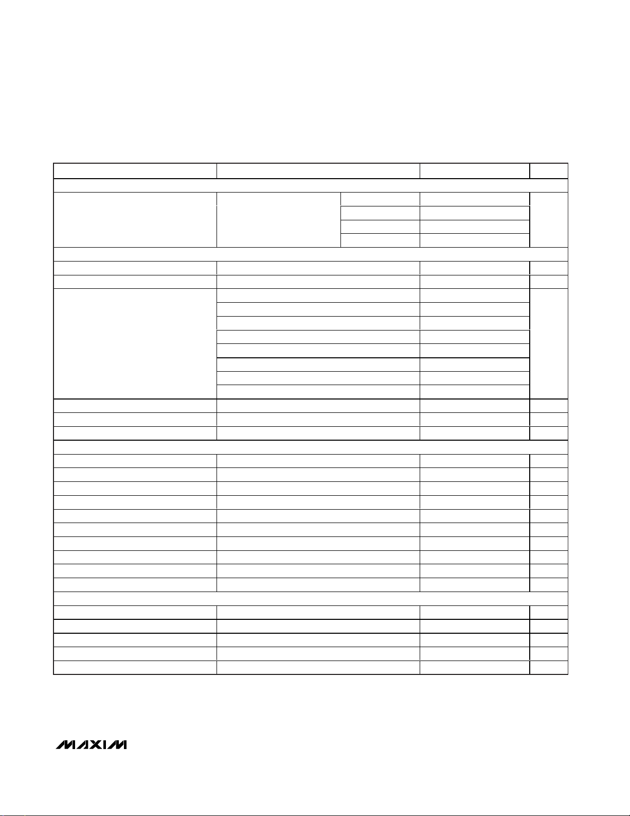
EFFICIENCY vs. LOAD CURRENT
WITH 12V INPUT
MAX8543 toc01
LOAD CURRENT (A)
EFFICIENCY (%)
101
10
20
30
40
50
60
70
80
90
100
0
0.1 100
V
OUT
= 3.3V
V
OUT
= 2.5V
V
OUT
= 1.8V
fS = 600kHz
EFFICIENCY vs. LOAD CURRENT
WITH 3.3V INPUT
MAX8543 toc02
LOAD CURRENT (A)
EFFICIENCY (%)
101
10
20
30
40
50
60
70
80
90
100
0
0.1 100
V
OUT
= 2.5V
V
OUT
= 1.8V
fS = 500kHz
V
OUT
= 1.5V
LOAD REGULATION WITH 12V INPUT
MAX8543 toc03
LOAD CURRENT (A)
OUTPUT VOLTAGE (V)
12963
2.46
2.47
2.48
2.49
2.50
2.51
2.52
2.53
2.54
2.55
2.45
015
LINE REGULATION WITH 12V INPUT
AND 2.5V OUTPUT
MAX8543 toc04
INPUT VOLTAGE (V)
OUTPUT VOLTAGE (V)
12.612.011.4
2.492
2.494
2.496
2.498
2.500
2.502
2.504
2.506
2.508
2.510
2.490
10.8 13.2
NO LOAD
15A LOAD
LINE REGULATION
3.0V TO 3.6V INPUT
MAX8543 toc05
INPUT VOLTAGE (V)
OUTPUT VOLTAGE (V)
3.53.43.33.23.1
2.44
2.46
2.48
2.50
2.52
2.54
2.42
3.0 3.6
NO LOAD
15A LOAD
f
S
= 350kHz
15A LOAD
f
S
= 500kHz
OSCILLATOR FREQUENCY
vs. INPUT VOLTAGE
MAX8543 toc06
INPUT VOLTAGE (V)
OSCILLATOR FREQUENCY (kHz)
5.04.54.03.5
420
440
460
480
500
520
540
560
580
600
400
3.0 5.5
TA = +85°C
TA = +25°C
TA = -40°C
R6 = 53.6k
Ω
OSCILLATOR FREQUENCY
vs. INPUT VOLTAGE
MAX8543 toc07
INPUT VOLTAGE (V)
OSCILLATOR FREQUENCY (kHz)
11.59.57.5
520
540
560
580
600
620
640
660
680
700
500
5.5 13.5
R6 = 42.2kΩ
TA = +85°C
TA = -40°C
TA = +25°C
Typical Operating Characteristics
(TA = +25°C, unless otherwise noted.)
Page 8
MAX8543/MAX8544
Step-Down Controllers with Prebias Startup,
Lossless Sensing, Synchronization, and OVP
8 _______________________________________________________________________________________
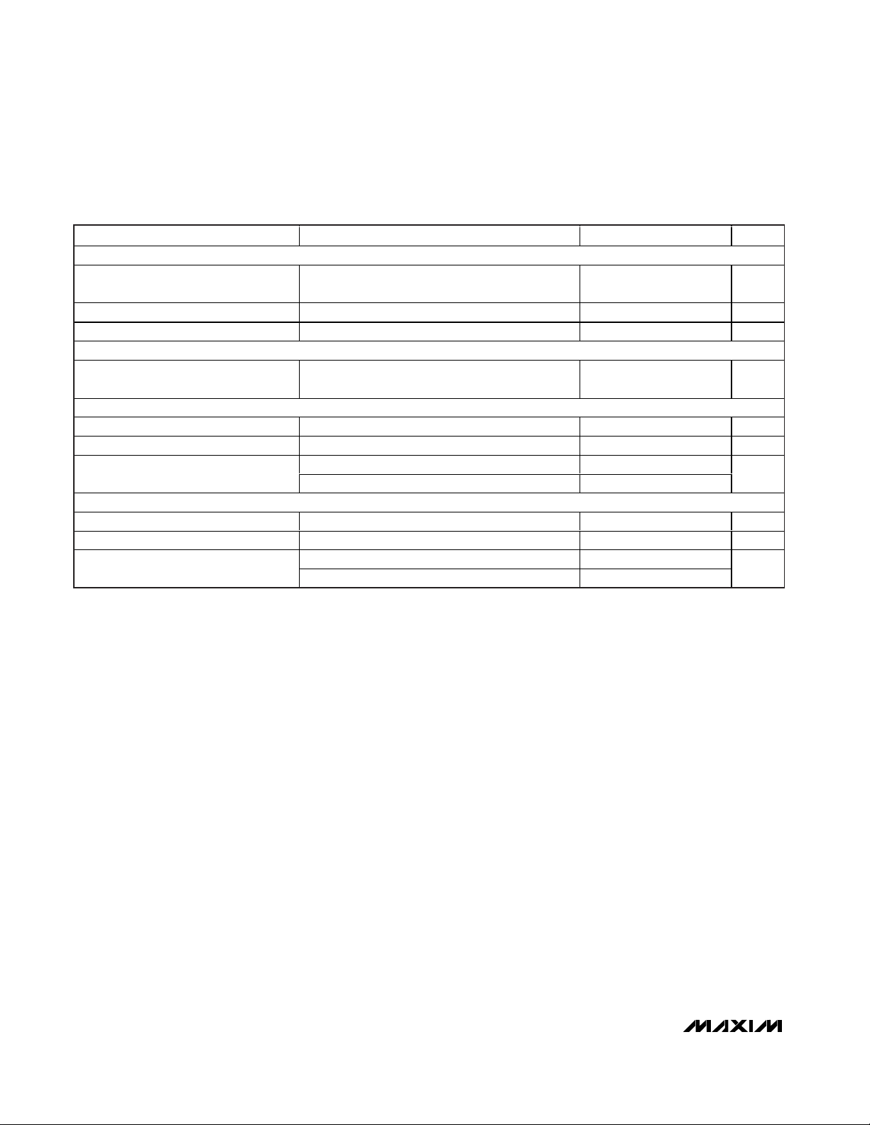
Typical Operating Characteristics (continued)
(TA = +25°C, unless otherwise noted.)
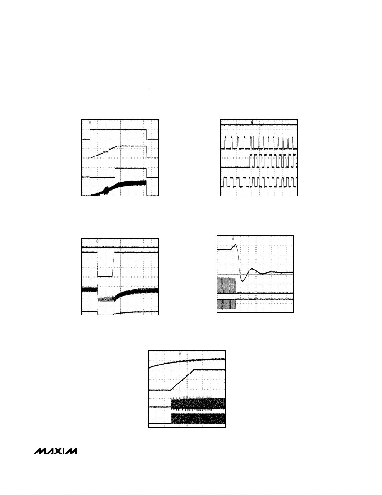
MAX8544 STEP-LOAD RESPONSE
7.5A TO 15A TO 7.5A (5A/μs)
MAX8543 toc08
V
OUT
I
OUT
50mV/div
AC-COUPLED
0
5A/div
10μs/div
MAX8544 STEP-LOAD RESPONSE
1.5A TO 15A TO 1.5A (5A/μs)
MAX8543 toc09
V
OUT
I
OUT
100mV/div
AC-COUPLED
0
5A/div
10μs/div
MAX8544 POWER-UP WAVEFORMS
MAX8543 toc10
V
IN
V
POK
5V/div
0
10A/div
2ms/div
V
OUT
I
L
2V/div
5V/div
MAX8544 POWER-DOWN WAVEFORMS
MAX8543 toc11
V
IN
V
POK
5V/div
0
10A/div
2ms/div
V
OUT
I
L
2V/div
2V/div
MAX8543 POWER-UP WAVEFORMS
MAX8543 toc12
V
IN
2V/div
0
10A/div
2ms/div
V
OUT
I
L
1V/div
MAX8543 POWER-DOWN WAVEFORMS
MAX8543 toc13
V
IN
2V/div
0
10A/div
2ms/div
V
OUT
I
L
1V/div
Page 9
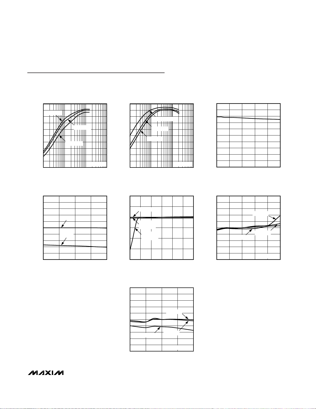
MAX8543/MAX8544
Step-Down Controllers with Prebias Startup,
Lossless Sensing, Synchronization, and OVP
_______________________________________________________________________________________ 9
MAX8544 ENABLE WAVEFORMS
MAX8543 toc14
V
EN
5V/div
0
10A/div
2ms/div
V
OUT
I
L
2V/div
V
POK
5V/div
FSYNC AND SYNCO WAVEFORMS
MAX8543 toc15
V
OUT
1V/div
5V/div
2μs/div
V
LX
V
SYNCO
10V/div
V
FSYNC
5V/div
SHORT CIRCUIT AND RECOVERY
MAX8543 toc16
V
IN
10V/div
12V
0
1ms/div
V
OUT
I
IN
1V/div
I
L
10A/div
0
10A/div
OVERVOLTAGE PROTECTION
WITH 15A LOAD
MAX8543 toc17
V
OUT
5V/div
40μs/div
V
DH
V
DL
1V/div
10V/div
0V
0V
5V
5V
PREBIASED STARTUP
(OUTPUT PREBIASED AT 1.5V)
MAX8543 toc18
V
IN
5V/div
1ms/div
V
LX
V
DL
2.5V
10V/div
V
OUT
5V/div
500mV/div
1.5V
Typical Operating Characteristics (continued)
(TA = +25°C, unless otherwise noted.)
Page 10

MAX8543/MAX8544
Step-Down Controllers with Prebias Startup,
Lossless Sensing, Synchronization, and OVP
10 ______________________________________________________________________________________
Pin Description
PIN
MAX8543
NAME FUNCTION
1 2 GND Ground. Connect to the analog ground plane.
23SS
Soft-Start. Connect a 0.1µF to 1µF ceramic capacitor from SS to GND. This capacitor
sets the soft-start period during startup. See the Startup and Soft-Start section. SS is
internally pulled to GND in shutdown.
3 4 COMP
Compensation. Connect to an external RC network to compensate the feedback loop.
See the Compensation Design section. COMP is internally pulled to GND in shutdown.
45FB
Output Feedback. Connect to the center of a voltage-divider connected between OUT
and GND to set the output voltage. The FB threshold voltage is 0.8V.
56EN
Enable. Drive EN logic high to enable the output, or drive logic low for shutdown.
Connect EN to IN for always-on operation.
6 7 CS- Negative Differential Current-Sensing Input
7 8 CS+ Positive Differential Current-Sensing Input
— 9 ILIM1
8 — ILIM
Digital Programmable Current-Limit Input for Inductor Current Sensing (V
CS+
- V
CS-
).
See Table 3.
9 12 PGND
Power Ground. Connect to the power ground plane and to the source of the low-side
external MOSFETs. Connect PGND to GND at a single point.
10 13 DL
Low-Side MOSFET Gate-Driver Output. Connect to the gate of the low-side external
MOSFETs. DL is pulled low in shutdown.
11 14 VL
Internal 5V Linear-Regulator Output. Connect a 1µF to 10µF ceramic capacitor from
VL to PGND. Connect VL to IN for VIN less than 5.5V. VL provides power for bias and
gate drive.
12 15 IN
Input Supply Voltage. IN is the input to the internal linear regulator. Connect VL to IN for
V
IN
less than 5.5V.
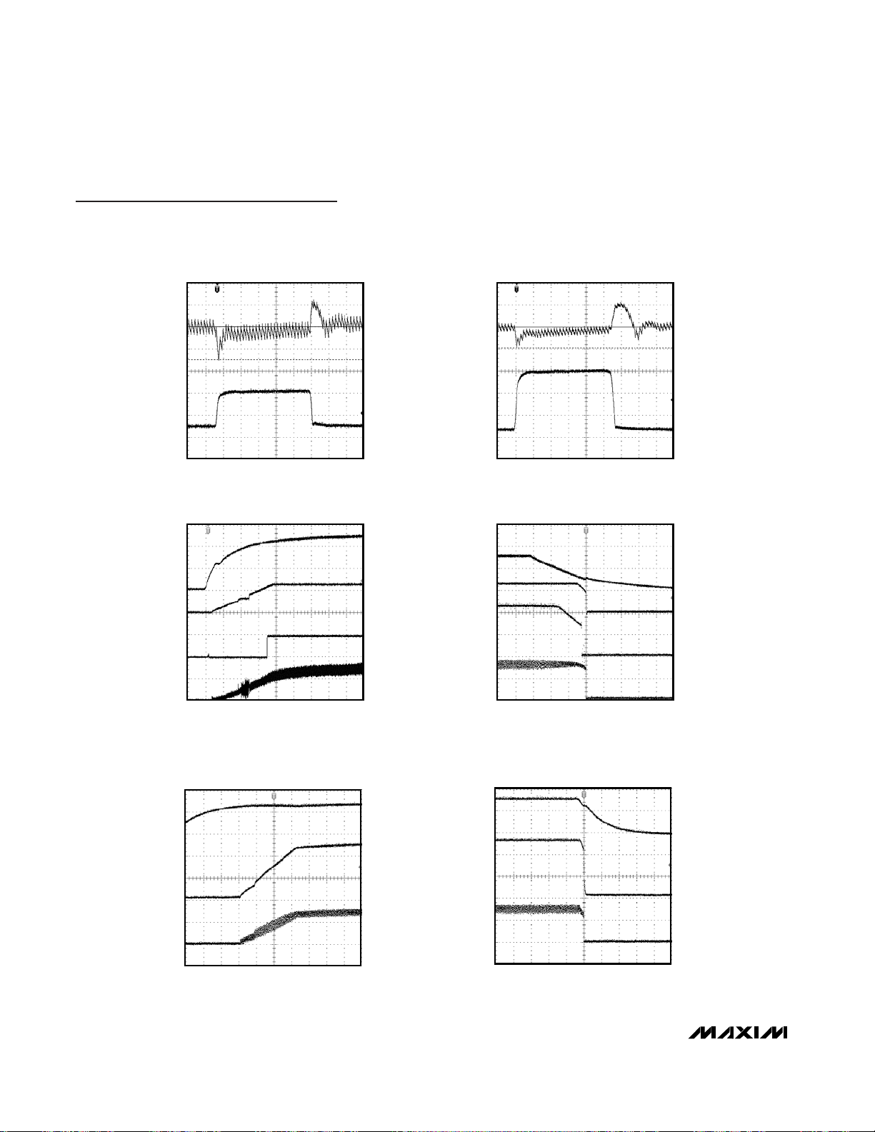
Typical Operating Characteristics (continued)
(TA = +25°C, unless otherwise noted.)
BODE PLOT, 600kHz, 15A LOAD
SWEEP TIME
10.000s
MAX8543 toc19
BODE PLOT, 600kHz, NO LOAD
SWEEP TIME
10.000s
MAX8543 toc20
0dB
10dB/div
1kHz 1MHz100kHz10kHz
°
90
30°/div
MAX8544
0dB
10dB/div
1kHz 1MHz100kHz10kHz
°
90
30°/div
Page 11

MAX8543/MAX8544
Step-Down Controllers with Prebias Startup,
Lossless Sensing, Synchronization, and OVP
______________________________________________________________________________________ 11
Pin Description (continued)
PIN
MAX8543
NAME FUNCTION
13 16 LX Inductor Connection
14 17 DH
High-Side MOSFET Gate-Driver Output. Connect DH to the gate of the high-side
external MOSFETs. DH is pulled low in shutdown.
15 18 BST
Boost Capacitor Connection. Connect a 0.1µF or larger ceramic capacitor from BST to
LX. BST provides power for the high-side MOSFET gate drive.
16 19 FSYNC
Frequency Set and Synchronization. Connect a resistor from FSYNC to GND to set the
switching frequency or drive with a clock signal to synchronize between 160kHz and
1.2MHz. See the Switching Frequency and Synchronization section.
— 1 ILIM2
Analog Programmable Current-Limit Input for Low-Side MOSFET (V
LX
- V
PGND
).
Connect a resistor from ILIM2 to ground to set the overcurrent threshold. See the
Setting the Current Limits section.
— 10 MODE
Current-Limit Operating-Mode Selection. Connect MODE to VL for latch-off current limit
or connect to GND for automatic-recovery current limit with the MAX8544. The MAX8543
always uses automatic-recovery current limit.
—11POK
Power-OK. POK is an open-drain output that is high impedance when the output is
above 91% of its nominal regulation voltage. POK is pulled low when the output is out
of regulation and when the part is in shutdown. To use POK as a logic-level signal,
connect a pullup resistor from POK to the logic supply.
— 20 SYNCO
Synchronization Output. Provides a clock output that is 180° out of phase with the rising
edge of DH for out-of-phase synchronization of another MAX8544.
MAX8544
Page 12

MAX8543/MAX8544
Step-Down Controllers with Prebias Startup,
Lossless Sensing, Synchronization, and OVP
12 ______________________________________________________________________________________
MAX8544EEP
SS
COMP
MODE
SYNCO
POK
VL
GND
VL
EN
LX
ILIM2
CS-
CS+
PGND
DL
BST
DH
IN
ILIM1
FSYNC
FB
9
19
6
2
3
4
5
10
1
11
20
7
8
12
13
18
D1
C1
C2
C4A C4B C4C
VL
VL
17
16
14
15
C3
C6A C6B
SYNC OUT
R6
R3
R1
R7
R9
POK
R2
R8
D2
C5
C9
N3
N4
L1
V
OUT
= 2.5V
UP TO 15A
V
IN
= (10.8V TO 13.2V)
N2
N1
C7
C8
ON
OFF
SYNC IN
R4
R5
C11
C10
C12
Figure 1. Typical Applications Circuit with 12V (±10%) Input, 2.5V Output at Up to 15A, and 600kHz Switching Frequency
Page 13

MAX8543/MAX8544
Step-Down Controllers with Prebias Startup,
Lossless Sensing, Synchronization, and OVP
______________________________________________________________________________________ 13
Table 1. Suggested Components for Figure 1
DESIGNATION QTY DESCRIPTION
C1 1
1µF ±20%, 16V X5R ceramic capacitor (0603)
Panasonic ECJ1VB1C105M or equivalent
C2 1
10µF ±20%, 6.3V X5R ceramic capacitor (0805)
Panasonic ECJ2FB0J106M or Taiyo Yuden JMK212BJ106MG
C3 1
0.1µF ±10%, 50V X7R ceramic capacitor (0603)
TDK C1608X7R1H104KT or equivalent
C4A, C4B, C4C 2
10µF ±20%, 16V X5R ceramic capacitors (1206)
Panasonic ECJ3YB1C106M or equivalent
C5 1
0.22µF ±10%, 10V X7R ceramic capacitor (0603)
Taiyo Yuden LMK107BJ224KA or equivalent
C6A, C6B 2
180µF, 4V aluminum poly SPCAPs
Panasonic EEFUE0G181XR
C7 1 10pF, 50V C0G ceramic capacitor (0603)
C8 1 220pF ±10%, 50V X7R ceramic capacitor (0603)
C9, C10 2 0.47µF ±10% X7R ceramic capacitors (0603)
C11 1 100pF, 50V C0G ceramic capacitor (0603)
C12 1
470µF ±20%, 16V aluminum electrolytic capacitor
Rubycon 16MBZ470M
D1 1
100mA, 30V Schottky diode (SOT-323)
Central CMSSH-3
D2 1
250mA, 100V switching diode (SOT23)
Central CMPD914
L1 1
0.82µH, 33A, 1.6mΩ inductor
Vishay IHLP-5050FD-01 0.82µH
N1, N2 2
N-channel MOSFETs
IRF IRF7821
N3, N4 2
N-channel MOSFETs
IRF IRF7832
R1 1 17.4kΩ ±1% resistor (0603)
R2 1 8.06kΩ ±1% resistor (0603)
R3 1 220kΩ ±5% resistor (0603)
R4, R5 2 1.3kΩ ±5% resistors (0603)
R6 1 42.2kΩ ±1% resistor (0603)
R7 1 90.9kΩ ±1% resistor (0603)
R8 1 9.31kΩ ±1% resistor (0603)
R9 1 100kΩ ±5% resistor (0603)
Page 14

MAX8543/MAX8544
Step-Down Controllers with Prebias Startup,
Lossless Sensing, Synchronization, and OVP
14 ______________________________________________________________________________________
MAX8543
SS
COMP
CS-
GND
VL
EN
LX
FB
CS+
PGND
DL
BST
DH
IN
ILIM
FSYNC
8
16
5
1
2
3
4
6
7
9
10
15
D1
C1
C2
C4A C4B C4D
IN
14
13
11
12
C3
C6A C6B
R6
R3
R1
R2
D2
C5
C9
R4
R5
N3
N4
L1
V
OUT
= 2.5V
UP TO 15A
V
IN
= (3V TO 3.6V)
N2
N1
C7
C8
C4C
ON
OFF
SYNC IN
C12
C11
C10
Figure 2. Typical Applications Circuit with 3.3V (±10%) Input, 2.5V Output at Up to 15A, and 500kHz Switching Frequency
Page 15

MAX8543/MAX8544
Step-Down Controllers with Prebias Startup,
Lossless Sensing, Synchronization, and OVP
______________________________________________________________________________________ 15
Table 2. Suggested Components for Figure 2
DESIGNATION QTY DESCRIPTION
C1 1
1µF ±10%, 16V X5R ceramic capacitor (0603)
Panasonic ECJ1VB1C105K or equivalent
C2 1
10µF ±20%, 6.3V X5R ceramic capacitor (0805)
Panasonic ECJ2FB0J106M or Taiyo Yuden JMK212BJ106MG
C3 1
0.1µF ±10%, 50V X7R ceramic capacitor (0603)
TDK C1608X7R1H104KT or equivalent
C4A, C4B, C4C,
C4D
4
10µF ±20%, 16V X5R ceramic capacitors (1206)
Panasonic ECJ3YB1C106M or equivalent
C5 1
0.22µF ±10%, 10V X7R ceramic capacitor (0603)
Taiyo Yuden LMK107BJ224KA or equivalent
C6A, C6B 2
180µF, 4V, 10mΩ aluminum poly SPCAPs
Panasonic EEFUE0G181XR
C7 1 12pF, 50V C0G ceramic capacitor (0603)
C8 1 220pF ±10%, 50V X7R ceramic capacitor (0603)
C9, C10 2 0.47µF ±10% X7R ceramic capacitors (0603)
C11 1 100pF, 50V C0G ceramic capacitor (0603)
C12 1
470µF ±20%, 6.3V POSCAP
Sanyo 6PB470M
D1 1
100mA, 30V Schottky diode (SOT-323)
Central CMSSH-3
D2 1
250mA, 100V switching diode (SOT23)
Central CMPD914
L1 1
0.33µH, 16A, 2mΩ inductor (13 x 10 x 6.35)
Coilcraft DO3316P-331HC
N1, N2 2
N-channel MOSFETs
Vishay Si4866DY
N3, N4 2
N-channel MOSFETs
Vishay Si4866DY
R1 1 17.4kΩ ±1% resistor (0603)
R2 1 8.06kΩ ±1% resistor (0603)
R3 1 150kΩ ±5% resistor (0603)
R4, R5 2 680Ω ±5% resistors (0603)
R6 1 53.6kΩ ±1% resistor (0603)
Page 16

MAX8543/MAX8544
Step-Down Controllers with Prebias Startup,
Lossless Sensing, Synchronization, and OVP
16 ______________________________________________________________________________________
Detailed Description
DC-DC Converter Control Architecture
The MAX8543/MAX8544 step-down controllers use a
PWM, current-mode control scheme. An internal
transconductance amplifier establishes an integrated
error voltage. The heart of the PWM controller is an
open-loop comparator that compares the integrated
voltage-feedback signal against the amplified currentsense signal plus the slope-compensation ramp, which
are summed into the main PWM comparator to preserve inner-loop stability and eliminate inductor staircasing. At each rising edge of the internal clock, the
high-side MOSFET turns on until the PWM comparator
trips or the maximum duty cycle is reached or the peak
current limit is reached. During this on-time, current
ramps up through the inductor, storing energy in a
magnetic field and sourcing current to the output. The
current-mode feedback system regulates the peak
inductor current as a function of the output-voltageerror signal. The circuit acts as a switch-mode
transconductance amplifier and pushes the output LC
filter pole normally found in a voltage-mode PWM to a
higher frequency.
During the second half of the cycle, the high-side
MOSFET turns off and the low-side MOSFET turns on.
The inductor releases the stored energy as the current
ramps down, providing current to the output. The output capacitor stores charge when the inductor current
exceeds the required load current and discharges
when the inductor current is lower, smoothing the voltage across the load. Under soft-overload conditions,
when the peak inductor current exceeds the selected
current limit (see the Current-Limit Circuit section), the
high-side MOSFET is turned off immediately and the
low-side MOSFET is turned on and remains on to let the
inductor current ramp down until the next clock cycle.
Under heavy-overload or short-circuit conditions, the
valley foldback current limit is enabled to reduce power
dissipation of external components.
The MAX8543/MAX8544 operate in a forced-PWM
mode. As a result, the controller maintains a constant
switching frequency, regardless of load, to allow for
easier filtering of the switching noise.
Internal 5V Linear Regulator (VL)
All MAX8543/MAX8544 functions are powered from the
on-chip, low-dropout, 5V linear regulator. Connect a
1µF to 10µF ceramic capacitor from VL to PGND. In
applications where the input voltage is less than 5.5V,
bypass the linear regulator by connecting VL to IN.
Undervoltage Lockout
When VL drops below 2.62V, the MAX8543/MAX8544
assume that the supply voltage is too low for proper operation, so the undervoltage-lockout (UVLO) circuitry
inhibits switching and forces the DL and DH gate drivers
low. When VL rises above 2.7V, the controller enters the
startup sequence and then resumes normal operation.
Startup and Soft-Start
The soft-start circuitry gradually ramps up the reference
voltage to control the rate of rise of the step-down controller output and reduce input surge currents during
startup. The soft-start period is determined by the value
of the capacitor from SS to GND. The soft-start time is
approximately (33ms/µF) x CSS. The MAX8543/MAX8544
also feature prebias startup; therefore, both external
power MOSFETs are kept off if the voltage at FB is higher
than that at SS. This allows the MAX8543/MAX8544 to
start up into a prebiased output without pulling the output
voltage down.
Before the MAX8543/MAX8544 can begin the soft-start
and power-up sequence, the following conditions must
be met:
1) VVLexceeds the 2.7V undervoltage-lockout threshold.
2) EN is at logic high.
3) The thermal limit is not exceeded.
Enable
The MAX8543/MAX8544 feature a low-power shutdown
mode. A logic low at EN shuts down the controller.
During shutdown, the output is high impedance, and
both DH and DL are low. Shutdown reduces the quiescent current (IQ) to less than 10µA. A logic high at EN
enables the controller.
Synchronous-Rectifier Driver (DL)
Synchronous rectification reduces conduction losses in
the rectifier by replacing the normal Schottky catch
diode with a low-resistance MOSFET switch. The
MAX8543/MAX8544 also use the synchronous rectifier
to ensure proper startup of the boost gate-driver circuit
and to provide the current-limit signal. The DL low-side
gate-drive waveform is always the complement of the
DH high-side gate-drive waveform (with controlled
dead time to prevent cross-conduction or shootthrough). An adaptive dead-time circuit monitors the DL
voltage and prevents the high-side MOSFET from turning on until DL is fully off. For the dead-time circuit to
work properly, there must be a low-resistance, lowinductance path from the DL driver to the MOSFET
gate. Otherwise, the sense circuitry in the MAX8543/
MAX8544 can interpret the MOSFET gate as off when
gate charge actually remains.
Page 17

MAX8543/MAX8544
Step-Down Controllers with Prebias Startup,
Lossless Sensing, Synchronization, and OVP
______________________________________________________________________________________ 17
Use very short, wide traces, about 10 to 20 squares
(50 mils to 100 mils wide if the MOSFET is 1in from the
device) for the gate drive. The dead time at the other
edge (DH turning off) also has an adaptive dead-time
circuit operating in a similar manner. For both edges,
there is an additional fixed dead time after the adaptive
dead time expires.
High-Side Gate-Drive Supply (BST)
A flying capacitor boost circuit (Figure 3) generates the
gate-drive voltage for the high-side n-channel MOSFET.
The capacitor between BST and LX is charged from VL
up to VVLminus the diode forward-voltage drop while the
low-side MOSFET is on. When the low-side MOSFET is
switched off, the stored voltage of the capacitor is
stacked above LX to provide the necessary turn-on
voltage (VGS) for the high-side MOSFET. The controller
then closes an internal switch between BST and DH to
turn the high-side MOSFET on.
Current-Sense Amplifier
The MAX8543/MAX8544 current-sense circuit amplifies
the differential current-sense voltage (V
CS+
- V
CS-
). The
gain of the current-sense amplifier is determined by the
states of ILIM and ILIM1. This amplified current-sense
signal and the internal slope-compensation signal are
summed (V
SUM
) together and fed into the PWM comparator’s inverting input. The PWM comparator shuts
off the high-side MOSFET when V
SUM
exceeds the
integrated feedback voltage (V
COMP
).
The differential current sense is also used to provide
peak inductor current limiting. This current limit is more
accurate than the valley current limit, which is measured
across the low-side MOSFET’s on-resistance.
Current-Limit Circuit
The MAX8543/MAX8544 use both valley foldback current
limiting and peak constant current limiting, simultaneously
(Figure 4). The valley foldback current limit is used to
reduce power dissipation of external components, mainly
inductor and power MOSFETs, and upstream power
source, when output is severely overloaded or short
circuited. Thus the circuit can withstand short-circuit
conditions indefinitely without causing overheating of any
component. The peak constant current limit sets the current-limit point more accurately since it does not have to
suffer the wide variation of the low-side power MOSFET’s
on-resistance due to tolerance and temperature.
The valley current is sensed across the on-resistance of
the low-side MOSFET (V
PGND
- VLX). The valley current
limit trips when the sensed current exceeds the valley
current-limit threshold. The valley current limit recovers
when the sensed current drops below the valley currentlimit threshold (except when using the latch-off option
with the MAX8544).
Set the minimum valley current-limit threshold, when the
output voltage is at a nominal regulated value, higher
than the maximum peak current-limit setting. With this
method, the current-limit point accuracy is controlled by
the peak current limit and is not interfered with by the
wide variation of MOSFET on-resistance. See the Setting
the Current Limits section for how to set these limits.
The MAX8543 has a fixed valley current-limit threshold
and fixed foldback ratio. The MAX8544 can select
between an adjustable valley current-limit threshold
with adjustable foldback ratio and a fixed valley current
limit without foldback for latch-off. When latch-off is
used (MODE is connected to VL), set the current-limit
threshold by only one resistor from ILIM2 to GND and
make sure this threshold is higher than the maximum
output current required by at least a 20% margin. Cycle
EN or input power to reset the current-limit latch.
The peak current limit is used to sense the inductor
current, and is more accurate than the valley current limit
since it does not depend upon the on-resistance of the
low-side MOSFET. The peak current can be measured
across the resistance of the inductor for the highest
efficiency, or alternatively, a current-sense resistor can
be used for more accurate current sensing. The
MAX8543/MAX8544 have four selectable peak currentlimit thresholds that are selected using ILIM (MAX8543)
or ILIM1 (MAX8544). See Table 3 for the current-limit
settings.
For more information on the current limit, see the
Setting the Current Limits section.
MAX8543/
MAX8544
BST
IN
DH
LX
DL
N
N
Figure 3. The boost circuit provides voltage for the high-side
MOSFET gate drive.
Page 18
MAX8543/MAX8544
Step-Down Controllers with Prebias Startup,
Lossless Sensing, Synchronization, and OVP
18 ______________________________________________________________________________________
Switching Frequency and
Synchronization
The MAX8543/MAX8544 have an adjustable internal
oscillator that can be set to any frequency from 200kHz
to 1MHz. To set the switching frequency, connect a
resistor from FSYNC to GND. Calculate the resistor
value from the following equation:
The MAX8543/MAX8544 can also be synchronized to an
external clock by connecting the clock signal to FSYNC.
When using an external clock, select R
FSYNC
such that
the free-running frequency is within ±30% of the clock frequency. In addition, the MAX8544 has a synchronization
output (SYNCO) that provides a clock signal that is 180°
out-of-phase with the MAX8544 switching. SYNCO is
used to synchronize a second controller 180° out-ofphase with the first by connecting SYNCO of the first controller to FSYNC of the second when the first controller
operates in free-running mode. When the first controller is
synchronized to an external clock, the external clock is
inverted to generate SYNCO.
Power-Good Signal (POK)
POK is an open-drain output on the MAX8544 that monitors the output voltage. When the output is above 91% of
its nominal regulation voltage, POK is high impedance.
When the output drops below 91% of its nominal regulation voltage, POK is pulled low. POK is also pulled low
when the MAX8544 is shut down. To use POK as a logiclevel signal, connect a pullup resistor from POK to the
logic-supply rail.
Thermal-Overload Protection
Thermal-overload protection limits total power dissipation
in the MAX8543/MAX8544. When the junction temperature exceeds TJ= +160°C, an internal thermal sensor
shuts down the device, allowing the IC to cool. The thermal sensor turns the IC on again after the junction temperature cools by 15°C, resulting in a pulsed output
during continuous thermal-overload conditions.
Design Procedure
Setting the Output Voltage
To set the output voltage for the MAX8543/MAX8544,
connect FB to the center of an external resistor-divider
from the output to GND (Figure 5). Select R2 between
8kΩ and 24kΩ; then calculate R1 with the following
equation:
where VFB= 0.8V. R1 and R2 should be placed as
close to the IC as possible.
Inductor Selection
There are several parameters that must be examined
when determining which inductor is to be used: input voltage, output voltage, load current, switching frequency,
and LIR. LIR is the ratio of peak-to peak inductor current
ripple to maximum DC load current. A higher LIR value
allows for a smaller inductor, but results in higher losses
and higher output ripple.
RR
V
V
OUT
FB
12 1=× −
⎛
⎝
⎜
⎞
⎠
⎟
R
f
ns
k
ns
FSYNC
S
=−
⎛
⎝
⎜
⎞
⎠
⎟
⎛
⎝
⎜
⎞
⎠
⎟
1
2
240
1
14 18Ω.
TIME
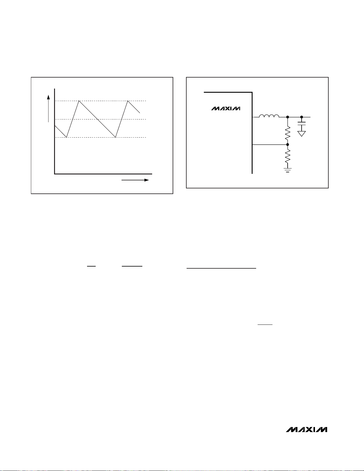
INDUCTOR CURRENT
I
VALLEY
I
LOAD
I
PEAK
Figure 4. Inductor-Current Waveform
MAX8543/
MAX8544
R1
R2
LX
FB
Figure 5. Setting the Output Voltage with a Resistor VoltageDivider
Page 19

MAX8543/MAX8544
Step-Down Controllers with Prebias Startup,
Lossless Sensing, Synchronization, and OVP
______________________________________________________________________________________ 19
A good compromise between size and efficiency is an
LIR of 0.3. Once all the parameters are chosen, the
inductor value is determined as follows:
where fS is the switching frequency. Choose a standardvalue inductor close to the calculated value. The exact
inductor value is not critical and can be adjusted to
make trade-offs among size, cost, and efficiency. Lower
inductor values minimize size and cost, but they also
increase the output ripple and reduce the efficiency due
to higher peak currents. On the other hand, higher inductor values increase efficiency, but eventually resistive
losses due to extra turns of wire exceed the benefit
gained from lower AC current levels. This is especially
true if the inductance is increased without also increasing the physical size of the inductor. Find a low-loss
inductor with the lowest possible DC resistance that fits
the allotted dimensions. Ferrite cores are often the best
choice, although powdered iron is inexpensive and can
work well at 300kHz. The chosen inductor’s saturation
current rating must exceed the peak inductor current
determined as:
Setting the Current Limits
Valley Current Limit
The valley current limit employs a current foldback
scheme. The MAX8543 has a fixed valley current-limit
threshold of 130mV, and a fixed foldback ratio (P
FB
) of
23%. The foldback ratio is the current-limit threshold
when the output is at 0V (output shorted to ground),
divided by the threshold when the output is at its nominal
regulated value. Thus, the minimum output current limit
(I
LIM
) and maximum short-circuit current (ISC) is calculat-
ed as:
where R
DS(ON)
is the maximum on-resistance of the
low-side MOSFET at the highest expected operating
junction temperature, and I
P-P
is the inductor ripple cur-
rent, calculated as:
Ensure that I
LIM
is equal to or greater than the maximum load current at peak current limit (see the Peak
Current Limit section):
where 40mV is the maximum current-limit threshold
when the output is shorted (V
OUT
= 0V).
The MAX8544 has an adjustable valley current limit and
can be selected for foldback with automatic recovery,
or constant current with latch-up. To set the current limit
for foldback mode, connect a resistor from ILIM2 to the
output (R
FOBK
), and another resistor from ILIM2 to
GND (R
ILIM
). See Figure 6. The values of R
FOBK
and
R
ILIM
are calculated as follows:
1) First, select the percentage of foldback (PFB). This
percentage corresponds to the current limit when
V
OUT
equals zero, divided by the current limit when
V
OUT
equals a nominal voltage. A typical value of
P
FB
is in the range of 15% to 40%. A lower value of
PFByields lower short-circuit current. The following
equations are used to calculate R
FOBK
and R
ILIM:
where I
VALLEY
is the value of the inductor valley
current at maximum load (I
LOAD(MAX)
- 1/2 I
P-P
),
and R
DS(ON)
is the maximum on-resistance of the
low-side MOSFET at the highest operating junction
temperature.
R
RI PR
VRI P
ILIM
DS ON VALLEY FB FOBK
OUT DS ON VALLEY FB
=
×××−
()
×
−× × ×−
()
[]
51
51
()
()
R
PV
AP
FOBK
FB OUT
FB
=
×
×−
()
51μ
I
V
R
I
SC
DS ON
PP
=+
−
0042.
()
I
VV V
fLV
PP
IN OUT OUT
SIN
−
=
−
()
×
××
I
V
R
I
LIM
DS ON
PP
=+
−
0112.
()
II
LIR
I
PEAK LOAD MAX LOAD MAX
=+×
() ()
2
L
VVV
V f I LIR
OUT IN OUT
IN S LOAD MAX
=
×−
×× ×
()
()
MAX8544
R
FOBK
R
ILIM
LX
OUT
ILIM2
Figure 6. ILIM2 Resistor Connections
Page 20

MAX8543/MAX8544
Step-Down Controllers with Prebias Startup,
Lossless Sensing, Synchronization, and OVP
20 ______________________________________________________________________________________
2) If the resulting value of R
ILIM
is negative, either
increase P
FB
or choose a low-side MOSFET with a
lower R
DS(ON)
. The latter is preferred as it increases the efficiency and results in a lower short-circuit
current.
To set the constant current limit for the latch-up mode,
only R
ILIM
is used. The equation for R
ILIM
below sets
the current-limit threshold at 1.2 times the maximumrated output current:
Similarly, I
VALLEY
is the value of the inductor valley
current at maximum load, R
DS(ON)
is the maximum onresistance of the low-side MOSFET at the highest operating junction temperature.
Peak Current Limit
Peak inductor current-limit threshold (VTH) has four
possible settings through ILIM (MAX8543) or ILIM1
(MAX8544) as shown in Table 3 below. The resulting
current limit is calculated as:
where RDCis either the DC resistance of the inductor or
the value of the optional current-sense resistor.
Note that V
ILIM
is a logic-level setting, and can allow a
variation of ±0.1 x VVLwithout affecting VTH. To ensure
maximum output current, use the minimum value of V
TH
from each setting, and the maximum RDCvalues at the
highest expected operating temperature. The DC resistance of the inductor’s copper wire has a +0.22%/°C
temperature coefficient.
To use the DC resistance of the output inductor for current sensing, an RC circuit is added (see Figure 7). The
RC time constant is set to be twice the inductor (L / RDC)
time constant. Pick the value of R4 in the range of 470Ω
to 2kΩ, and then calculate the capacitor value from: C9
= 2L / (R
DC
× R4). Add a resistor (R5) equal in value to
R4 to the CS- connection to minimize input-offset error.
The equivalent current-sense resistance is equal to the
DC resistance of the inductor (RDC).
To use a current-sense resistor, connect the resistor as
shown in Figure 8. Since most current-sense resistors
have inductance, the RC circuit is also required
and is calculated in the same manner as inductor
current sensing. Place C11 close to CS+ and CS- pins
to decouple the high-frequency noise pickup. Place
C10 (same value as C9) across R5 to aid in shortcircuit recovery.
I
V
R
I
LIM
THDCPP
=−
−
2
R
IR
A
ILIM
VALLEY DS ON
=
××121.
()
μ
Table 3. ILIM Current-Limit Threshold
Settings
V
ILIM
RECOMMENDED
ILIM CONNECTION
V
TH
MIN
V
TH
TYP
V
TH
MAX
(mV)
0 GND
56.5
1/3 V
VL
Voltage-divider:
200kΩ from ILIM/ILIM1 to VL
115.0
2/3 V
VL
Voltage-divider:
100kΩ from ILIM/ILIM1 to VL
172.5
V
VL
VL
230.0
Figure 8. Using a Current-Sense Resistor
MAX8543/
MAX8544
C9
V
OUT
R4
R5
L1
LX
CS-
CS+
C11
C10
Figure 7. Inductor RDCCurrent Sensing
LX
(mV)
(mV)
38.5 50
100kΩ from ILIM/ILIM1 to GND
200kΩ from ILIM/ILIM1 to GND
85.0 100
127.5 150
170.0 200
MAX8543/
MAX8544
CS+
CS-
L1
C11
R3
R4
C9
V
OUT
C10
R5
Page 21

MAX8543/MAX8544
Step-Down Controllers with Prebias Startup,
Lossless Sensing, Synchronization, and OVP
______________________________________________________________________________________ 21
MOSFET Selection
The MAX8543/MAX8544 drive two or four external,
logic-level, n-channel MOSFETs as the circuit switch
elements. The key selection parameters are:
1) On-resistance (R
DS(ON)
): the lower, the better.
2) Maximum drain-to-source voltage (V
DSS
): should
be at least 20% higher than the input supply rail at
the high-side MOSFET’s drain.
3) Gate charges (QG, QGD, QGS): the lower, the better.
For a 3.3V input application, choose a MOSFET with a
rated R
DS(ON)
at VGS= 2.5V. For a 5V input application,
choose the MOSFETs with rated R
DS(ON)
at VGS≤ 4.5V.
For a good compromise between efficiency and cost,
choose the high-side MOSFET (N1, N2) that has conduction losses equal to the switching loss at nominal input
voltage and output current. The selected low-side
MOSFET (N3, N4) must have an R
DS(ON)
that satisfies the
current-limit-setting condition above. Ensure that the lowside MOSFET does not spuriously turn on due to dV/dt
caused by the high-side MOSFET turning on as this
would result in shoot-through current and degrade the
efficiency. MOSFETs with a lower QGD/ Q
GS
ratio have
higher immunity to dV/dt. For high-current applications, it
is often preferable to parallel two MOSFETs rather than to
use a single large MOSFET.
For proper thermal-management design, the power dissipation must be calculated at the desired maximum
operating junction temperature, maximum output current,
and worst-case input voltage (for the low-side MOSFET,
worst case is at V
IN(MAX)
; for the high-side MOSFET, it
could be either at V
IN(MAX)
or V
IN(MIN)
). The high-side
and low-side MOSFETs have different loss components
due to the circuit operation. The low-side MOSFET operates as a zero-voltage switch; therefore, major losses
are the channel-conduction loss (P
LSCC
) and the body-
diode conduction loss (P
LSDC
):
Use R
DS(ON)
at T
J(MAX)
:
where VFis the body-diode forward-voltage drop, tDTis
the dead time between high-side and low-side switching
transitions, and fSis the switching frequency.
The high-side MOSFET operates as a duty-cycle control
switch and has the following major losses: the channelconduction loss (P
HSCC
), the VI overlapping switching
loss (P
HSSW
), and the drive loss (P
HSDR
). The high-side
MOSFET does not have body-diode conduction loss
because the diode never conducts current:
Use R
DS(ON)
at T
J(MAX)
:
where I
GATE
is the average DH-driver output current
capability determined by:
where R
DS(ON)(HS)
is the high-side MOSFET driver’s
on-resistance (1Ω, typ) and R
GATE
is the internal gate
resistance of the MOSFET (≈0.5Ω to 3Ω):
where V
GS
≈ V
VL.
In addition to the losses above, allow about 20% more for
additional losses due to MOSFET output capacitances
and low-side MOSFET body-diode reverse-recovery
charge dissipated in the high-side MOSFET, but it is not
well defined in the MOSFET data sheet. Refer to the
MOSFET data sheet for thermal resistance specifications
to calculate the PC board area needed to maintain the
desired maximum operating junction temperature with the
above calculated power dissipations.
To reduce EMI caused by switching noise, add a 0.1µF
ceramic capacitor from the high-side switch drain to
the low-side switch source or add resistors in series
with DH and DL to slow down the switching transitions.
However, adding series resistors increases the power
dissipation of the MOSFET, so be sure this does not
overheat the MOSFET.
PQVf
R
RR
HSDR G GS S
GATE
GATE DS ON HS
=× ××
+
()()
I
V
RR
GATE
VL
DS ON HS GATE
≅
×
+
05.
()()
PVI
QQ
I
f
HSSW IN LOAD
GS GD
GATE
S
=× ×
+
×
P
V
V
IR
HSCC
OUT
IN
LOAD
DS ON
=× ×
()
2
PIVtf
LSDC LOAD F DT S
=× × × ×2
P
V
V
IR
LSCC
OUT
IN
LOAD
DS ON
=−
⎛
⎝
⎜
⎞
⎠
⎟
××1
2
()
Page 22

MAX8543/MAX8544
Step-Down Controllers with Prebias Startup,
Lossless Sensing, Synchronization, and OVP
22 ______________________________________________________________________________________
MOSFET Snubber Circuit
Fast switching transitions cause ringing because of resonating circuit parasitic inductance and capacitance at
the switching nodes. This high-frequency ringing
occurs at LX’s rising and falling transitions and can
interfere with circuit performance and generate EMI. To
dampen this ringing, a series RC snubber circuit is
added across each switch. Below is the procedure for
selecting the value of the series RC circuit.
Connect a scope probe to measure VLXto GND and
observe the ringing frequency, fR.
Find the capacitor value (connected from LX to GND)
that reduces the ringing frequency by half.
The circuit parasitic capacitance (C
PAR
) at LX is then
equal to 1/3rd the value of the added capacitance above.
The circuit parasitic inductance (L
PAR
) is calculated by:
The resistor for critical dampening (R
SNUB
) is equal to
2π x fRx L
PAR
. Adjust the resistor value up or down
to tailor the desired damping and the peak voltage
excursion.
The capacitor (C
SNUB
) should be at least 2 to 4 times the
value of the C
PAR
to be effective. The power loss of the
snubber circuit (P
RSNUB
) is dissipated in the resistor and
can be calculated as:
where VINis the input voltage and fSWis the switching
frequency. Choose an R
SNUB
power rating that meets
the specific application’s derating rule for the power
dissipation calculated.
Input Capacitor
The input filter capacitor reduces peak currents drawn
from the power source and reduces noise and voltage
ripple on the input caused by the circuit’s switching.
The input capacitor must meet the ripple-current
requirement (I
RMS
) imposed by the switching currents
defined by the following equation:
I
RMS
has a maximum value when the input voltage equals
twice the output voltage (VIN= 2 x V
OUT
), so I
RMS(MAX)
=
I
LOAD
/ 2. Ceramic capacitors are recommended due to
their low ESR and ESL at high frequency with relatively
low cost. Choose a capacitor that exhibits less than 10°C
temperature rise at the maximum operating RMS current
for optimum long-term reliability. Ceramic capacitors with
an X5R or better temperature characteristic are recommended. When operating from a soft input source, an
additional input capacitor (bulk bypass capacitor) may
be required to prevent input from sagging.
Output Capacitor
The key selection parameters for the output capacitor
are the actual capacitance value, the equivalent series
resistance (ESR), the equivalent series inductance
(ESL), and the voltage-rating requirements. These
parameters affect the overall stability, output voltage
ripple, and transient response. The output ripple has
three components: variations in the charge stored in
the output capacitor, the voltage drop across the
capacitor’s ESR, and ESL caused by the current into
and out of the capacitor. The maximum output voltage
ripple is estimated as follows:
V
RIPPLE
= V
RIPPLE(ESR)
+ V
RIPPLE(C)
+ V
RIPPLE(ESL)
The output voltage ripple as a consequence of the
ESR, ESL, and output capacitance is:
where I
P-P
is the peak-to-peak inductor current:
These equations are suitable for initial capacitor selection, but final values should be chosen based on a prototype or evaluation circuit. As a general rule, a smaller
current ripple results in less output voltage ripple. Since
the inductor ripple current is a factor of the inductor value
and input voltage, the output voltage ripple decreases
with larger inductance, and increases with higher input
voltages. Polymer, tantalum, or aluminum electrolytic
capacitors are recommended.
I
VV
fLVV
PP
IN OUTSOUT
IN
−
=
−
×
×
V
I
Cf
RIPPLE C
PP
OUT S
()
=
××
−
8
V
V
L
ESL
RIPPLE ESLIN()
=×
V I ESR
RIPPLE ESR P P()
=×
−
I
IVVV
V
RMS
LOAD OUT IN OUT
IN
=
×−
()
PCVf
RSNUB SNUB IN SW
=×
()
×
2
L
fC
PAR
R PAR
=
()
×
1
22π
Page 23

MAX8543/MAX8544
Step-Down Controllers with Prebias Startup,
Lossless Sensing, Synchronization, and OVP
______________________________________________________________________________________ 23
The aluminum electrolytic capacitor is the least expensive; however, it has higher ESR. To compensate for this,
use a ceramic capacitor in parallel to reduce the switching ripple and noise. For reliable and safe operation,
ensure that the capacitor’s voltage and ripple-current ratings exceed the calculated values.
The response to a load transient depends on the
selected output capacitors. After a load transient, the
output voltage instantly changes by ESR x ΔI
LOAD
.
Before the controller can respond, the output voltage
deviates further depending on the inductor and output
capacitor values. After a short period of time (see the
Typical Operating Characteristics), the controller
responds by regulating the output voltage back to its
nominal state. The controller response time depends on
its closed-loop bandwidth. With a higher bandwidth,
the response time is faster, thus preventing the output
voltage from further deviation from its regulation value.
Compensation Design
The MAX8543/MAX8544 use an internal transconductance error amplifier whose output compensates the
control loop. The external inductor, output capacitor,
compensation resistor, and compensation capacitors
determine the loop stability. The inductor and output
capacitor are chosen based on performance, size, and
cost. Additionally, the compensation resistor and capacitors are selected to optimize control-loop stability. The
component values, shown in the Typical Application
Circuits (Figures 1 and 2), yield stable operation over the
given range of input-to-output voltages.
The controller uses a current-mode control scheme that
regulates the output voltage by forcing the required current through the external inductor, so the MAX8543/
MAX8544 use the voltage drop across the DC resistance
of the inductor or the alternate series current-sense resistor to measure the inductor current. Current-mode control
eliminates the double pole in the feedback loop caused
by the inductor and output capacitor resulting in a smaller
phase shift and requiring a less elaborate error-amplifier
compensation than voltage-mode control. A simple single
series RCand CCis all that is needed to have a stable,
high-bandwidth loop in applications where ceramic
capacitors are used for output filtering. For other types of
capacitors, due to the higher capacitance and ESR, the
frequency of the zero created by the capacitance and
ESR is lower than the desired closed-loop crossover frequency. To stabilize a nonceramic output-capacitor loop,
add another compensation capacitor (C
F
) from COMP to
GND to cancel this ESR zero.
The basic regulator loop is modeled as a power modulator, output feedback divider, and an error amplifier.
The power modulator has DC gain set by g
mc
x R
LOAD
,
with a pole and zero pair set by R
LOAD
, the output
capacitor (C
OUT
), and its ESR. Below are equations
that define the power modulator:
where R
LOAD
= V
OUT
/ I
OUT(MAX)
, fSis the switching
frequency, L is the output inductance, and gmc=
1 / (A
VCS
× RDC), where A
VCS
is the gain of the current-sense amplifier and RDCis the DC resistance of
the inductor (or current-sense resistor). A
VCS
is
dependent on the current-limit selection at ILIM, and
ranges from 3 to 11 (see Current-Sense Amplifier
Voltage Gain in the Electrical Characteristics table).
The frequencies at which the pole and zero created by
the power modulator are determined as follows:
When C
OUT
is composed of “n” identical capacitors in
parallel, the resulting C
OUT
= n x C
OUT(EACH)
, and ESR
= ESR
(EACH)
/ n. Note that the capacitor zero for a parallel combination of like capacitors is the same as for an
individual capacitor.
The feedback voltage-divider has a gain of GFB= VFB/
V
OUT
, where VFBis equal to 0.8V.
The transconductance error amplifier has a DC gain,
G
EA(DC)
= g
mEA
x RO, where g
mEA
is the error-amplifier
transconductance, which is equal to 110µS, ROis the
output resistance of the error amplifier, which is 10MΩ.
A dominant pole is set by the compensation capacitor
(CC), the amplifier output resistance (RO), and a zero is
set by the compensation resistor (RC) and the compensation capacitor (CC). There is an optional pole set by
CFand RCto cancel the output-capacitor ESR zero if it
occurs near the crossover frequency (fC). Thus:
f
CRR
pdEA
COC
=
×× +
1
2π ()
f
C ESR
zMOD
OUT
=
××
1
2π
f
C
RfL
RfL
ESR
pMOD
OUT
LOAD S
LOAD S
=
××
××
+×
+
⎛
⎝
⎜
⎞
⎠
⎟
1
2π
()
Gg
RfL
RfL
MOD dc mc
LOAD S
LOAD S
()
()
=×
××
+×
Page 24

MAX8543/MAX8544
Step-Down Controllers with Prebias Startup,
Lossless Sensing, Synchronization, and OVP
24 ______________________________________________________________________________________
The crossover frequency, fC, should be much higher
than the power-modulator pole f
PMOD
. Also, fCshould
be less than or equal to 1/5th the switching frequency.
Select a value for fCin the range:
At the crossover frequency, the total loop gain must
equal 1, and is expressed as:
For the case where f
zMOD
is greater than fC:
then R
C
can be calculated as:
where g
mEA
= 110µS.
The error-amplifier compensation zero formed by R
C
and CCshould be set at the modulator pole f
PMOD
. C
C
is calculated by:
If f
zMOD
is less than 5 x fC, add a second capacitor C
F
from COMP to GND. The value of CFis calculated as
follows:
As the load current decreases, the modulator pole also
decreases; however, the modulator gain increases
accordingly and the crossover frequency remains
the same.
For the case where f
zMOD
is less than fC:
The power-modulator gain at fCis:
The error-amplifier gain at fCis:
RCis calculated as:
where g
mEA
= 110µS.
CCis calculated from:
CFis calculated from:
Below is a numerical example to calculate RCand C
C
values of the typical operating circuit of Figure 1
(MAX8544):
A
VCS
= 11 (for ILIM1 = GND)
RDC= 2.5mΩ
gmc= 1 / (A
VCS
x RDC) = 1 / (11 x 0.0025) = 36.7S
V
OUT
= 2.5V
I
OUT(MAX)
= 15A
R
LOAD
= V
OUT
/ I
OUT(MAX)
= 2.5 / 15 = 0.167Ω
C
OUT
= 360µF
ESR = 5mΩ
Gg
RfL
RfL
MOD dc mc
LOAD S
LOAD S
()
()
.
.( ).
.( ).
.
=×
××
+×
=
××××
()
+×××
()
=
−
−
36 36
0 167 600 10 0 8 10
0 167 600 10 0 8 10
450
36
36
C
Rf
F
C zMOD
=
××
1
2π
C
RfLC
RfLR
C
LOAD S OUT
LOAD S C
=
×××
+×
()
×()
R
V
V
f
gG f
C
OUT
FB
C
mEA MOD fc zMOD
=×
××
()
GgR
f
f
EA fc mEA C
zMOD
C
()
=××
GG
f
f
MOD fc MOD dc
pMOD
zMOD
() ( )
=×
C
Rf
F
C zMOD
=
××
1
2π
C
RfLC
RfLR
C
LOAD S OUT
LOAD S C
=
×××
+×
()
×()
R
V
gVG
C
OUT
mEA FB MOD fc
=
××
()
GG
f
f
MOD fc MOD dc
pMOD
C
() ( )
=×
GgR
EA fc mEA C()
=×
GG
V
V
EA fc MOD fc
FB
OUT
() ()
××=1
ff
f
pMOD C
S
<< ≤
5
f
CR
pEA
FC
=
××
1
2πfCR
zEA
CC
=
××
1
2π
Page 25

MAX8543/MAX8544
Step-Down Controllers with Prebias Startup,
Lossless Sensing, Synchronization, and OVP
______________________________________________________________________________________ 25
3.43kHz << fC< 120kHz; select fC= 120kHz.
Since f
zMOD
< fC:
Select the nearest standard value: CC= 220pF
Select the nearest standard value: CF= 10pF:
R3 = RC = 220kΩ
C8 = C
C
= 220pF
C7 = CF= 10pF
Applications Information
PC Board Layout Guidelines
Careful PC board layout is critical to achieve low
switching losses and clean, stable operation. The
switching power stage requires particular attention.
Follow these guidelines for good PC board layout:
1) Place IC decoupling capacitors as close to IC pins
as possible. Keep separate the power ground
plane and the signal ground plane. Place the input
ceramic decoupling capacitor directly across and
as close as possible to the high-side MOSFET’s
drain and the low-side MOSFET’s source. This is to
help contain the high switching current within this
small loop.
2) For output current greater than 10A, a four-layer PC
board is recommended. Pour a signal ground
plane in the second layer underneath the IC to minimize noise coupling.
3) Connect input, output, snubber, and VL capacitors
to the power ground plane; connect all other
capacitors to the signal ground plane.
4) Place the inductor current-sense resistor and capacitor as close to the inductor as possible. Make a
Kelvin connection to minimize the effect of PC board
trace resistance. Place the input bias balance resistor
and bypass capacitor (R5 and C10 in Figures 7 and
8) near CS-. Run two closely parallel traces from
across the capacitor (C9 in Figures 7 and 8) to CS+
and CS-. Place the decoupling capacitor C11 close
to CS+ and CS- pins.
5) Place the MOSFET as close as possible to the IC to
minimize trace inductance of the gate-drive loop. If
parallel MOSFETs are used, keep the trace lengths
to both gates equal.
6) Connect the drain leads of the power MOSFET to a
large copper area to help cool the device. Refer to
the power MOSFET data sheet for recommended
copper area.
7) Place the feedback and compensation components
as close to the IC pins as possible. Connect the
feedback-divider resistor from FB to the output as
close as possible to the farthest output capacitor.
Refer to the MAX8544 evaluation kit for an example layout.
C
Rf
pF
F
C zMOD
=
××
=
××× ×
=
1
2
1
2 220 10 88 4 10
82
33
π
π
()(.)
.
C
RfLC
RfLR
pF
C
LOAD S OUT
LOAD S C
=
×××
+×
()
×
=
×× ×
+× ×
⎛
⎝
⎞
⎠
×
=
−−
−
.( )(. )( )
.( )(. )( )
0 167 600 10 0 8 10 360 10
0 167 600 10 0 8 10 220 10
202
36 6
36 3
R
V
V
f
gG f
k
C
OUT
FB
C
mEA MOD fc zMOD
=×
××
=×
×
××××
=
−
()
.
.
().(.)
25
08
120 10
110 10 0 175 88 4 10
220
3
63
Ω
GG
f
f
MOD fc MOD dc
pMOD
zMOD
() ( )
.
.
.
.
=×
=×
×
×
=45
343 10
88 4 10
0 175
3
3
f
C ESR
kHz
zMOD
OUT
=
××
=
×× ×
=
−
1
2
1
2 360 10 0 005
88 4
6
π
π
().
.
ff
f
pMOD C
S
<< ≤
5
f
C
RfL
RfL
ESR
kHz
pMOD
OUT
LOAD S
LOAD S
=
××
××
+×
+
⎛
⎝
⎜
⎞
⎠
⎟
=
×× ×
××××
⎛
⎝
⎞
⎠
+×××
⎛
⎝
⎞
⎠
+
⎛
⎝
⎜
⎜
⎜
⎞
⎠
⎟
⎟
⎟
=
−
−
−
1
2
1
2 360 10
0 167 600 10 0 8 10
0 167 600 10 0 8 10
0 005
343
6
36
36
π
π
()
.( ).
.( ).
.
.
Page 26
MAX8543/MAX8544
Step-Down Controllers with Prebias Startup,
Lossless Sensing, Synchronization, and OVP
26 ______________________________________________________________________________________
Table 4. Suggested Component Manufacturers
MANUFACTURER COMPONENT WEBSITE PHONE
Central Semiconductor Diodes www.centralsemi.com 631-435-1110
Coilcraft Inductors www.coilcraft.com 800-322-2645
International Rectifier MOSFETs www.irf.com 310-322-3331
Kamaya Resistors www.kamaya.com 260-489-1533
Panasonic Capacitors www.panasonic.com 714-373-7366
Sanyo Capacitors www.sanyo.com 619-661-6835
Sumida Inductors www.sumida.com 847-956-0666
Taiyo Yuden Capacitors www.t-yuden.com 408-573-4150
TDK Capacitors www.component.tdk.com 847-803-6100
Vishay/Siliconix MOSFETs www.vishay.com 402-564-3131
Pin Configurations
Chip Information
TRANSISTOR COUNT: 4185
PROCESS: BiCMOS
TOP VIEW
GND
1
SS
2
COMP
3
MAX8543
4
FB
EN
5
CS-
6
CS+
7
ILIM
8
1
ILIM2
2
GND
3
SS
4
MAX8544
5
FB
6
EN
7
CS-
ILIM1
8
9
10
16
FSYNC
15
BST
14
DH
13
LX
12
IN
VL
11
10
DL
9
PGND
20
SYNCO
19
FSYNC
18
BST
17
DHCOMP
16
LX
15
IN
14
VL
13
DLCS+
12
PGND
11
POKMODE
Page 27

MAX8543/MAX8544
Step-Down Controllers with Prebias Startup,
Lossless Sensing, Synchronization, and OVP
Maxim cannot assume responsibility for use of any circuitry other than circuitry entirely embodied in a Maxim product. No circuit patent licenses are
implied. Maxim reserves the right to change the circuitry and specifications without notice at any time.
Maxim Integrated Products, 120 San Gabriel Drive, Sunnyvale, CA 94086 408-737-7600 ____________________ 27
© 2004 Maxim Integrated Products Printed USA is a registered trademark of Maxim Integrated Products.
Package Information
(The package drawing(s) in this data sheet may not reflect the most current specifications. For the latest package outline information,
go to www.maxim-ic.com/packages.)
QSOP.EPS
 Loading...