

Page 1
General Description
The MAX8537/MAX8539 controllers provide a complete
power-management solution for both double-data-rate
(DDR) and combiner supplies. The MAX8537 and
MAX8539 are configured for out-of-phase and in-phase
DDR power-supply operations, respectively, and generate three outputs: the main memory voltage (V
DDQ
), the
tracking sinking/sourcing termination voltage (V
TT
), and
the termination reference voltage (V
TTR
). The MAX8538
is configured as a dual out-of-phase controller for pointof-load supplies. Each buck controller can source or
sink up to 25A of current, while the termination reference can supply up to 15mA output.
The MAX8537/MAX8538/MAX8539 use constantfrequency voltage-mode architecture with operating
frequencies of 200kHz to 1.4MHz. An internal highbandwidth (25MHz) operational amplifier is used as an
error amplifier to regulate the output voltage. This
allows fast transient response, reducing the number of
output capacitors. An all-N-FET design optimizes efficiency and cost. The MAX8537/MAX8538/MAX8539
have a 1% accurate reference. The second synchronous buck controller in the MAX8537/MAX8539 and the
VTTR amplifier generate 1/2 V
DDQ
voltage for VTTand
V
TTR
, and track the V
DDQ
within ±1%.
This family of controllers uses a high-side current-sense
architecture for current limiting. ILIM pins allow the setting of an adjustable, lossless current limit for different
combinations of load current and R
DSON
. Alternately,
more accurate overcurrent limit is achieved by using
a sense resistor in series with the high-side FET.
Overvoltage protection is achieved by latching off the
high-side MOSFET and latching on the low-side MOSFET
when the output voltage exceeds 17% of its set output.
Independent enable, power-good, and soft-start features
enhance flexibility.
Applications
DDR Memory Power Supplies
Notebooks and Desknotes
Servers and Storage Systems
Broadband Routers
XDSL Modems and Routers
Power DSP Core Supplies
Power Combiner in Advanced VGA Cards
Networking Systems
RAMBUS Memory Power Supplies
Features
♦ MAX8537/MAX8539: Complete DDR Supplies
♦ MAX8538: Dual Nontracking Controller
♦ Out-of-Phase (MAX8537/MAX8538) or In-Phase
(MAX8539) Operation
♦ 4.5V to 23V Wide Input Range (Operate Down to
1.8V Input with External 5V Supply)
♦ Tracking Supply Maintains VTT= V
TTR
= 1/2 V
DDQ
♦ Adjustable Output from 0.8V to 3.6V with 1%
Accuracy
♦ VTTR Reference Sources and Sinks Up to 15mA
♦ 200kHz to 1.4MHz Adjustable Switching
Frequency
♦ All-Ceramic Design Achievable
♦ >90% Efficiency
♦ Independent POK_ and EN_
♦ Adjustable Soft-Start and Soft-Stop for Each
Output
♦ Lossless Adjustable-Hiccup Current Limit
♦ Output Overvoltage Protection
♦ 28-Pin QSOP Package
MAX8537/MAX8538/MAX8539
Dual-Synchronous Buck Controllers for Point-of-
Load, Tracking, and DDR Memory Power Supplies
________________________________________________________________ Maxim Integrated Products 1
19-3141; Rev 1; 6/05
For pricing, delivery, and ordering information, please contact Maxim/Dallas Direct! at
1-888-629-4642, or visit Maxim’s website at www.maxim-ic.com.
EVALUATION KIT
AVAILABLE
Ordering Information
Pin Configurations appear at end of data sheet.
+Denotes lead-free package.
PART TEMP RANGE
MAX8537EEI -40°C to +85°C 28 QSOP
M AX 8537E E I+ -40°C to +85°C 28 QSOP
MAX8538EEI -40°C to +85°C 28 QSOP
M AX 8538E E I+ -40°C to +85°C 28 QSOP
MAX8539EEI -40°C to +85°C 28 QSOP
M AX 8539E E I+ -40°C to +85°C 28 QSOP
PIN-
PACKAGE
OPERATION
Out-of-phase
tracking
Out-of-phase
tracking
Out-of-phase
nontracking
Out-of-phase
nontracking
In-phase
tracking
In-phase
tracking
Page 2
MAX8537/MAX8538/MAX8539
Dual-Synchronous Buck Controllers for Point-ofLoad, Tracking, and DDR Memory Power Supplies
2 _______________________________________________________________________________________
ABSOLUTE MAXIMUM RATINGS
Stresses beyond those listed under “Absolute Maximum Ratings” may cause permanent damage to the device. These are stress ratings only, and functional
operation of the device at these or any other conditions beyond those indicated in the operational sections of the specifications is not implied. Exposure to
absolute maximum rating conditions for extended periods may affect device reliability.
V+ to GND ..............................................................-0.3V to +25V
AVL, VL to GND........................................................-0.3V to +6V
PGND to GND .......................................................-0.3V to +0.3V
FB_, EN_, POK_ to GND...........................................-0.3V to +6V
REFIN, VTTR, FREQ, SS_, COMP_ to GND....-0.3V to (AVL + 0.3V)
BST_, ILIM_ to GND ...............................................-0.3V to +30V
DH1 to LX1 ...............................................-0.3V to (BST1 + 0.3V)
DH2 to LX2 ...............................................-0.3V to (BST2 + 0.3V)
LX_ to BST_ ..............................................................-6V to +0.3V
LX_ to GND................................................................-2V to +25V
DL_ to PGND ................................................-0.3V to (VL + 0.3V)
Continuous Power Dissipation (T
A
= +70°C)
28-Pin QSOP (derate 10.8mW/°C above +70°C)........860mW
Operating Temperature Range ...........................-40°C to +85°C
Junction Temperature......................................................+150°C
Storage Temperature Range .............................-65°C to +150°C
Lead Temperature (soldering, 10s) ..........................……+300°C
ELECTRICAL CHARACTERISTICS
(V+ = 12V, EN_ = VL, BST_ = 6V, LX_ = 1V, VL load = 0mA, CVL= 10µF (ceramic), REFIN = 1.25V, PGND = AGND = FB_ = ILIM_ =
0V, C
SS
= 10nF, C
VTTR
= 1µF, R
FREQ
= 20kΩ, DH_ = open, DL_ = open, POK_ = open, circuit of Figure 1, TA= 0°C to +85°C, unless
otherwise noted.)
PARAMETER CONDITIONS MIN TYP MAX UNITS
GENERAL
V+ Operating Range VL regulator drops out below 5.5V (Note 1) 4.5 23.0 V
V+/ VL Operating Range VL is externally generated (Note 1) 4.5 5.5 V
V+ Operating Supply Current IL(VL) = 0, FB_ forced 50mV above threshold 3.5 7 mA
V+ Standby Supply Current IL(VL) = 0, BST_ = VL, EN = LX_ = FB_ = 0V 350 700 µA
VL REGULATOR
Output Voltage 5.5V < V+ < 23V, 1mA < I
VL Undervoltage-Lockout Trip
Level
Output Current
Rising edge, hysteresis = 550mV (typ) (trip level is
typically 85% of VL)
This is for gate current of DL_ /DH_ drivers, C(VL) =
1µF/10mA ceramic capacitor
Thermal Shutdown Rising temperature, typical hysteresis = 10°C +160 °C
CURRENT-LIMIT THRESHOLD (all current limits are tested at V+ = VL = 4.5V and 5.5V)
ILIM Sink Current ILIM_ = LX - 200mV, 1.8V < LX < 23V, BST = LX +5V 180 200 220 µA
SOFT-START
Soft-Start Source Current SS_ = 100mV -7 -5 -3 µA
Soft-Start Sink Current SS_ = 0.8 or REFIN 3 5 7 µA
Soft-Start Full-Scale Voltage
FREQUENCY
Low End of Range R
Intermediate Range R
High End of Range R
= 100kΩ, V+ = VL = 5V 160 200 240 kHz
FREQ
= 20kΩ, V+ = VL = 5V 800 1000 1200 kHz
FREQ
= 14.3kΩ, V+ = VL = 5V 1120 1400 1680 kHz
FREQ
R
= 100kΩ 95
FREQ
R
= 20kΩ 80 Maximum Duty Cycle
FREQ
R
= 14.3kΩ 72
FREQ
< 70mA 4.75 5 5.25 V
LOAD
4.18 4.3 4.42 V
70 mA
0.8 or
REFIN
V
%
Page 3
MAX8537/MAX8538/MAX8539
Dual-Synchronous Buck Controllers for Point-of-
Load, Tracking, and DDR Memory Power Supplies
_______________________________________________________________________________________ 3
ELECTRICAL CHARACTERISTICS (continued)
(V+ = 12V, EN_ = VL, BST_ = 6V, LX_ = 1V, VL load = 0mA, CVL= 10µF (ceramic), REFIN = 1.25V, PGND = AGND = FB_ = ILIM_ =
0V, C
SS
= 10nF, C
VTTR
= 1µF, R
FREQ
= 20kΩ, DH_ = open, DL_ = open, POK_ = open, circuit of Figure 1, TA= 0°C to +85°C, unless
otherwise noted.)
PARAMETER CONDITIONS MIN TYP MAX UNITS
R
= 100kΩ 2.4 4
FREQ
R
= 20kΩ 12 18Minimum Duty Cycle
FREQ
R
= 14.3kΩ 16 25
FREQ
DH_ Minimum Off-Time 140 200 ns
DH_ Minimum On-Time 120 ns
%
ERROR AMPLIFIER
FB_ Input Bias Current V
_ = 0.8V 250 nA
FB
FB1 Input-Voltage Set Point Over line and load 0.792 0.800 0.808 V
FB2 Input-Voltage Set Point
Op-Amp Open-Loop Voltage
Gain
Op-Amp Gain Bandwidth 25 MHz
Op-Amp Output-Voltage Slew
Rate
MAX8538 0.792 0.800 0.808
MAX8537/MAX8539, REFIN = 0.9V 0.894 0.900 0.906
COMP_ = 1.3V to 2.3V 72 >80 dB
15 V/µs
V
DRIVERS
Break-Before-Make Time 30 ns
DH1, DH2 On-Resistance in Low
State
DH1, DH2 On-Resistance in High
State
DL1, DL2 On-Resistance in Low
State
DL1, DL2 On-Resistance in High
State
0.9 2.5 Ω
1.3 2.5 Ω
0.7 1.5 Ω
1.6 2.8 Ω
LOGIC INPUTS (EN_)
Input Low Level 4.5V < VL < 5.5V 0.8 V
Input High Level 4.5V < VL < 5.5V 2.4 V
Input Bias Current 0V to 5.5V -1 +0.1 +1 µA
VTTR
VTTR Output Voltage Range Source or sink 15mA 0.5 2.5 V
VTTR Output Accuracy -15mA ≤ I
≤ +15mA, REFIN = 0.9V or 1.25V -1.0 REFIN +1.0 %
VTTR
REFIN
REFIN Input Bias Current REFIN = 0.9V or 1.25V -250 +250 nA
Page 4
MAX8537/MAX8538/MAX8539
Dual-Synchronous Buck Controllers for Point-ofLoad, Tracking, and DDR Memory Power Supplies
4 _______________________________________________________________________________________
ELECTRICAL CHARACTERISTICS (continued)
(V+ = 12V, EN_ = VL, BST_ = 6V, LX_ = 1V, VL load = 0mA, CVL= 10µF (ceramic), REFIN = 1.25V, PGND = AGND = FB_ = ILIM_ =
0V, C
SS
= 10nF, C
VTTR
= 1µF, R
FREQ
= 20kΩ, DH_ = open, DL_ = open, POK_ = open, circuit of Figure 1, TA= 0°C to +85°C, unless
otherwise noted.)
ELECTRICAL CHARACTERISTICS (Note 2)
(V+ = 12V, EN_ = VL, BST_ = 6V, LX_ = 1V, VL load = 0mA, CVL= 10µF (ceramic), REFIN = 1.25V, PGND = AGND = FB_ = ILIM_ =
0V, C
SS
= 10nF, C
VTTR
= 1µF, R
FREQ
= 20kΩ, DH_ = open, DL_ = open, POK_ = open, circuit of Figure 1, TA= -40°C to +85°C,
unless otherwise noted.)
Note 1: Operating supply range is guaranteed by the VL line-regulation test. User must short V+ to VL if a fixed 5V supply is used
(i.e., if V+ is less than 5.5V).
Note 2: Specifications to -40°C are guaranteed by design, not production tested.
PARAMETER CONDITIONS MIN TYP MAX UNITS
REFIN Input Voltage Range 0.5 2.5 V
REFIN Undervoltage-Lockout Trip
Level
OUTPUT-VOLTAGE FAULT COMPARATORS
Upper FB2 Fault Threshold Rising voltage, hysteresis = 15mV 115 117 120
Lower FB2 Fault Threshold Falling voltage, hysteresis = 15mV 68 70 72
Upper FB1 Fault Threshold Rising voltage, hysteresis = 15mV 115 117 120
Lower FB1 Fault Threshold Falling voltage, hysteresis = 15mV 68 70 72
POWER-OK OUTPUT (POK_)
POK_ Delay 64
Upper FB2 POK_ Threshold Rising voltage, hysteresis = 20mV 110 112 114
Lower FB2 POK_ Threshold Falling voltage, hysteresis = 20mV 86 88 90
Rising and falling edge, hysteresis = 15mV 0.4 0.45 0.5 V
Upper FB1 POK_ Threshold Rising voltage, hysteresis = 20mV 110 112 114
Lower FB1 POK_ Threshold Falling voltage, hysteresis = 20mV 86 88 90
POK_ Output Low Level I
POK_ Output High Leakage POK_ = 5.5V 1 µA
= 2mA 0.4 V
SINK
% of
REFIN
% of
REFIN
% of
0.8V
% of
0.8V
Clock
cycles
% of
REFIN
% of
REFIN
% of
0.8V
% of
0.8V
PARAMETER CONDITIONS MIN TYP MAX UNITS
V+ Operating Range VL regulator drops out below 5.5V (Note 1) 4.75 23.00 V
FB_ Input-Voltage Set Point Over line and load 0.788 0.800 0.812 V
FB2 Input-Voltage Set Point MAX8537/MAX8539, REFIN = 0.9V 0.891 0.900 0.909 V
VTTR Output Accuracy -15mA < I
≤ +15mA, REFIN = 0.9V or 1.25V -1 REFIN +1 %
VTTR
Page 5
MAX8537/MAX8538/MAX8539
Dual-Synchronous Buck Controllers for Point-of-
Load, Tracking, and DDR Memory Power Supplies
_______________________________________________________________________________________ 5
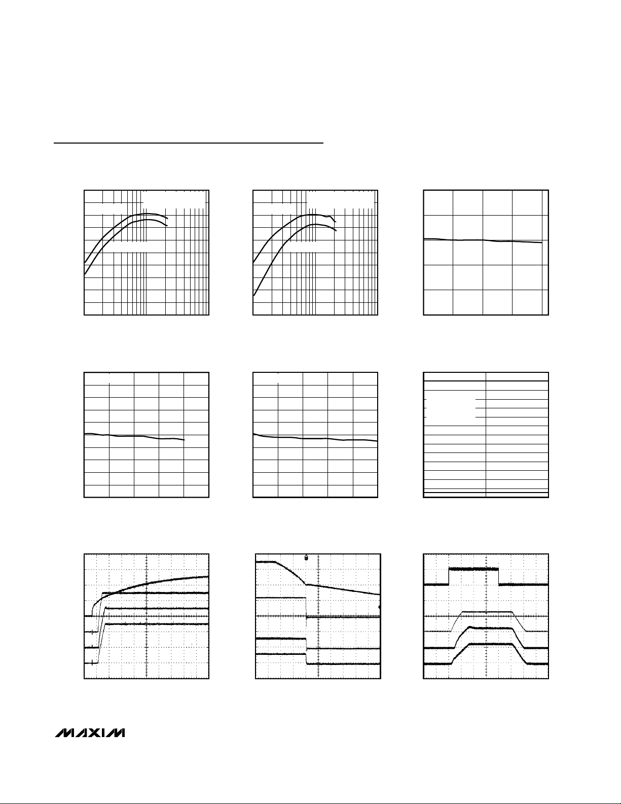
Typical Operating Characteristics
(Circuit of Figure 1, TA= +25°C, 400kHz switching frequency, VIN= 12V, unless otherwise noted.)
V
100
95
V
= 2.5V
DDQ
90
85
80
75
70
EFFICIENCY (%)
65
60
55
50
1100
SENSE RESISTOR = 0
V
= 1.8V
DDQ
10
LOAD CURRENT (A)
V
IN
= 12V
Ω
MAX8537 toc01
EFFICIENCY vs. LOAD CURRENT
DDQ
VTT vs. LOAD CURRENT
1.30
VIN = 12V
1.29
1.28
1.27
1.26
TT
V
1.25
1.24
1.23
1.22
1.21
1.20
015
LOAD CURRENT (A)
12963
MAX8537 toc04
V
EFFICIENCY vs. LOAD CURRENT
DDQ
100
95
V
= 2.5V
DDQ
90
85
80
75
70
EFFICIENCY (%)
65
60
55
50
1100
V
1.30
VIN = 12V
1.29
1.28
1.27
1.26
TTR
1.25
V
1.24
1.23
1.22
1.21
1.20
025
SENSE RESISTOR = 3m
V
= 1.8V
DDQ
10
LOAD CURRENT (A)
vs. LOAD CURRENT
TTR
LOAD CURRENT (mA)
Ω
= 12V
V
IN
2015105
2.55
MAX8537 toc02
2.53
2.51
DDQ
V
2.49
2.47
2.45
2.6
2.5
2.4
MAX8537 toc05
2.3
2.2
2.1
2.0
1.9
1.8
1.7
OUTPUT VOLTAGE (V)
1.6
1.5
1.4
1.3
1.2
V
vs. LOAD CURRENT
DDQ
VIN = 12V
0
LOAD CURRENT (A)
2015105
OUTPUT VOLTAGE vs. INPUT VOLTAGE
V
DDQ
I
= 20A
OUT_VDDQ
= 12A
I
OUT_VTT
= 15mA
I
OUT_VTTR
VTT AND V
TTR
12 14
13
INPUT VOLTAGE (V)
MAX8537 toc03
MAX8537 toc06
POWER-UP
4ms/div
MAX8537 toc07
V+
5V/div
V
DDQ
1V/div
V
TT
8.5V/div
V
TTR
8.5V/div
V
IN
V
DDQ
V
TT
V
VTTR
POWER-DOWN
4ms/div
MAX8537 toc08
5V/div
2V/div
2V/div
2V/div
STARTUP AND SHUTDOWN
1ms/div
MAX8537 toc09
EN1/EN2
5V/div
V
DDQ
2V/div
V
TT
1V/div
V
TTR
1V/div
Page 6
MAX8537/MAX8538/MAX8539
Dual-Synchronous Buck Controllers for Point-ofLoad, Tracking, and DDR Memory Power Supplies
6 _______________________________________________________________________________________
Typical Operating Characteristics (continued)
(Circuit of Figure 1, TA= +25°C, 400kHz switching frequency, VIN= 12V, unless otherwise noted.)
I
OUT_VDDQ
I
OUT_VTT
= 20A
= 8A
POWER-OK
2ms/div
MAX8537 toc10
V
DDQ
2V/div
POK1
5V/div
V
TT
1V/div
POK2
5V/div
VTT LOAD-TRANSIENT RESPONSE
-8A
8A
di/dt = 1A/µs
I
OUT_VDDQ
I
OUT_VTTR
200µs/div
VTT STARTUP AND SHUTDOWN
2ms/div
MAX8537 toc13
V
TT
AC-COUPLED
50mV/div
V
TTR
AC-COUPLED
50mV/div
V
DDQ
AC-COUPLED
50mV/div
V
TT_IOUT
10A/div
= 20A
= 15mA
MAX8537 toc11
EN2
5V/div
V
TT
1V/div
V
TTR
1V/div
V
DDQ
2V/div
V
= 2.5V AT 20A BODE PLOT,
DDQ
180
160
140
120
100
80
60
dB (DEGREES)
40
20
0
-20
-40
100 1M
20A
10A
V
IN
VTT_I
V
TTR
= 12V
kHz
V
LOAD TRANSIENT
DDQ
AND V
di/dt
= 12A
OUT
= 15mA
200µs/div
100k10k1k
TRACKING
TT
= 5A/µs
MAX8537 toc12
MAX8537 toc14
V
DDQ
100mV/div
V
TT
50mV/div
V
TTR
50mV/div
V
DDQ_IOUT
10A/div
VTT = 1.25V AT 12A BODE PLOT,
150
125
100
75
50
dB (DEGREES)
25
0
-25
-50
2
10
IN
MAX8537 toc15
3
10
4
10
Hz
5
10
6
10
SHORT CIRCUIT AND RECOVERY
V
OUT1
V
OUT2
I
L1
I
IN
MAX8537 toc16
10ms/div
= 12V
V
1V/div
1V/div
10V/div
5A/div
Page 7
MAX8537/MAX8538/MAX8539
Dual-Synchronous Buck Controllers for Point-of-
Load, Tracking, and DDR Memory Power Supplies
_______________________________________________________________________________________ 7
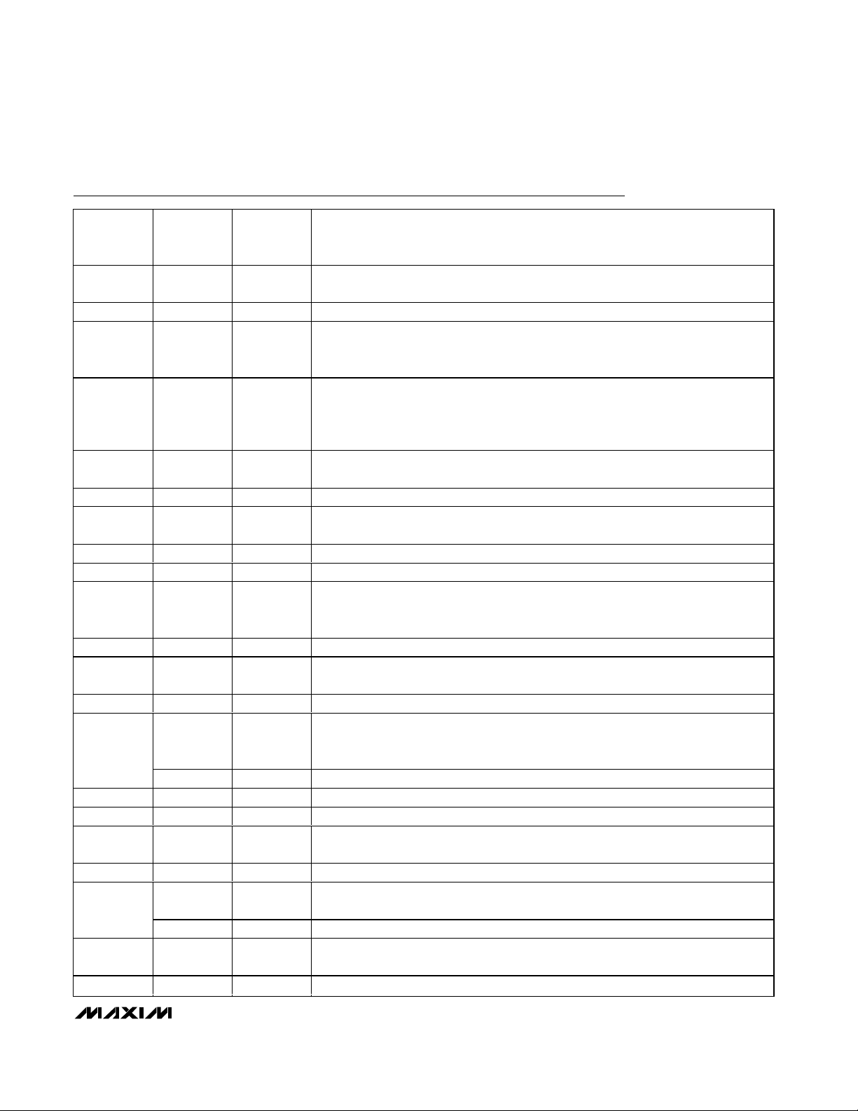
Pin Description
NAME
PIN
1 BST2 BST2
2 DH2 DH2 High-Side Gate-Driver Output for Step-Down 2. Swings from LX2 to BST2.
3 LX2 LX2
4 ILIM2 ILIM2
5 POK1 POK1
6 DL2 DL2 Low-Side Gate-Driver Output for Step-Down 2. Swings from PGND to VL.
7 POK2 POK2
8 EN2 EN2 Enable Input for Step-Down 2 (also for VTTR for the MAX8537 and MAX8539)
9 EN1 EN1 Enable Input for Step-Down 1
10 FREQ FREQ
11 COMP2 COMP2 Compensation Pin for Step-Down 2. Connect to compensation networks.
12 FB2 FB2
13 SS2 SS2 Soft-Start for Step-Down 2. Connect a capacitor to GND to set the soft-start time.
14
15 GND GND Analog Ground for Internal Circuitry
16 SS1 SS1 Soft-Start for Step-Down 1. Connect a capacitor to GND to set the soft-start time.
17 FB1 FB1
18 COMP1 COMP1 Compensation Pin for Step-Down 1. Connect to compensation networks.
19
20 AVL AVL
21 V+ V+ Input Supply Voltage
(MAX8537/
MAX8539)
REFIN —
— N.C. For the MAX8538, connect pin 14 to GND.
VTTR —
— GND Analog Ground for Internal Circuitry
NAME
(MAX8538)
FUNCTION
Bootstrap Input to Power Internal High-Side Driver for Step-Down 2. Connect to an
external capacitor and diode according to Figure 1.
External Inductor Input for Step-Down 2. Connect to the switched side of the inductor.
LX2 serves as the lower supply-voltage rail for the DH2 high-side gate driver and the
current-limit circuitry.
Output Current-Limit Setting for Step-Down 2. Connect a resistor from ILIM2 to the
drain of the step-down 2 high-side MOSFET, or to the junction of the source of the
high-side MOSFET and the current-sense resistor to set the current-limit threshold.
See the Current-Limit Setting section.
Open-Drain Output. High impedance when step-down 1 is within 12% of its regulation
voltage. POK1 is pulled low in shutdown.
Open-Drain Output. High impedance when step-down 2 is within 12% of its regulation
voltage. POK2 is pulled low in shutdown or if REFIN is undervoltage.
Frequency Adjust. Connect a resistor from this pin to ground to set the frequency. The
range of the FREQ resistor is 163kΩ, 20kΩ, and 100kΩ (corresponding to 1.4MHz,
1.0MHz, and 200kHz).
Feedback Input for Step-Down 2 with V
impedance <40kΩ.
Reference Input for V
common-mode voltage range is 0.5V to 2.5V. Current through the divider-resistors
must be ≥100µA.
Feedback Input for Step-Down 1 with 0.8V Threshold. User must have impedance
<40kΩ.
VTTR Output Capable of Sourcing and Sinking Up to 15mA. Always bypass with a 1µF
ceramic capacitor (or larger) to GND.
Analog VL Input Pin. Connect to VL through a 4.7Ω resistor. Bypass with a 0.1µF (or
larger) ceramic capacitor to GND.
TT
and V
. Connect it to a resistor-divider from V
TTR
as the Threshold. User must have
REFIN
DDQ
. REFIN
Page 8

MAX8537/MAX8538/MAX8539
Detailed Description
The MAX8537/MAX8539 controllers provide a complete
power-management solution for both DDR and combiner supplies. The MAX8537 and MAX8539 are configured for out-of-phase and in-phase DDR power-supply
operations, respectively. In addition to the dual-synchronous buck controllers, they also contain an additional amplifier to generate a total of three outputs: the
main memory voltage (V
DDQ
), the tracking
sinking/sourcing termination voltage (VTT), and the termination reference voltage (V
TTR
). The MAX8538 is
configured as a dual out-of-phase controller for pointof-load supplies. Each buck controller can source or
sink up to 25A of current, while the termination reference can supply up to 15mA output.
The MAX8537/MAX8539 have a 1% accurate reference. The first buck controller generates V
DDQ
using
external resistor-dividers. The second synchronous
buck controller and the amplifier generate 1/2 V
DDQ
voltage for VTTand V
TTR
. The VTTand V
TTR
voltages
are maintained within 1% of 1/2 V
DDQ
.
The MAX8537/MAX8538/MAX8539 use a constant-frequency voltage-mode architecture with operating frequencies of 200kHz to 1.4MHz to allow flexible design.
An internal high-bandwidth (25MHz) operational amplifier is used as an error amplifier to regulate the output
voltage. This allows fast transient response, reducing
the number of output capacitors. Synchronous rectification ensures high efficiency and balanced current
sourcing and sinking capability for VTT. An all-N-FET
design optimizes efficiency and cost. The two converters can be operated in-phase or out-of-phase to minimize capacitance and optimize performance for all
VIN/V
OUT
combinations.
Both channels have independent enable and powergood functions. They also have high-side current-sense
architectures. ILIM pins allow the setting of an
adjustable, lossless current limit for different combinations of load current and R
DS(ON)
. Additionally, accurate overcurrent protection is achieved by using a
sensing resistor in series with the high-side FET. The
positive current-limit threshold is programmable
through an external resistor. Overvoltage protection is
achieved by latching off the high-side MOSFET and
latching on the low-side MOSFET when the output voltage exceeds 17% of its set output.
Dual-Synchronous Buck Controllers for Point-ofLoad, Tracking, and DDR Memory Power Supplies
8 _______________________________________________________________________________________
Pin Description (continued)
NAME
PIN
22 VL VL
23 DL1 DL1 Low-Side Gate-Driver Output for Step-Down 1. Swings from PGND to VL.
24 PGND PGND Power Ground for Gate-Driver Circuits
25 ILIM1 ILIM1
26 LX1 LX1
27 DH1 DH1 High-Side Gate-Driver Step-Down 1. Swings from LX1 to BST1.
28 BST1 BST1
(MAX8537/
MAX8539)
NAME
(MAX8538)
FUNCTION
Internal 5V Linear Regulator to Power the IC. VL is always on. Bypass with a ceramic
capacitor with 1µF/10mA of load current. The internal VL regulator can be disabled by
connecting VL and V+ to an externally generated 5V. VL output current can be
boosted with an external PNP transistor.
Output Current-Limit Setting for Step-Down 1. Connect a resistor from ILIM1 to the
drain of the step-down 1 high-side MOSFET, or to the junction of the source of the
high-side MOSFET and the current-sense resistor to set the current-limit threshold.
See the Current-Limit Setting section.
External Inductor Input for Step-Down 1. Connect to the switched side of the inductor.
LX1 serves as the lower supply-voltage rail for the DH1 high-side gate driver and
current-limit circuitry.
Bootstrap Input to Power Internal High-Side Driver for Step-Down 1. Connect to an
external capacitor and diode according to Figure 1.
Page 9

DC-DC Controller
The MAX8537/MAX8538/MAX8539 step-down DC-DC
converters use a PWM voltage-mode control scheme.
An internal high-bandwidth (25MHz) operational amplifier is used as an error amplifier to regulate the output
voltage. The output voltage is sensed and compared
with an internal 0.8V reference or REFIN to generate an
error signal. The error signal is then compared with a
fixed-frequency ramp by a PWM comparator to give the
appropriate duty cycle to maintain output voltage regulation. At the rising edge of the internal clock, and with DL
(the low-side MOSFET gate drive) at 0V, the high-side
MOSFET turns on. When the ramp voltage reaches the
error-amplifier output voltage, the high-side MOSFET
latches off until the next clock pulse. During the highside MOSFET on-time, current flows from the input,
through the inductor, and to the output capacitor and
load. At the moment the high-side MOSFET turns off,
the energy stored in the inductor during the on-time is
released to support the load as the inductor current
ramps down by commutation through the low-side
MOSFET body diode. After a fixed delay, the low-side
MOSFET turns on to shunt the current from its body
diode for lower voltage drop and increased efficiency.
The low-side MOSFET turns off at the rising edge of the
next clock pulse, and when its gate voltage discharges
to zero, the high-side MOSFET turns on and another
cycle starts.
The controllers sense peak inductor current and provide hiccup-mode overload and short-circuit protection
(see the Current Limit section).
The MAX8537/MAX8538/MAX8539 operate in forcedPWM mode where the inductor current is always continuous, so even under light load the controller maintains
a constant switching frequency to minimize noise and
possible interference with system circuitry.
Synchronous-Rectifier Driver (DL)
Synchronous rectification reduces the conduction loss
in the rectifier by replacing the normal Schottky catch
diode with a low-resistance MOSFET switch. The
MAX8537/MAX8538/MAX8539 controllers also use the
synchronous rectifier to ensure proper startup of the
boost gate-drive circuit.
High-Side Gate-Drive Supply (BST)
Gate-drive voltage for the high-side N-channel switch is
generated by a flying-capacitor boost circuit (Figure 1).
The capacitor between BST and LX is alternately
charged from the VL supply and placed in parallel to
the high-side MOSFET’s gate-source terminals.
On startup, the synchronous rectifier (low-side
MOSFET) forces LX to ground and charges the boost
capacitor to VL. On the second half-cycle, the switchmode power supply turns on the high-side MOSFET by
closing an internal switch between BST and DH. This
provides the necessary gate-to-source voltage to turn
on the high-side switch, an action that boosts the 5V
gate-drive signal above the input voltage.
Internal 5V Linear Regulator
All MAX8537/MAX8538/MAX8539 functions are powered from the on-chip low-dropout 5V regulator with the
input connected to V+. Bypass the regulator’s output
(VL) with a 1µF/10mA or greater ceramic capacitor. The
V+ to VL dropout voltage is typically 500mV, so when
V+ is less than 5.5V, VL is typically (V+ - 500mV).
The internal linear regulator can source up to 70mA to
supply the IC, power the low-side gate drivers, and
charge the external boost capacitors. The current
required to drive the external MOSFETs is calculated as
the total gate charge of the MOSFETs at 5V multiplied
by the switching frequency. At higher frequency, the
MOSFET drive current may exceed the capability of the
internal linear regulator. The output current at VL can
be supplemented with an external PNP transistor as
shown in Figures 4 and 5, which also moves most of
the power dissipation off the IC. The external PNP can
increase the output current at VL to over 200mA. The
dropout voltage increases to 1V (typ).
Undervoltage Lockout (UVLO)
If VL drops below 3.75V, the MAX8537/MAX8538/
MAX8539 assume that the supply voltage is too low to
make valid decisions, so UVLO circuitry inhibits switching and forces POK and DH low and DL high. After VL
rises above 4.3V, the controller powers up the outputs
(see the Startup section).
Startup
Externally, the MAX8537/MAX8538/MAX8539 start
switching when VL rises above the 4.3V UVLO threshold. However, the controller does not start unless all
four of the following conditions are met: 1) EN_ is high,
2) VL > 4.3V, 3) the internal reference exceeds 80% of
its nominal value (V
REF
> 0.64V), and 4) the thermal
limit is not exceeded. Once the MAX8537/MAX8538/
MAX8539 assert the internal enable signal, the controller starts switching and enables soft-start.
MAX8537/MAX8538/MAX8539
Dual-Synchronous Buck Controllers for Point-of-
Load, Tracking, and DDR Memory Power Supplies
_______________________________________________________________________________________ 9
Page 10

MAX8537/MAX8538/MAX8539
Dual-Synchronous Buck Controllers for Point-ofLoad, Tracking, and DDR Memory Power Supplies
10 ______________________________________________________________________________________
Figure 1. Typical Application Circuit: MAX8537 DDR Memory Application (400kHz Switching)
VOUT1
2.5V/20A
VIN (10.8V TO 13.2V)
µF
L1
N3N4
C3
C28
1000µF
C29
1000µF
1000µF
C4
10µF
C6
0.47µF
27
28
DH1
BST1
VL
D1 D2
U1
MAX8537
BST2
DH2
1
2
R4
0.003Ω
R25
3.3Ω
C9
47pF
25
26
LX1
ILIM1
ILIM2
LX2
3
456
220
C12, C36
0.9µH
N7
N8
C42
0.15µF
R3
402Ω
23
24
DL1
PGND
DL2
POK1
R7
2.2Ω
C13
10µF
VL
21
22
VL
POK2
EN2
7
8
VTTR
C22
820pF
C16
1µF
C14
1µF
R8
4.7Ω
C15
1µF
20
V+
AVL
EN1
9
R13
1.2kΩ
R14
22kΩ
C21
3.9nF
C20
18
19
VTTR
COMP1
FREQ
10
39pF
COMP2
11
R15
21.5kΩ
R16
10.0kΩ
C24
0.01µF
15
16
17
FB1
SS1
GND
FB2
SS2
12
REFIN
13
14
R18
10.0kΩ
C8
3.3Ω
C31, C32
C11, C30,
VOUT2
1.25V/
C41
R1
680µF
±12A
47pF
47nF
0.005Ω
R2
402Ω
N5
VL
R6
100kΩ
R5
100kΩ
L2
0.8uH
R20
R19
100kΩ
100kΩ
POK1
POK2
C5
0.47µF
R24
C1
1000µF
C26
C27
1000µF
1000µF
N1
C2
10µF
EN2
EN1
R9
51.1kΩ
C17
3.9nF
R11
51kΩ
R10
10.0kΩ
C18
R12
15pF
510Ω
C23
0.01µF
C19
8.2nF
R17
C25
10.0kΩ
220pF
Page 11

MAX8537/MAX8538/MAX8539
Dual-Synchronous Buck Controllers for Point-of-
Load, Tracking, and DDR Memory Power Supplies
______________________________________________________________________________________ 11
Figure 2. MAX8539 DDR Memory Application (400kHz Switching)
VIN (10.8V TO 13.2V)
C3
C28
1000µF
C4
10µF
C10
VOUT1
0.8µH
24
1.8V/15A
680µF
C12, C36, C37
23
PGND
N8
N7
DL1
R7
2.2Ω
VTTR
C22
2.7nF
C16
1µF
C14
1µF
R8
C13
10µF
VL
21
22
VL
4.7Ω
C15
1µF
20
V+
AVL
R13
2.2kΩ
R14
12kΩ
C21
15nF
C20
18
19
VTTR
COMP1
56pF
R15
12.7kΩ
R16
10.0kΩ
C24
0.01µF
15
16
17
FB1
SS1
GND
VOUT1
C40
2.2nF
R22
1.5Ω
N4N3
C29
1000µF
1000µF
R3
0.1µF
1.0kΩ
1Ω
R25
C6
0.47µF
27
28
DH1
BST1
L1
25
26
LX1
ILIM1
VOUT1
VL
D1 D2
C7
0.1µF
C2
10µF
U1
MAX8539
DL2
ILIM2
N1
R21
DH2
2
2.2Ω
1Ω
R24
C11, C30,
VOUT2
LX2
3
C39
1.0nF
C31, C32
0.9V/
680uF
±7A
456
L2
0.5uH
N5
VL
BST2
1
C5
0.47µF
R2
750Ω
POK1
R6
R5
R20
R19
7
POK2
100kΩ
100kΩ
100kΩ
100kΩ
EN1
EN2
8
POK1
POK2
9
EN2
EN1
10
R9
51.1kΩ
FREQ
C17
R11
R10
1.8nF
82kΩ
10.0kΩ
COMP2
11
C19
C18
R12
10pF
2.2kΩ
2.2nF
FB2
SS2
REFIN
R18
12
13
C23
0.01µF
R17
10.0kΩ
14
C25
10.0kΩ
220pF
Page 12

MAX8537/MAX8538/MAX8539
Dual-Synchronous Buck Controllers for Point-ofLoad, Tracking, and DDR Memory Power Supplies
12 ______________________________________________________________________________________
Figure 3. MAX8538 PowerPC™ Application (400kHz Switching)
PowerPC is a trademark of Motorola, Inc.
VOUT1
1.8V/15A
VIN (10.8V TO 13.2V)
C3
C28
1000µF
C4
10µF
C29
1000µF
1000µF
R3
C10
0.1µF
1.0kΩ
C6
0.47µF
28
BST1
VL
D1 D2
1
U1
BST2
R22
27
DH2
2
1.5Ω
N4N3
R25
DH1
MAX8538
C40
2.2nF
L1
1Ω
25
26
LX1
ILIM1
ILIM2
LX2
3
456
680µF
C12, C26
1.0µH
N8
N7
C13
VL
22
23
24
VL
DL1
PGND
DL2
POK1
7
POK2
R7
2.2Ω
C22
2.2nF
C14
1µF
R8
10µF
21
EN2
8
4.7Ω
C15
1µF
20
V+
AVL
EN1
9
R13
2.2kΩ
R14
14kΩ
C21
0.010µF
C20
18
19
GND
COMP1
FREQ
10
47pF
COMP2
11
R15
12.7kΩ
R16
10.0kΩ
C24
0.01µF
15
16
17
FB1
SS1
GND
FB2
SS2
12
N.C.
13
14
R9
C5
0.47µF
1Ω
R24
R2
C7
0.1µF
C1
C2
1000µF
10µF
511Ω
C39
1.0nF
L2
VOUT2
2.5V/
R21
N1
2.2Ω
N5
VL
R6
100kΩ
R5
100kΩ
3.2µH
C11
5A
R20
100kΩ
R19
470µF
100kΩ
EN2
POK1
POK2
51.1kΩ
EN1
C17
R11
R10
6.8nF
21.5kΩ
21.5kΩ
C19
C18
R12
10pF
1.0kΩ
1.8nF
R23
C23
0.01µF
10.0kΩ
Page 13

MAX8537/MAX8538/MAX8539
Dual-Synchronous Buck Controllers for Point-of-
Load, Tracking, and DDR Memory Power Supplies
______________________________________________________________________________________ 13
Figure 4. MAX8538 Dual-Output Application (1MHz Switching)
VIN (10.8V TO 13.2V)
C3
25V
C28
1000µF
C4
10µF
VOUT1
3.3V/12A
R7
68Ω
L1
C40
2.2nF
25V
25V
C29
1000µF
1000µF
µF
R3
C10
0.1
VL
D1 D2
R22
1.5Ω
N3
1.21kΩ
1Ω
R25
C6
0.47µF
25
26
27
28
LX1
DH1
BST1
ILIM1
U1
MAX8538
330µF
C12, C36
0.66µH
N7
C13
10µF
VL
21
22
23
24
PGND
DL1
VL
Q1
C14
1µF
R8
C15
20
V+
AVL
C22
680pF
10pF
R15
31.6kΩ
R16
10.0kΩ
C24
0.01µF
15
16
17
FB1
SS1
GND
R13
6.2kΩ
R14
33kΩ
4.7Ω
C21
2.7nF
1µF
19
GND
C20
18
COMP1
2
R21
N1
DH2
LX2
3
456
1Ω
R24
L2
1.5Ω
C39
2.2nF
VOUT2
2.5V/
C26
BST2
1
C5
0.47µF
C7
R2
0.1µF
1.0kΩ
25V
C2
10µF
25V
1000µF
C1
1000µF
ILIM2
DL2
VL
0.66µH
C30
330µF
C11
330µF
10A
POK2
POK1
7
N5
R6
100kΩ
R5
100kΩ
R20
100kΩ
R19
100kΩ
EN1
EN2
8
POK1
POK2
9
EN2
EN1
10
R9
20.0kΩ
FREQ
C17
R11
R10
3.9nF
21.5kΩ
21.5kΩ
COMP2
11
C19
C18
R12
1nF
15pF
4.3kΩ
FB2
SS2
R23
N.C.
13
14
C23
0.01µF
10.0kΩ
12
Page 14

MAX8537/MAX8538/MAX8539
Dual-Synchronous Buck Controllers for Point-ofLoad, Tracking, and DDR Memory Power Supplies
14 ______________________________________________________________________________________
Power-Good Signal (POK_)
The power-good signal (POK_) is an open-drain output.
The MOSFET turns on and POK_ is held low until FB_ is
±12% from its nominal threshold (0.8V for FB1 and
V
REFIN
for FB2). Then there is a 64 clock-cycle delay
before POK_ goes high impedance. For 400kHz switching frequency, this delay is 160µs. To obtain a logic
voltage output, connect a pullup resistor from POK_ to
VL. A 100kΩ resistor works well for most applications. If
unused, leave POK_ grounded or unconnected.
Enable (EN_), Soft-Start, and Soft-Stop
Outputs of the MAX8537/MAX8538/MAX8539 can be
turned on with logic high and off with logic low independently at EN1 and EN2. EN1 controls step-down 1,
and EN2 controls step-down 2 and VTTR (MAX8537/
MAX8539 only).
On the rising edge of EN_, the controller enters softstart. Soft-start gradually ramps up the reference voltage seen by the error amplifier to control the output’s
rate of rise and reduce the input surge current during
startup. The soft-start period is determined by a 5µA
pullup current, the external soft-start capacitor connected from SS_ to ground, and the reference voltage (0.8V
for FB1 and V
REFIN
for FB2, on the MAX8537/MAX8539;
0.8V for FB2 on the MAX8538). The output reaches regulation when soft-start is completed. On the falling edge
of EN_, the controller enters soft-stop, which reverses
the soft-start ramp. However, there is a delay due to 1V
overcharge on the soft-start capacitor. The delay time
can be calculated as t
DELAY
= CSSx 1V / 5µA. At the
end of soft-stop, DH is low and DL is high.
Current Limit
The MAX8537/MAX8538/MAX8539 DC-DC step-down
controllers sense the peak inductor current either
through the on-resistance of the high-side MOSFET for
lossless sensing, or with a series resistor for more
accurate sensing. In either case, when peak voltage
across the sensing circuit (which occurs at the peak of
the inductor current) exceeds the current-limit threshold
set by the ILIM pin, the controller turns off the high-side
MOSFET and turns on the low-side MOSFET. The
MAX8537/MAX8538/MAX8539 current-limit threshold
can be set by an external resistor that works in conjunction with an internal 200µA current sink. See the
Design Procedure section for how to set the ILIM with
an external resistor.
As the output load current increases above the threshold required to trip the peak current limit, the output
voltage sags because the truncated duty cycle is insufficient to support the load current. When FB_ is 30%
below its nominal threshold, output undervoltage pro-
tection is triggered and the controller enters hiccup
mode to limit the power dissipation in a fault condition.
See the Output Undervoltage Protection (UVP) section
for a description of hiccup operation.
Output Undervoltage Protection (UVP)
Output UVP begins when the controller is at its current
limit, FB_ is 30% below its nominal threshold, and softstart is complete. This condition causes the controller to
drive DH and DL low, and to discharge the soft-start
capacitor with a 5µA pulldown current until VSSreaches
50mV. Then the controller begins switching and enables
soft-start. If the overload condition still exists when softstart is complete, UVP triggers again. The result is hiccup mode, where the controller attempts to restart
periodically as long as the overload condition exists. In
hiccup mode, the soft-start capacitor voltage ramps
from the nominal FB_ threshold + 12% down to 50mV.
For the MAX8537/MAX8539, the tracking step-down
must also have V
REFIN
> 0.45V to trigger UVP. Then the
soft-start capacitor voltage ramps from V
REFIN
+ 12%
down to 50mV. Additionally, in the MAX8537/MAX8539 if
output 1 is shorted, output 2 latches off. Recycle the
input power or enable to restart output 2.
Output Overvoltage Protection (OVP)
The output voltages are continuously monitored for
overvoltage. If the output voltage is more than 17%
above the reference of the error amplifier, OVP is triggered after a 10µs delay and the controller turns off.
The DL low-side gate driver is latched high until EN_ is
toggled or V+ power is cycled below 3.75V. This action
turns on the synchronous-rectifier MOSFET with 100%
duty cycle and, in turn, rapidly discharges the output
filter capacitor and forces the output to ground.
Note that DL latching high causes the output voltage to
go slightly negative due to energy stored in the output
LC at the instant OVP activates. If the load cannot tolerate being forced to a negative voltage, it can be desirable to place a power Schottky diode across the output
to act as a reverse-polarity clamp.
For step-down 2 of the MAX8537/MAX8539, the OVP
threshold is 560mV for V
REFIN
≤ 0.45V, and the OVP
threshold is V
REFIN
+ 17% for V
REFIN
> 0.45V.
Thermal-Overload Protection
Thermal-overload protection limits total power dissipation in the MAX8537/MAX8538/MAX8539. When the
junction temperature exceeds TJ= +160°C, a thermal
sensor shuts down the device, forcing DH and DL low
and allowing the IC to cool. The thermal sensor turns
the part on again after the junction temperature cools
Page 15

MAX8537/MAX8538/MAX8539
Dual-Synchronous Buck Controllers for Point-of-
Load, Tracking, and DDR Memory Power Supplies
______________________________________________________________________________________ 15
by 10°C, resulting in a pulsed output during continuous
thermal-overload conditions.
During a thermal event, the switching converters are
turned off, POK1 and POK2 are pulled low, and the
soft-starts are reset.
Design Procedure
Output Voltage Setting
The output voltage can be set by a resistive divider network. Select R2, the resistor from FB to GND, between
5kΩ and 15kΩ. Then calculate R1 by:
R1 = R2 x [(V
OUT
/ 0.8) -1]
Inductor Selection
There are several parameters that must be examined
when determining which inductor to use: input voltage,
output voltage, load current, switching frequency, and
LIR. LIR is the ratio of inductor current ripple to DC load
current. A higher LIR value allows for a smaller inductor, but results in higher losses and higher output ripple. A good compromise between size and efficiency is
a 30% LIR. Once all the parameters are chosen, the
inductor value is determined as follows:
where fS is the switching frequency. Choose a standard
value close to the calculated value. The exact inductor
value is not critical and can be adjusted in order to
make trade-offs among size, cost, and efficiency.
Lower inductor values minimize size and cost, but also
increase the output ripple and reduce the efficiency
due to higher peak currents. On the other hand, higher
inductor values increase efficiency, but eventually
resistive losses due to extra turns of wire exceed the
benefit gained from lower AC current levels. Find a lowloss inductor with the lowest possible DC resistance
that fits the allotted dimensions. Ferrite cores are often
the best choice, although powdered iron is inexpensive
and can work well up to 300kHz. The chosen inductor’s
saturation current rating must exceed the peak inductor
current determined as:
Input Capacitor
The input filter capacitor reduces peak currents drawn
from the power source and reduces noise and voltage
ripple on the input caused by the circuit’s switching.
The input capacitor must meet the ripple current
requirement (I
RMS
) imposed by the switching currents
defined by the following equation:
Combinations of large electrolytic and small ceramic
capacitors in parallel are recommended. Almost all of
the RMS current is supplied from the large electrolytic
capacitor, while the smaller ceramic capacitor supplies
the fast rise and fall switching edges. Choose the electrolytic capacitor that exhibits less than 10°C temperature rise at the maximum operating RMS current for
optimum long-term reliability.
Output Capacitor
The key selection parameters for the output capacitor
are the actual capacitance value, the equivalent series
resistance (ESR), the equivalent series inductance
(ESL), and the voltage-rating requirements, which
affect the overall stability, output ripple voltage, and
transient response.
The output ripple has three components: variations in
the charge stored in the output capacitor, voltage drop
across the capacitor’s ESR, and voltage drop across
the capacitor’s ESL, caused by the current into and out
of the capacitor. The following equations estimate the
worst-case ripple:
where I
P-P
is the peak-to-peak inductor current (see the
Inductor Selection section). Higher output current
requires paralleling multiple capacitors to meet the output ripple voltage.
The MAX8537/MAX8538/MAX8539s’ response to a load
transient depends on the selected output capacitor.
After a load transient, the output instantly changes by
(ESR x ∆I
LOAD
) + (ESL x dI/dt). Before the controller
can respond, the output deviates further depending on
the inductor and output capacitor values. After a short
period of time (see the Typical Operating Characteris-
tics), the controller responds by regulating the output
voltage back to its nominal state. The controller
response time depends on the closed-loop bandwidth.
With higher bandwidth, the response time is faster, pre-
VV V V
V I ESR
VICf
V V ESL L ESL
I
VV
fLVV
RIPPLE RIPPLE ESR RIPPLE C RIPPLE ESL
RIPPLE ESR P P
RIPPLE C P P OUT SW
RIPPLE ESL IN
PP
IN OUTSWOUT
IN
=++
=
=××
=× +
=
−
⎛
⎝
⎜
⎞
⎠
⎟
⎛
⎝
⎜
⎞
⎠
⎟
−
−
−
/ ( )
/ ( )
() () ()
()
()
()
8
I
I V VV I V VV
V
RMS
OUT OUT IN OUT OUT OUT IN OUT
IN
=
××− + × ×−[ ( )] [ ( )]
11 12 2 2
22
II
LIR
I
PEAK LOAD MAX LOAD MAX
=+
⎛
⎝
⎜
⎞
⎠
⎟
×
() ()
2
L
VVV
V f I LIR
OUT IN OUT
IN S LOAD MAX
=
×
×× ×
−( )
()
Page 16

MAX8537/MAX8538/MAX8539
Dual-Synchronous Buck Controllers for Point-ofLoad, Tracking, and DDR Memory Power Supplies
16 ______________________________________________________________________________________
venting the output capacitor voltage from further deviation from its regulating value.
Do not exceed the capacitor’s voltage or ripple
current ratings.
MOSFET Selection
The MAX8537/MAX8538/MAX8539 controllers drive two
external, logic-level, N-channel MOSFETs as the circuitswitch elements. The key selection parameters are:
1) On-resistance (R
DS(ON)
): the lower, the better.
2) Maximum drain-to-source voltage (V
DSS
): should be
at least 20% higher than the input supply rail at the
high-side MOSFET’s drain.
3) Gate charges (Qg, Qgd, Qgs): the lower, the better.
Choose MOSFETs with R
DS(ON)
rated at VGS= 4.5V. For
a good compromise between efficiency and cost,
choose the high-side MOSFET that has conduction loss
equal to the switching loss at the nominal input voltage
and maximum output current. For the low-side MOSFET,
make sure it does not spuriously turn on due to dV/dt
caused by the high-side MOSFET turning on, as this
results in shoot-through current degrading the efficiency.
MOSFETs with a lower Qgd/Q
gs
ratio have higher immu-
nity to dV/dt.
For proper thermal-management design, the power dissipation must be calculated at the desired maximum
operating junction temperature, maximum output current, and worst-case input voltage (for low-side
MOSFET, worst case is at V
IN(MAX)
; for high-side
MOSFET, it could be either at V
IN(MIN)
or V
IN(MAX)
).
High-side and low-side MOSFETs have different loss
components due to the circuit operation. The low-side
MOSFET, operates as a zero-voltage switch; therefore,
the major losses are the channel conduction loss
(P
LSCC
) and the body-diode conduction loss (P
LSDC
):
P
LSCC
= [1 - (V
OUT
/ VIN)] x (I
LOAD
)2x R
DS,ON
Use R
DS,ON
at T
J(MAX)
:
P
LSDC
= 2 x I
LOAD
x VFx tdtx f
S
where VFis the body-diode forward voltage drop, tdtis
the dead-time between the high-side MOSFET and the
low-side MOSFET switching transitions, and fSis the
switching frequency.
The high-side MOSFET operates as a duty-cycle control
switch and has the following major losses: the channel
conduction loss (P
HSCC
), the V I overlapping switching
loss (P
HSSW
), and the drive loss (P
HSDR
). The high-side
MOSFET does not have body-diode conduction loss
because the diode never conducts current.
P
HSCC
= (V
OUT
/ VIN) x I
2
LOAD
x R
DS(ON)
Use R
DS(ON)
at T
J(MAX):
P
HSSW
= VINx I
LOAD
x fSx [(Qgs+ Qgd) / I
GATE
]
where I
GATE
is the average DH-high driver output-
current capability determined by:
I
GATE(ON)
= 2.5 / (RDH+ R
GATE
)
where R
DH
is the high-side MOSFET driver’s average
on-resistance (1.1Ω typ) and R
GATE
is the internal gate
resistance of the MOSFET (~2Ω):
P
HSDR
= Qgsx VGSx fSx R
GATE
/ (R
GATE
+ RDH)
where V
GS
~ VL = 5V
.
In addition to the losses above, approximately 20% more
for additional losses due to MOSFET output capacitances and low-side MOSFET body-diode reverse-recovery charge dissipated in the high-side MOSFET that
exists, but is not well defined in the MOSFET data sheet.
Refer to the MOSFET data sheet for thermal-resistance
specification to calculate the PC board area needed to
maintain the desired maximum operating junction temperature with the above-calculated power dissipation.
To reduce EMI caused by switching noise, add a 0.1µF
ceramic capacitor from the high-side switch drain to
the low-side switch source or add resistors in series
with DH and DL to slow down the switching transitions.
However, adding series resistors increases the power
dissipation of the MOSFETs, so be sure this does not
overheat the MOSFETs.
The minimum load current must exceed the high-side
MOSFET’s maximum leakage current over temperature
if fault conditions are expected.
Current-Limit Setting
The MAX8537/MAX8538/MAX8539 controllers sense
the peak inductor current to provide constant current
and hiccup current limit. The peak current-limit threshold is set by an external resistor together with the internal current sink of 200µA. The voltage drop across the
resistor R
ILIM_
with 200µA current through it sets the
maximum peak inductor current that can flow through
the high-side MOSFET or the optional current-sense
resistor by the equations below:
I
PEAK(MAX)
= 200µA x R
ILIM_
/ R
DSON(HSFET)
or
I
PEAK(MAX)
= 200µA x R
ILIM_
/ R
SENSE
R
ILIM_
should be less than 1.5kΩ for optimum current-
limit accuracy. The actual corresponding maximum
load current is lower than the I
PEAK(MAX)
above by half
Page 17

MAX8537/MAX8538/MAX8539
Dual-Synchronous Buck Controllers for Point-of-
Load, Tracking, and DDR Memory Power Supplies
______________________________________________________________________________________ 17
of the inductor ripple current (see the Inductor
Selection section). If R
DS(ON)
of the high-side MOSFET
is used for current sensing, make sure to use the maximum R
DS(ON)
at the highest operating junction temperature to avoid fault tripping of the current limit at
elevated temperature. Consideration should also be
given to the tolerance of the 200µA current sink.
When R
DS(ON)
of the high-side MOSFET is used for current sensing, ringing on the LX voltage waveform can
interfere with the current limit. Below is the procedure for
selecting the value of the series RC snubber circuit:
1) Connect a scope probe to measure V
LX
to GND,
and observe the ringing frequency, fR.
2) Find the capacitor value (connected from LX to
GND) that reduces the ringing frequency by half.
The circuit parasitic capacitance (C
PAR
) at LX is
then equal to 1/3rd the value of the added capacitance above. The circuit parasitic inductance (L
PAR
)
is calculated by:
The resistor for critical dampening (R
SNUB
) is equal to 2π
x fRx L
PAR
. Adjust the resistor value up or down to tailor
the desired damping and the peak voltage excursion.
The capacitor (C
SNUB
) should be at least 2 to 4 times
the value of the C
PAR
in order to be effective. The
power loss of the snubber circuit is dissipated in the
resistor (P
RSNUB
) and can be calculated as:
where VINis the input voltage and fSWis the switching
frequency. Choose an R
SNUB
power rating that meets
the specific application’s derating rule for the power
dissipation calculated.
Additionally, there is parasitic inductance of the current-sensing element, whether the high-side MOSFET
R
DS(ON)(LSENSE_FET
) or the actual current-sense
resistor R
SENSE(LRSENSE
) are used, which is in series
with the output filter inductor. This parasitic inductance,
together with the output inductor, form an inductive
divider and cause error in the current-sensing voltage.
To compensate for this error, a series RC circuit can be
added in parallel with the sensing element (see Figure
1). The RC time constant should equal L
RSENSE
/
R
SENSE
, or L
SENSE_FET
/ R
DS(ON)
. First, set the value of
R equal to or less than R
ILIM_
/ 100. Then, the value of
C can be calculated as:
C = L
RSENSE
/ (R
SENSE
x R) or
C = L
SENSE_FET
/ (R
DS(ON)
x R)
Any PC board trace inductance in series with the sensing element and output inductor should be added to
the specified FET or resistor inductance per the
respective manufacturer’s data sheet. For the case of
the MOSFET, it is the inductance from the drain to the
source lead.
An additional switching noise filter may be needed at
ILIM_ by connecting a capacitor in parallel with R
ILIM_
(in the case of R
DS(ON)
sensing) or from ILIM_ to LX (in
the case of resistor sensing). For the case of R
DS(ON)
sensing, the value of the capacitor should be:
C > 50 / (3.1412 x fSx R
ILIM_
)
For the case of resistor sensing:
C < 25 x 10-9/ R
ILIM_
Soft-Start Capacitor Setting
The two step-down converters have independent,
adjustable soft-start. External capacitors from SS1/SS2
to ground are charged by an internal 5µA current
source to the corresponding feedback threshold.
Therefore, the soft-start time can be calculated as:
TSS= CSSx VFB/ 5µA
For example, 0.01µF from SS1 to ground corresponds
to approximately a 1.6ms soft-start period for stepdown 1.
Compensation Design
The MAX8537/MAX8538/MAX8539 use a voltage-mode
control scheme that regulates the output voltage by
comparing the error-amplifier output (COMP) with a
fixed internal ramp to produce the required duty cycle.
The error amplifier is an operational amplifier with
25MHz bandwidth to provide fast response. The output
lowpass LC filter creates a double pole at the resonant
frequency that introduces a gain drop of 40dB per
decade and a phase shift of 180 degrees per decade.
The error amplifier must compensate for this gain drop
and phase shift to achieve a stable high-bandwidth
closed-loop system.
The basic regulator loop can be thought of as consisting of a power modulator and an error amplifier. The
power modulator has DC gain set by VIN/ V
RAMP
, with
a double pole, f
P_LC
, and a single zero, f
Z_ESR
, set by
the output inductor (L), the output capacitor (CO), and
its equivalent series resistance (R
ESR
). Below are the
equations that define the power modulator:
PCVf
RSNUB SNUB IN SW
=×
()
×
2
L
fC
PAR
R PAR
=
()
×
1
22π
Page 18

MAX8537/MAX8538/MAX8539
Dual-Synchronous Buck Controllers for Point-ofLoad, Tracking, and DDR Memory Power Supplies
18 ______________________________________________________________________________________
When the output capacitor is composed of paralleling n
number of the same capacitors, then:
Thus, the resulting f
Z_ESR
is the same as that of a sin-
gle capacitor.
The total closed-loop gain must be equal to unity at the
crossover frequency, where the crossover frequency is
less than or equal to 1/5th the switching frequency (fS):
fC≤ fS/ 5
So the loop-gain equation at the crossover frequency is:
G
EA(FC)
x G
MOD(FC)
= 1
where G
EA(FC)
is the error-amplifier gain at fC, and
G
MOD(FC)
is the power-modulator gain at fC.
The loop compensation is affected by the choice of output filter capacitor due to the position of its ESR-zero frequency with respect to the desired closed-loop crossover
frequency. Ceramic capacitors are used for higher
switching frequencies (above 750kHz) and have low
capacitance and low ESR; therefore, the ESR-zero frequency is higher than the closed-loop crossover frequency. Electrolytic capacitors (e.g., tantalum, solid polymer,
and OS-CON) are needed for lower switching frequencies and have high capacitance and higher ESR; therefore, the ESR-zero frequency is lower than the
closed-loop crossover frequency. Thus, the compensation design procedures are separated into two cases:
Case 1: Crossover frequency is less than the outputcapacitor ESR-zero (fC< f
Z_ESR
).
The modulator gain at fCis:
G
MOD(FC)
= G
MOD(DC)
x (f
P_LC
/ fC)
2
Since the crossover frequency is lower than the output
capacitor ESR-zero frequency and higher than the LC
double-pole frequency, the error-amplifier gain must
have a +1 slope at fCso that, together with the -2 slope
of the LC double pole, the loop crosses over at the
desired -1 slope.
The error amplifier has a dominant pole at a very low
frequency (~0Hz), and two additional zeros and two
additional poles as indicated by the equations below
and illustrated in Figure 6:
f
Z1_EA
= 1 / (2π x R4 x C2)
f
Z2_EA
= 1 / (2π x (R1 + R3) x C1)
f
P2_EA
= 1 / (2π x R3 x C1)
f
P3_EA
= 1 / (2π x R4 x (C2 x C3 / (C2 + C3)))
Note that f
Z2_EA
and f
P2_EA
are chosen to have the
converter closed-loop crossover frequency, f
C
, occur
when the error-amplifier gain has +1 slope, between
f
Z2_EA
and f
P2_EA
. The error-amplifier gain at fCmust
meet the requirement below:
G
EA(FC)
= 1 / G
MOD(FC)
The gain of the error amplifier between f
Z1_EA
and
f
Z2_EA
is:
GEA(f
Z1_EA
- f
Z2_EA
) = G
EA(FC)
x f
Z2_EA
/ fC=
f
Z2_EA
/ (fCx G
MOD(FC)
)
This gain is set by the ratio of R4/R1, where R1 is calculated in the Output Voltage Setting section. Thus:
R4 = R1 x f
Z2_EA
/ (fCx G
MOD(FC)
)
where f
Z2_EA
= f
P_LC
.
Due to the underdamped (Q > 1) nature of the output
LC double pole, the first error-amplifier zero frequency
must be set less than the LC double-pole frequency in
order to provide adequate phase boost. Set the erroramplifier first zero, f
Z1_EA
, at 1/4th the LC double-pole
frequency. Hence:
C2 = 2 / (π x R4 x f
P_LC
)
Set the error amplifier f
P2_EA
at f
Z_ESR
and f
P3_EA
equal
to half the switching frequency. The error-amplifier gain
between f
P2_EA
and f
P3_EA
is set by the ratio of R4/R
I
and is equal to:
GEA(f
Z1_EA
- f
Z2_EA
) x (f
Z_ESR
/ f
P_LC
)
where RI= R1 x R3 / (R1 + R3). Then:
RI= R4 x f
P_LC
/ (GEA(f
Z1_EA
- f
Z2_EA
) x f
Z_ESR
) =
R4 x fCx G
MOD(FC)
/ f
Z_ESR
The value of R3 can then be calculated as:
R3 = R1 x RI/ (R1 – RI)
Now we can calculate the value of C1 as:
C1 = 1 / (2π x R3 x f
Z_ESR
)
and C3 as:
C3 = C2 / ((2π x C2 x R4 x f
P3_EA
) - 1)
CnC
and
R
R
n
O EACH
ESR
ESR EACH
=×=
_
G
V
V
where V V typ
f
LC
f
RC
MOD DC
IN
RAMP
RAMP
PLC
O
Z ESR
ESR O
()
_
_
,()
==
=
=
××
1
1
2
1
2ππ
Page 19

MAX8537/MAX8538/MAX8539
Dual-Synchronous Buck Controllers for Point-of-
Load, Tracking, and DDR Memory Power Supplies
______________________________________________________________________________________ 19
Figure 7. Closed-Loop and Error-Amplifier Gain Plot for Case 2
Figure 6. Error-Amplifier Compensation Circuit; Closed-Loop and Error-Amplifier Gain Plot for Case 1
C1
V
OUT FB
GAIN
(dB)
R1
R3
R2
CLOSED-LOOP GAIN
REF
C3
R4
EA
C2
COMP
EA GAIN
0
f
f
z1
Z2
f
C
f
f
P2
P3
CLOSED-LOOP GAIN
GAIN
(dB)
EA GAIN
0
f
Z1
f
Z2
f
P2
f
P3
f
C
FREQUENCY
FREQUENCY
Page 20

MAX8537/MAX8538/MAX8539
Dual-Synchronous Buck Controllers for Point-ofLoad, Tracking, and DDR Memory Power Supplies
20 ______________________________________________________________________________________
MAX8537/MAX8539 Functional Diagram
IMAX
SENSE
FREQ
EN1
COMP1
REFIN
SS2
OSC
1V
PWM
EAMP
0.936V
OVP1
SOFT-START
0.80V
REFIN
CONTROL
0.560V
LOGIC
EAMP
IMAX
SENSE
AVL
BIAS
REF
SOFT-START
UVP1
0.896V
0.704V
200µA
200µA
ILIM1
BST1
DH1
VL
VL
LX1
DL1
PGND
V+
VL
SS1
FB1
POK1
VTTR
ILIM2
BST2
GND
CONTROL
LOGIC
VL
PGND
OVP2
EN2
COMP2
UVP2
PWM
REFIN
EAMP
0.7REFIN 1.17REFIN
1.12REFIN
0.88REFIN
DH2
LX2
DL2
POK2
FB2
Page 21

MAX8537/MAX8538/MAX8539
Dual-Synchronous Buck Controllers for Point-of-
Load, Tracking, and DDR Memory Power Supplies
______________________________________________________________________________________ 21
Case 2: Crossover frequency is greater than the
output-capacitor ESR zero (fC> f
Z_ESR
).
The modulator gain at fCis:
G
MOD(FC)
= G
MOD(DC)
x (f
P_LC
)2/ (f
Z_ESR
x fC)
Since the output-capacitor ESR-zero frequency is higher than the LC double-pole frequency but lower than
the closed-loop crossover frequency, where the modulator already has -1 slope, the error-amplifier gain must
have zero slope at fCso the loop crosses over at the
desired -1 slope.
The error-amplifier circuit configuration is the same as
case 1 above; however, the closed-loop crossover frequency is now between f
P2
and fP3as illustrated in
Figure 7.
The equations that define the error amplifier’s zeros
(f
Z1_EA
, f
Z2_EA
) and poles (f
P2_EA
, f
P3_EA
) are the same
as case 1; however, f
P2_EA
is now lower than the
closed-loop crossover frequency. Therefore, the erroramplifier gain between f
Z1_EA
and f
Z2_EA
is now calcu-
lated as:
G
EA(fZ1_EA
- f
Z2_EA
) = G
EA(FC)
x f
Z2_EA
/ f
P2_EA
=
f
Z2_EA
/ (f
P2_EA
x G
MOD(FC)
)
This gain is set by the ratio of R4/R1, where R1 is calculated in the Output Voltage Setting section. Thus:
R4 = R1 x f
Z2_EA
/ (f
P2_EA
x G
MOD(FC)
)
where f
Z2_EA
= f
P_LC
and f
P2_EA
= f
Z_ESR
.
Similar to case 1, C2 can be calculated as:
C2 = 2 / (π x R4 x f
P_LC
)
Set the error-amplifier third pole, f
P3_EA
, at half the
switching frequency, and let RI= (R1 x R3) / (R1 + R3).
The gain of the error amplifier between f
P2_EA
and
f
P3_EA
is set by the ratio of R4/RIand is equal to
G
EA(FC)
= 1 / G
MOD(FC)
. Then:
R
I
= R4 x G
MOD(FC)
Similar to case 1, R3, C1, and C3 can be calculated as:
R3 = R1 x Ri / (R1 - RI)
C1 = 1 / (2π x R3 x f
Z_ESR
)
C3 = C2 / ((2π x C2 x R4 x f
P3_EA
) - 1)
Applications Information
PC Board Layout Guidelines
Careful PC board layout is critical to achieve low
switching losses and clean, stable operation. The
switching-power stage requires particular attention.
Follow these guidelines for good PC board layout:
1) Place the decoupling capacitors as close to the IC
pins as possible.
Pin Configurations
TOP VIEW
BST2
DH2
LX2
ILIM2
POK1
DL2
POK2
EN2
EN1
FREQ
COMP2
FB2
SS2
REFIN
1
2
3
4
5
MAX8537
6
MAX8539
7
8
9
10
11
12
13
14
QSOP
28
BST1
27
DH1
26
LX1
25
ILIM1
24
PGND
23
DL1
22
VL
21
V+
20
AVL
19
VTTR
18
COMP1
17
FB1
16
SS1
15
GND
1
BST2
2
DH2
3
LX2
4
ILIM2
5
POK1
DL2
POK2
EN2
EN1
FREQ
COMP2
FB2
SS2
N.C.
MAX8538
6
7
8
9
10
11
12
13
14
QSOP
28
BST1
27
DH1
26
LX1
25
ILIM1
24
PGND
23
DL1
22
VL
21
V+
20
AVL
19
GND
18
COMP1
17
FB1
16
SS1
15
GND
Page 22

MAX8537/MAX8538/MAX8539
Dual-Synchronous Buck Controllers for Point-ofLoad, Tracking, and DDR Memory Power Supplies
22 ______________________________________________________________________________________
2) Keep separate the power ground plane (connected
to the sources of the low-side MOSFETs, pin 24,
input capacitor ground, output capacitor ground,
and VL decoupling capacitor ground) and the signal
ground plane (connected to GND pin and the rest of
the circuit ground returns). Place the input decoupling ceramic capacitor as directly and close to the
high-side MOSFET drain and the low-side MOSFET
source as possible. Place the RC snubber circuit as
close to the low-side MOSFET as possible.
3) Keep the high-current paths as short as possible.
4) Connect the drains of the MOSFETs to a large land
area to help cool the devices and further improve
efficiency and long-term reliability.
5) Ensure all feedback connections are short and
direct. Place the feedback resistors as close to the
IC as possible.
6) Route high-speed switching nodes away from sensitive analog areas (FB, COMP).
7) Refer to the evaluation kit for a sample board layout.
Chip Information
TRANSISTOR COUNT: 5504
PROCESS: BiCMOS
Page 23

MAX8537/MAX8538/MAX8539
Dual-Synchronous Buck Controllers for Point-of-
Load, Tracking, and DDR Memory Power Supplies
Maxim cannot assume responsibility for use of any circuitry other than circuitry entirely embodied in a Maxim product. No circuit patent licenses are
implied. Maxim reserves the right to change the circuitry and specifications without notice at any time.
Maxim Integrated Products, 120 San Gabriel Drive, Sunnyvale, CA 94086 408-737-7600 ____________________ 23
© 2005 Maxim Integrated Products Printed USA is a registered trademark of Maxim Integrated Products, Inc.
Package Information
(The package drawing(s) in this data sheet may not reflect the most current specifications. For the latest package outline information,
go to www.maxim-ic.com/packages
.)
QSOP.EPS
PACKAGE OUTLINE, QSOP .150", .025" LEAD PITCH
1
21-0055
E
1
 Loading...