

Page 1
General Description
The MAX8529 dual, synchronized, step-down controller
generates two outputs from input supplies ranging from
4.75V to 23V. Each output is adjustable from sub-1V
to 18V. Input voltage ripple and total RMS input ripple
current are reduced by synchronized 180-degree out-ofphase operation.
The switching frequency is adjustable from 600kHz to
1.5MHz with an external resistor. Alternatively, the controller can be synchronized to an external clock generated to another MAX8529 or a system clock. One
MAX8529 can be set to generate an in-phase, or 90degree out-of-phase, clock signal for synchronization
with additional controllers. This allows two controllers to
operate either as an interleaved two- or four-phase system with each output shifted by 90 degrees. These
devices also feature soft-start and soft-stop.
The MAX8529 eliminates the need for current-sense
resistors by utilizing the low-side MOSFET’s on-resistance as a current-sense element. This protects the
DC-to-DC components from damage during output
overload conditions or when output short circuit faults
without requiring a current-sense resistor. Adjustable
foldback current limit reduces power dissipation during
short-circuit conditions. The MAX8529 includes a
power-on reset output to signal the system when both
outputs reach regulation.
The MAX8529 is available in a 24-pin QSOP package. An
evaluation kit is available to speed designs.
Applications
xDSL Modems and Routers
DSP, ASIC, and FPGA Power Supplies
Set-Top Boxes
Broadband Routers
Features
♦ Low Output Noise in DSL Band
♦ Ceramic Input/Output Capacitors
♦ Step-Down or Step-Up/Step-Down Operation
♦ Four Output, 90-Degree Out-of-Phase Operation
(Using Two MAX8529s)
♦ Foldback Current Limit
♦ 4.75V to 23V Input Supply Range
♦ 0 to 18V Output Voltage Range (Up to 6A)
♦ > 90% Efficiency
♦ Fixed-Frequency PWM Operation
♦ Adjustable 600kHz to 1.5MHz Switching
Frequency
♦ External SYNC Input
♦ Clock Output for Master/Slave Synchronization
♦ Soft-Start and Soft-Stop
♦ RST Output with 140ms Minimum Delay
♦ Lossless Current Limit (No Sense Resistor)
MAX8529
1.5MHz Dual 180° Out-of-Phase
PWM Step-Down Controller with POR
________________________________________________________________ Maxim Integrated Products 1
Pin Configuration
Ordering Information
19-2696; Rev 1; 4/07
For pricing, delivery, and ordering information, please contact Maxim Direct at 1-888-629-4642,
or visit Maxim’s website at www.maxim-ic.com.
EVALUATION KIT
AVAILABLE
PART TEMP RANGE PIN-PACKAGE
MAX8529EEG -40°C to +85°C 24 QSOP
TOP VIEW
COMP2
FB2
ILIM2
REF
GND
SYNC
ILIM1
FB1
COMP1
1
2
3
4
5
V+
6
7
8
9
10
11
12
24
EN
23
DH2
22
LX2
21
BST2OSC
20
DL2
19
MAX8529
QSOP
V
L
18
PGND
17
DL1CKO
16
BST1
15
LX1
14
DH1
13
RST
Page 2
MAX8529
1.5MHz Dual 180° Out-of-Phase
PWM Step-Down Controller with POR
2 _______________________________________________________________________________________
ABSOLUTE MAXIMUM RATINGS
Stresses beyond those listed under “Absolute Maximum Ratings” may cause permanent damage to the device. These are stress ratings only, and functional
operation of the device at these or any other conditions beyond those indicated in the operational sections of the specifications is not implied. Exposure to
absolute maximum rating conditions for extended periods may affect device reliability.
V+ to GND ..............................................................-0.3V to +25V
PGND to GND .......................................................-0.3V to +0.3V
V
L
to GND ..................-0.3V to the lower of +6V and (V+ + 0.3V)
BST1, BST2 to GND ...............................................-0.3V to +30V
LX1 to BST1..............................................................-6V to +0.3V
LX2 to BST2..............................................................-6V to +0.3V
DH1 to LX1 ..............................................-0.3V to (V
BST1
+ 0.3V)
DH2 to LX2 ..............................................-0.3V to (V
BST2
+ 0.3V)
DL1, DL2 to PGND........................................-0.3V to (V
L
+ 0.3V)
CKO, REF, OSC, ILIM1, ILIM2,
COMP1, COMP2 to GND ..........................-0.3V to (V
L
+ 0.3V)
FB1, FB2, RST, SYNC, EN to GND...........................-0.3V to +6V
V
L
to GND Short Circuit..............................................Continuous
REF to GND Short Circuit ...........................................Continuous
Continuous Power Dissipation (T
A
= +70°C)
24-Pin QSOP (derate 9.4mW/°C above +70°C)...........762mW
Operating Temperature Range ...........................-40°C to +85°C
Junction Temperature......................................................+150°C
Storage Temperature Range .............................-65°C to +150°C
Lead Temperature (soldering, 10s) .................................+300°C
ELECTRICAL CHARACTERISTICS
(V+ = 12V, EN = ILIM_ = VL, SYNC = GND, IVL= 0mA, PGND = GND, C
REF
= 0.22µF, CVL= 4.7µF (ceramic), R
OSC
= 10kΩ,
compensation components for COMP_ are from Figure 1, T
A
= -40°C to +85°C (Note 1), unless otherwise noted.)
PARAMETER CONDITIONS MIN TYP MAX UNITS
GENERAL
V+ Operating Range
V+ Operating Supply Current V
(Note 2) 4.75 23.00
V
= V+ (Note 2) 4.75 5.50
L
unloaded, no MOSFETs connected 4.0 4.8 7.0 mA
L
V+ Standby Supply Current EN = LX_ = FB_ = 0V R
Thermal Shutdown Rising temperature, typical hysteresis = 10°C 160 °C
Current-Limit Threshold PGND - LX_
V
REGULATOR
L
Output Voltage 5.5V < V+ < 23V, 1mA < I
V
Undervoltage Lockout
L
Trip Level
4.4 4.55 4.7 V
REFERENCE
Output Voltage I
Reference Load Regulation 0µA < I
= 0µA 1.98 2.00 2.02 V
REF
< 50µA 0 4 10 mV
REF
SOFT-START
Digital Ramp Period
Internal 6-bit DAC for one converter to ramp from 0V to
full scale (Note 3)
Soft-Start Steps 64 Steps
FREQUENCY
Low End of Range R
High End of Range R
DH_ Minimum Off-Time R
= 10kΩ 540 600 600 kHz
OSC
= 5kΩ 1020 1200 1380 kHz
OSC
= 5kΩ 110 160 ns
OSC
= 10kΩ 0.50 0.65 1.00 mA
OSC
ILIM_ = V
R
R
L
= 100kΩ 32 50 62
ILIM_
= 600kΩ 225 300 375
ILIM_
< 50mA 4.75 5 5.25 V
LOAD
75 100 125
1024
V
mV
DC-to-
DC
Clocks
Page 3
MAX8529
1.5MHz Dual 180° Out-of-Phase
PWM Step-Down Controller with POR
_______________________________________________________________________________________ 3
ELECTRICAL CHARACTERISTICS (continued)
(V+ = 12V, EN = ILIM_ = VL, SYNC = GND, IVL= 0mA, PGND = GND, C
REF
= 0.22µF, CVL= 4.7µF (ceramic), R
OSC
= 10kΩ,
compensation components for COMP_ are from Figure 1, T
A
= -40°C to +85°C (Note 1), unless otherwise noted.)
Note 1: Specifications to -40°C are guaranteed by design and not production tested.
Note 2: Operating supply range is guaranteed by V
L
line regulation test. Connect V+ to VLfor 5V operation.
Note 3: Guaranteed by design and not production tested.
SYNC Range
SYNC Input Pulse Width (Note 3)
SYNC Rise/Fall Time (Note 3) 100 ns
PARAMETER
Internal oscillator nominal frequency must be set to half
of the SYNC frequency
CONDITIONS
High 100
Low 100
MIN TYP MAX UNITS
1000 2800 kHz
ERROR AMPLIFIER
FB_ Input Bias Current 250 nA
FB_ Input Voltage Set Point 0.99 1.00 1.01 V
FB_ to COMP_ Transconductance
DRIVERS
DL_, DH_ Break-Before-Make Time C
DH_ On-Resistance
DL_ On-Resistance
0°C to +85°C 1.25 1.8 2.70
-40°C to +85°C 1.2 1.8 2.9
= 5nF 30 ns
LOAD
Low 1.5 2.5
High 3 5
Low 0.6 1.5
High 3 5
LOGIC INPUTS (EN, SYNC)
Input Low Level Typical 15% hysteresis, V
Input High Level V
Input High/Low Bias Current V
= 5.5V 2.4 V
L
= 0 or 5.5V -1 +0.1 +1 µA
EN
= 4.75V 0.8 V
L
LOGIC OUTPUTS (CKO)
Output Low Level V
Output High Level V
= 5V, sinking 5mA 0.4 V
L
= 5V, sourcing 5mA 4.0 V
L
COMP_
Pulldown Resistance During
Shutdown and Current Limit
17 Ω
RST OUTPUT
Output-Voltage Trip Level
Output Low Level
Output Leakage V+ = V
Reset Timeout Period V
Both FBs must be over this to allow the reset timer to
start; there is no hysteresis
V
= 5V, sinking 3.2mA 0.4
L
V
= 1V, sinking 0.4mA 0.3
L
= 5V, V
L
= 1V 140 315 560 ms
FB_
RST
= 5.5V, V
= 1V 1 µA
FB
0.87 0.9 0.93 V
FB_ to Reset Delay FB_ overdrive from 1V to 0.85V 4 µs
ns
mS
Ω
Ω
V
Page 4
MAX8529
1.5MHz Dual 180° Out-of-Phase
PWM Step-Down Controller with POR
4 _______________________________________________________________________________________
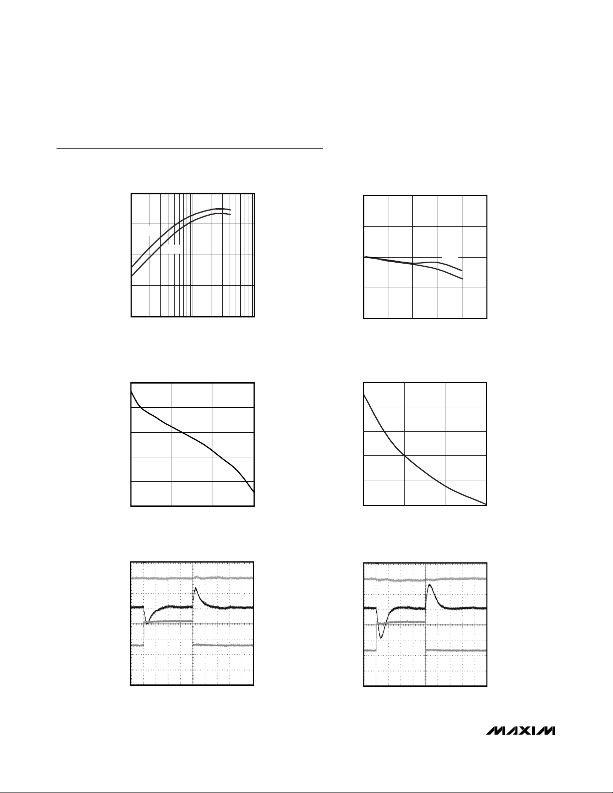
Typical Operating Characteristics
(Circuit of Figure 1, VIN= 6V, TA = +25°C, unless otherwise noted.)
EFFICIENCY vs. LOAD
MAX8529 toc01
LOAD (A)
EFFICIENCY (%)
10.1
10
20
30
40
50
60
70
80
90
100
0
10
OUT2
OUT1
OUTPUT VOLTAGE ACCURACY
vs. LOAD
MAX8529 toc02
LOAD (A)
OUTPUT VOLTAGE ACCURACY (%)
43
12
-0.5
0.5
0
1.0
-1.0
05
OUT2
OUT1
VL VOLTAGE ACCURACY
vs. LOAD CURRENT
MAX8529 toc03
LOAD CURRENT (mA)
V
L
VOLTAGE ACCURACY
10050
-1.5
-1.0
-0.5
0
0.5
-2.0
0150
SWITCHING FREQUENCY vs. R
OSC
MAX8529 toc04
R
OSC
(kΩ)
SWITCHING FREQUENCY (kHz)
86
800
1000
1200
1400
1600
600
410
LOAD TRANSIENT RESPONSE (OUTPUT 1)
MAX8529 toc05
10μs/div
0A
I
OUT1
1A/div
V
OUT1
50mV/div
AC-COUPLED
V
OUT2
50mV/div
AC-COUPLED
LOAD TRANSIENT RESPONSE (OUTPUT 2)
MAX8529 toc06
10μs/div
0A
I
OUT2
1A/div
V
OUT1
50mV/div
AC-COUPLED
V
OUT2
50mV/div
AC-COUPLED
Page 5
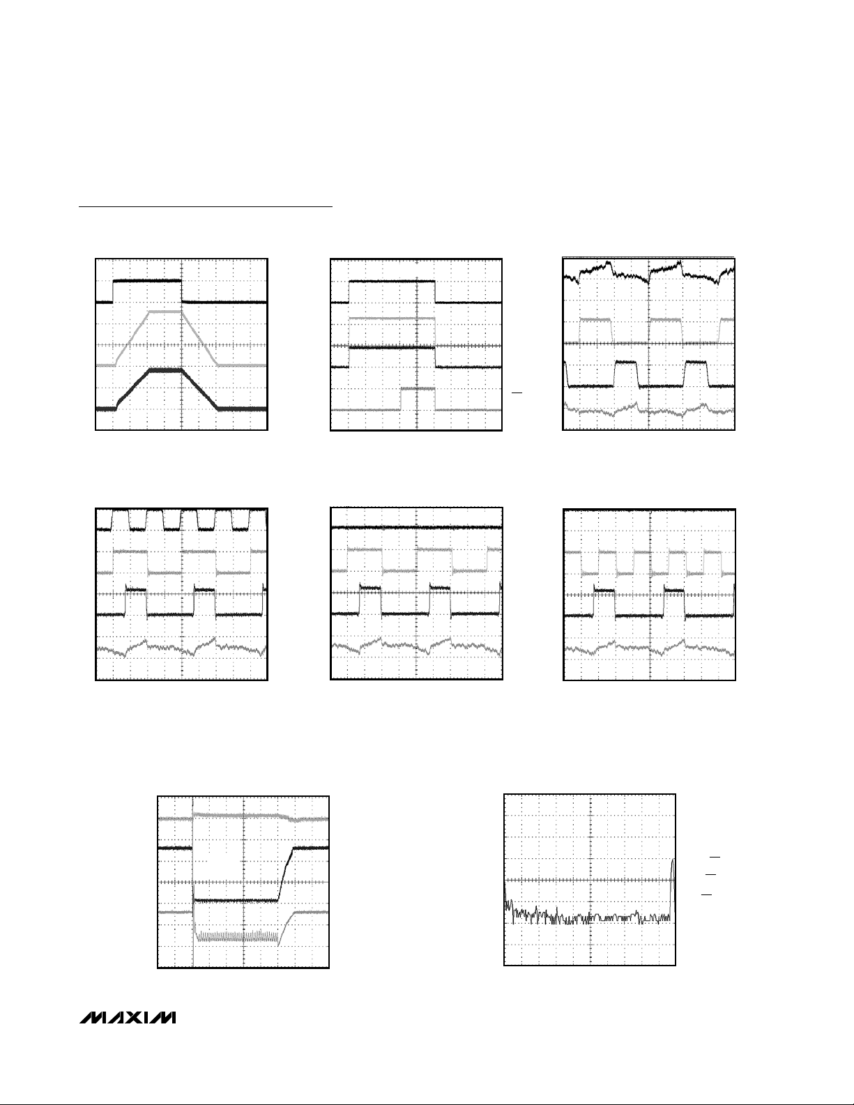
SOFT-START AND SOFT-STOP WAVEFORM
MAX8529 toc07
400μs/div
0V
0V
V
OUT2
1V/div
V
OUT1
1V/div
5V
0V
EN
RESET TIMEOUT
MAX8529 toc08
100ms/div
V
OUT1
2V/div
0V
0V
0V
V
OUT2
2V/div
0V
EN
5V
V
RST
5V/div
OUT-OF-PHASE WAVEFORM
MAX8529 toc09
200ns/div
V
OUT2
10mV/div
AC-COUPLED
V
OUT1
10mV/div
AC-COUPLED
V
LX2
5V/div
V
LX1
5V/div
0V
0V
MAX8529
1.5MHz Dual 180° Out-of-Phase
PWM Step-Down Controller with POR
_______________________________________________________________________________________ 5
Typical Operating Characteristics (continued)
(Circuit of Figure 1, VIN= 6V, TA = +25°C, unless otherwise noted.)
EXTERNALLY SYNCHRONIZED
SWITCHING WAVEFORM
200ns/div
MAX8529 toc10
5V
V
SYNC
0V
5V
V
CKO
0V
V
LX1
5V/div
0V
V
OUT1
10mV/div
AC-COUPLED
CKO OUTPUT WAVEFORM
200ns/div
MAX8529 toc11
SYNC = GND
5V
V
CK0
0V
V
LX1
5V/div
0V
V
OUT1
10mV/div
AC-COUPLED
CKO OUTPUT WAVEFORM
SYNC = V
200ns/div
MAX8529 toc12
L
5V
V
CK0
0V
V
LX1
5V/div
0V
V
OUT1
10mV/div
AC-COUPLED
SHORT-CIRCUIT CURRENT FOLDBACK
AND RECOVERY
SHORT
V
OUT2
200μs/div
MAX8529 toc13
V
OUT1
50mV/div
AC-COUPLED
V
OUT2
1V/div
0V
I
OUT2
2A/div
0A
OUTPUT2 NOISE SPECTRUM
0
250
500
FREQUENCY (kHz)
MAX8529 toc14
400nV/√Hz
40nV/√Hz
4nV/√Hz
750 1000 1250
Page 6

MAX8529
1.5MHz Dual 180° Out-of-Phase
PWM Step-Down Controller with POR
6 _______________________________________________________________________________________
Pin Description
PIN NAME FUNCTION
1 COMP2 Compensation Pin for Regulator 2 (REG2). Compensate REG2’s control loop as shown in Figure 1.
Feedback Input for Regulator 2 (REG2). Connect FB2 to a resistive-divider between REG2’s output
2 FB2
3 ILIM2
4 OSC
5 V+ Input Supply Voltage (4.75V to 23V)
6 REF 2V Reference Output. Bypass to GND with a 0.22µF or greater ceramic capacitor.
7 GND Analog Ground
8 CKO
9 SYNC
10 ILIM1
and GND to adjust the output voltage between 1V and 18V. To set the output voltage below 1V,
connect FB2 to a resistive voltage-divider from REF to REG2’s output (see the Setting the Output
Voltage section).
Current-Limit Adjustment for Regulator 2 (REG2). The PGND–LX2 current-limit threshold defaults to
100mV if ILIM2 is connected to V
REG2’s current-limit threshold (V
the Setting the Valley Current Limit section).
Oscillator Frequency Set Input. The controller generates the clock signal by dividing down the
oscillator, so the switching frequency equals half the synchronization frequency (f
Connect a resistor from OSC to GND (R
10kΩ) to 1500kHz (R
connected to SYNC. When using SYNC, set R
Clock Output. Clock Output for external 2- or 4-phase synchronization (see the Clock Synchronization
(SYNC, CKO) section).
Synchronization Input or Clock Output Selection Input. SYNC has three operating modes. Connect
SYNC to a 1200kHz to 2800kHz clock for external synchronization. Connect SYNC to GND for 2phase operation as a master controller. Connect SYNC to V
controller (see the Clock Synchronization (SYNC, CKO) section).
Current-Limit Adjustment for Regulator 1 (REG1). The PGND–LX1 current-limit threshold defaults to
100mV if ILIM1 is connected to V
current-limit threshold (V
Setting the Valley Current Limit section).
= 4kΩ). The controller still requires R
OSC
ITH1
. Connect a resistor (R
L
) from 50mV (R
ITH2
OSC
. Connect a resistor (R
L
) from 50mV (R
ILIM2
= 100kΩ) to 300mV (R
ILIM2
) to set the switching frequency from 600kHz (R
for one half of the SYNC input.
OSC
for 4-phase operation as a master
L
ILIM1
= 100kΩ) to 300mV (R
ILIM1
) from ILIM2 to GND to adjust the
= 600kΩ) (see
ILIM2
= f
OSC
/ 2).
OSC
=
SW
when an external clock is
OSC
) from ILIM1 to GND to adjust REG1’s
= 600kΩ) (see the
ILIM1
Feedback Input for Regulator 1 (REG1). Connect FB1 to a resistive-divider between REG1’s output
11 FB1
12 COMP1 Compensation Pin for Regulator 1 (REG1). Compensate REG1’s control loop as shown in Figure 1.
13 RST
and GND to adjust the output voltage between 1V and 18V. To set the output voltage below 1V,
connect FB1 to a resistive voltage-divider from REF and REG1’s output (see the Setting the Output
Voltage section).
Open-Drain Reset Output. RST is low when either output voltage is more than 10% below its
regulation point. After soft-start is completed and both outputs exceed 90% of their nominal output
voltage (VFB_ > 0.9V), RST becomes high impedance after a 140ms delay and remains high
impedance as long as both outputs maintain regulation. Connect a resistor between RST and the
logic supply for logic-level voltages.
Page 7
Detailed Description
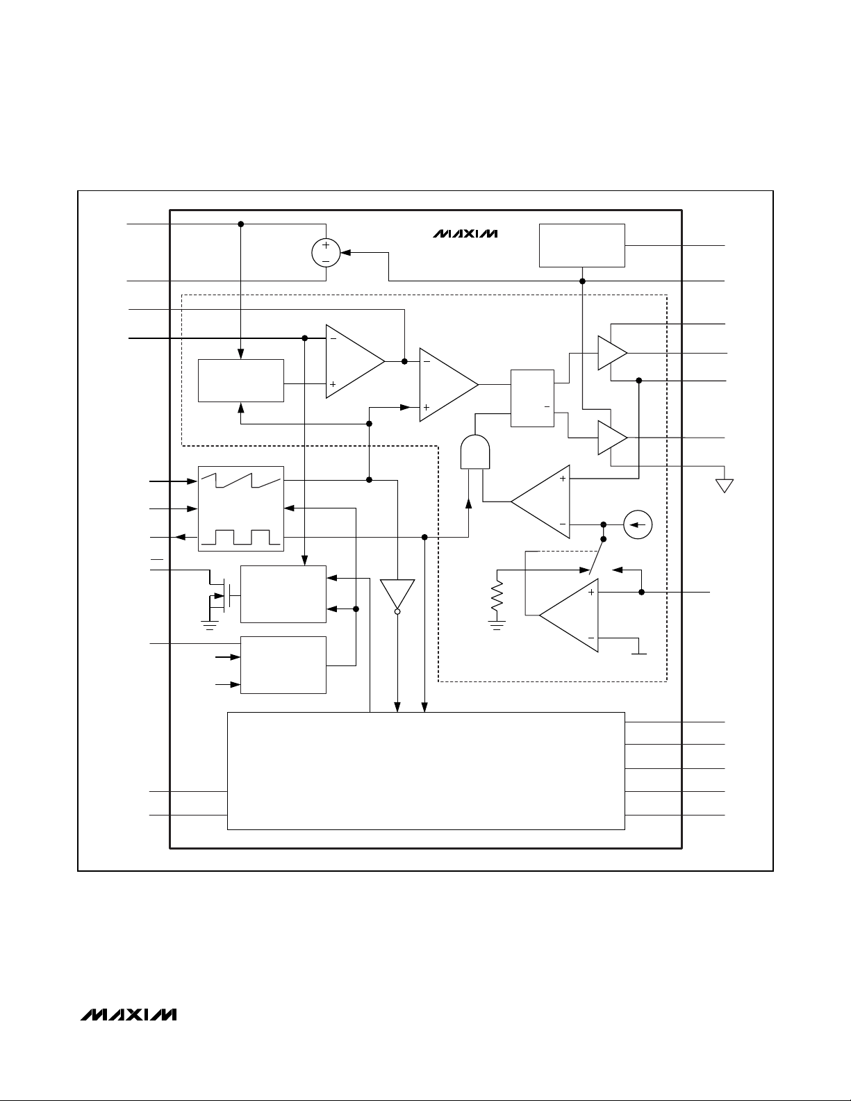
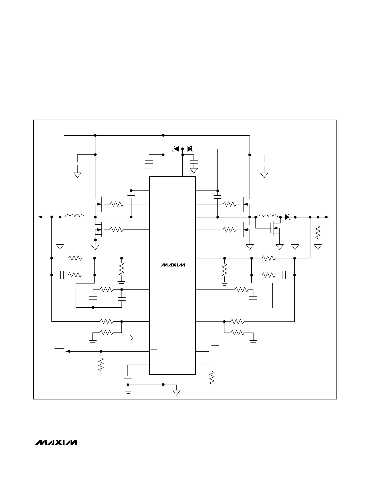
DC-to-DC PWM Controller
The MAX8529 step-down converter uses a PWM voltage-mode control scheme (Figure 2) for each out-ofphase controller. The controller generates the clock
signal by dividing down the internal oscillator or SYNC
input when driven by an external clock, so each controller’s switching frequency equals half the oscillator frequency (fSW= f
OSC
/ 2). An internal transconductance
error amplifier produces an integrated error voltage at
the COMP pin, providing high DC accuracy. The voltage
at COMP sets the duty cycle using a PWM comparator
and a ramp generator. At each rising edge of the clock,
REG1’s high-side n-channel MOSFET turns on and
remains on until either the appropriate duty cycle or until
the maximum duty cycle is reached. REG2 operates outof-phase, so the second high-side MOSFET turns on at
each falling edge of the clock. During each high-side
MOSFET’s on-time, the associated inductor current
ramps up.
During the second-half of the switching cycle, the highside MOSFET turns off and the low-side n-channel
MOSFET turns on. Now the inductor releases the stored
energy as its current ramps down, providing current to
the output. Under overload conditions, when the inductor current exceeds the selected valley current limit
(see the Current-Limit Circuit (ILIM_) section), the highside MOSFET does not turn on at the appropriate clock
edge and the low-side MOSFET remains on to let the
inductor current ramp down.
Synchronized Out-of-Phase Operation
The two independent regulators in the MAX8529 operate
180 degrees out-of-phase to reduce input filtering
requirements, reduce electromagnetic interference (EMI),
and improve efficiency. This effectively lowers component
cost and saves board space, making the MAX8529 ideal
for cost-sensitive applications.
Dual-switching regulators typically operate both
controllers in-phase, and turn on both high-side MOSFETs
at the same time. The input capacitor must then support
the instantaneous current requirements of both controllers
simultaneously, resulting in increased ripple voltage and
current when compared to a single switching regulator.
The higher RMS ripple current lowers efficiency due to
power loss associated with the input capacitor’s effective
series resistance (ESR). This typically requires more lowESR input capacitors in parallel to minimize input voltage
ripple and ESR-related losses, or to meet the necessary
ripple-current rating.
MAX8529
1.5MHz Dual 180° Out-of-Phase
PWM Step-Down Controller with POR
_______________________________________________________________________________________ 7
Pin Description (continued)
PIN NAME FUNCTION
14 DH1 High-Side Gate Driver Output for Regulator 1 (REG1). DH1 swings from LX1 to BST1.
15 LX1
16 BST1
17 DL1 Low-Side Gate-Driver Output for Regulator 1 (REG1). DL1 swings from PGND to VL.
18 PGND Power Ground
19 V
20 DL2 Low-Side Gate-Driver Output for Regulator 2 (REG2). DL2 swings from PGND to VL.
21 BST2
22 LX2
23 DH2 High-Side Gate-Driver Output for Regulator 2 (REG2). DH2 swings from LX2 to BST2.
24 EN
L
External Inductor Connection for Regulator 1 (REG1). Connect LX1 to the switched side of the
inductor. LX1 serves as the lower supply rail for the DH1 high-side gate driver.
Boost Flying-Capacitor Connection for Regulator 1 (REG1). Connect BST1 to an external ceramic
capacitor and diode according to Figure 1.
Internal 5V Linear-Regulator Output. Supplies the regulators and powers the low-side gate drivers
and external boost circuitry for the high-side gate drivers.
Boost Flying-Capacitor Connection for Regulator 2 (REG2). Connect BST2 to an external ceramic
capacitor and diode according to Figure 1.
External Inductor Connection for Regulator 2 (REG2). Connect LX2 to the switched side of the
inductor. LX2 serves as the lower supply rail for the DH2 high-side gate driver.
Active-High Enable Input. A logic low shuts down both controllers. Connect to V
operation.
for always-on
L
Page 8

MAX8529
With dual synchronized out-of-phase operation, the
MAX8529’s high-side MOSFETs turn on 180 degrees outof-phase. The instantaneous input current peaks of both
regulators no longer overlap, resulting in reduced RMS
ripple current and input voltage ripple. This reduces the
required input capacitor ripple-current rating, allowing
fewer or less expensive capacitors, and reduces shielding requirements for EMI. The out-of-phase waveforms in
the Typical Operating Characteristics demonstrate syn-
chronized 180-degree out-of-phase operation.
Internal 5V Linear Regulator (VL)
All MAX8529 functions are internally powered from an
on-chip, low-dropout 5V regulator. The maximum regulator input voltage (V+) is 23V. Bypass the regulator’s
output (V
L
) with a 4.7µF ceramic capacitor to PGND.
The VLdropout voltage is typically 500mV, so when V+
is greater than 5.5V, VLis typically 5V. The MAX8529
also employs an undervoltage lockout circuit that disables both regulators when VLfalls below 4.5V.
1.5MHz Dual 180° Out-of-Phase
PWM Step-Down Controller with POR
8 _______________________________________________________________________________________
Figure 1. Standard Application Circuit
5.4V TO 6.6V
V
IN
D1A, B
CMPSH-3A
C2
10μF
10V
X5R
(2x)
1.8V AT
3A
V
OUT1
C1
22μF
6V
X5R
(2x)
C4
390pF
L1
1.0μH
DO3316P
-102HC
R3
16.5kΩ
R5
560Ω
N1A, B
FDS
6912A
C5
1nF
R6
10kΩ
3.3Ω
3.3Ω
20.5kΩ
C6
27pF
R1
R2
R4
0.22μF
10V
C3
0.1μF
C8
5
19
16
14
15
17
18
11
12
IN
BST1
DH1
LX1
DL1
PGND
FB1
COMP1
U1
MAX8529
V
L
COMP2
BST2
DH2
LX2
DL2
FB2
C9
4.7μF
10V
X5R
21
C10
0.1μF
23
22
20
2
1
R10
3.3Ω
R11
3.3Ω
R13
11.0kΩ
C14
10pF
R15
10kΩ
N2A, B
FDS
6912A
16.5kΩ
C5
1nF
L2
1.5μH
DO3316P
-152HC
22μF
R12
R14
560Ω
C12
X5R
(2x)
C11
10μF
10V
X5R
(2x)
6V
C13
390pF
2.5V AT
3A
V
OUT2
R7
RESET
100kΩ
22kΩ
R8
68kΩ
R9
V
L
0.22μF
V
C7
10
ILIM1
24
L
EN
13
RST
6
REF
GND
7
R16
R18
4.99kΩ
68kΩ
R17
68kΩ
ILIM2
SYNC
CKO
OSC
3
9
8
4
Page 9
The internal VLlinear regulator can source over 50mA to
supply the IC, power the low-side gate driver, charge the
external boost capacitor, and supply small external
loads. When driving large FETs, little or no regulator current may be available for external loads.
For example, when switched at 600kHz, a single large
FET with 18nC total gate charge requires 18nC ✕600kHz
= 11mA. To drive larger MOSFETs, or deliver larger
loads, connect VLto an external power supply from
4.75V to 5.5V.
MAX8529
1.5MHz Dual 180° Out-of-Phase
PWM Step-Down Controller with POR
_______________________________________________________________________________________ 9
REF
Figure 2. Functional Diagram
GND
COMP1
FB1
OSC
V+
V
L
BST1
DH1
LX1
DL1
PGND
SOFT-START
DAC
V
2.0V
Q
Q
5V LINEAR
REGULATOR
REF
g
m
MAX8529
CONVERTER 1
R
S
SYNC
CK0
RST
EN
V
REF
V
L
COMP2
OSCILLATOR
RESET
UVLO
AND
SHUTDOWN
CONVERTER 2
V
5μA
- 0.5V
L
ILIM1
BST2
DH2
LX2
DL2
ILIM2FB2
Page 10

MAX8529
High-Side Gate-Drive Supply (BST_)
Gate-drive voltages for the high-side n-channel switches are generated by the flying-capacitor boost circuits
(Figure 3). A boost capacitor (connected from BST_ to
LX_) provides power to the high-side MOSFET driver.
On startup, the synchronous rectifier (low-side MOSFET)
forces LX_ to ground and charges the boost capacitor to
5V. On the second half-cycle, after the low-side MOSFET
turns off, the high-side MOSFET is turned on by closing
an internal switch between BST_ and DH_. This provides
the necessary gate-to-source voltage to turn on the highside switch, an action that boosts the 5V gate-drive
signal above V
IN
. The current required to drive the high-
side MOSFET gates (f
SWITCH
✕
QG) is ultimately drawn
from V
L
.
MOSFET Gate Drivers (DH_, DL_)
The DH and DL drivers are optimized for driving
moderate-size n-channel high-side and larger low-side
power MOSFETs. This is consistent with the low duty
factor seen with a large V
IN
- V
OUT
differential. The DL_
low-side drive waveform is always the complement of
the DH_ high-side drive waveform (with controlled dead
time to prevent cross-conduction or “shoot-through”).
An adaptive dead-time circuit monitors the DL_ output
and prevents the high-side FET from turning on until
DL_ is fully off. There must be a low-resistance, lowinductance path from the DL_ driver to the MOSFET
gate in order for the adaptive dead-time circuit to work
properly. Otherwise, the sense circuitry in the MAX8529
interprets the MOSFET gate as “off” while there is actually charge still left on the gate. Use very short, wide
traces (50mils to 100mils wide if the MOSFET is 1in
from the device). The dead time at the DH off edge is
determined by a fixed 30ns internal delay.
Synchronous rectification reduces conduction losses in
the rectifier by replacing the normal low-side Schottky
catch diode with a low-resistance MOSFET switch.
Additionally, the MAX8529 uses the synchronous rectifier to ensure proper startup of the boost gate-driver circuit and to provide the current-limit signal.
The internal pulldown transistor that drives DL_ low is
robust, with a 0.5Ω (typ) on-resistance. This low onresistance helps prevent DL_ from being pulled up during the fast rise-time of the LX_ node, due to capacitive
coupling from the drain to the gate of the low-side synchronous-rectifier MOSFET. However, for high-current
applications, some combinations of high- and low-side
FETs can cause excessive gate-drain coupling, leading
to poor efficiency, EMI, and shoot-through currents.
This can be remedied by adding a resistor (typically
less than 5Ω) in series with BST_, which increases the
turn-on time of the high-side FET without degrading the
turn-off time (Figure 3).
Current-Limit Circuit (ILIM_)
The current-limit circuit employs a “valley” current-sensing algorithm that uses the on-resistance of the low-side
MOSFET as a current-sensing element. If the currentsense signal is above the current-limit threshold, the
MAX8529 does not initiate a new cycle (Figure 4). Since
valley current sensing is employed, the actual peak current is greater than the current-limit threshold by an
amount equal to the inductor ripple current. Therefore,
the exact current-limit characteristic and maximum load
capability are a function of the low-side MOSFET’s onresistance, current-limit threshold, inductor value, and
input voltage. The reward for this uncertainty is robust,
lossless overcurrent sensing that does not require costly
sense resistors.
The adjustable current limit accommodates MOSFETs
with a wide range of on-resistance characteristics (see
the Design Procedure section). The current-limit
threshold is adjusted with an external resistor at ILIM_
(Figure 1). The adjustment range is from 50mV to
300mV, corresponding to resistor values of 100kΩ to
1.5MHz Dual 180° Out-of-Phase
PWM Step-Down Controller with POR
10 ______________________________________________________________________________________
Figure 3. Reducing the Switching-Node Rise Time
Figure 4. “Valley” Current-Limit Threshold Point
INPUT
)
(V
V
L
BST_
DH_
LX_
MAX8529
INDUCTOR CURRENT
0 TIME
5Ω
IN
I
PEAK
I
LOAD
I
LIMIT
Page 11

600kΩ. In adjustable mode, the current-limit threshold
across the low-side MOSFET is precisely 1/10th the
voltage seen at ILIM_. However, the current-limit
threshold defaults to 100mV when ILIM is connected to
V
L
. The logic threshold for switchover to this 100mV
default value is approximately V
L
- 0.5V.
Adjustable foldback current limit reduces power dissipation during short-circuit conditions (see the Design
Procedure section).
Carefully observe the PC board layout guidelines to
ensure that noise and DC errors do not corrupt the current-sense signals seen by LX_ and PGND. The IC
must be mounted close to the low-side MOSFET with
short direct traces making a Kelvin sense connection
so that trace resistance does not add to the intended
sense resistance of the low-side MOSFET.
Undervoltage Lockout and Startup
If VLdrops below 4.5V, the MAX8529 assumes that the
supply and reference voltages are too low to make valid
decisions and activates the undervoltage lockout (UVLO)
circuitry, which forces DH low and DL high to inhibit
switching. RST is also forced low during UVLO. After V
L
rises above 4.5V, the controller powers up the outputs.
Enable (EN), Soft-Start, and Soft-Stop
Pull EN high to enable or low to shut down both regulators. During shutdown the supply current drops to 1mA
(max), LX enters a high-impedance state (DH_ connected to LX_, and DL_ connected to PGND), and
COMP_ is discharged to GND through a 17Ω resistor.
V
L
and REF remain active in shutdown. For “always-on”
operation, connect EN to V
L
.
On the rising edge of EN both controllers enter softstart. Soft-start gradually ramps up to the reference
voltage seen by the error amplifier in order to control
the outputs’ rate of rise and reduce input surge currents during startup. The soft-start period is 1024 clock
cycles (1024/fSW), and the internal soft-start DAC
ramps up the voltage in 64 steps. The output reaches
regulation when soft-start is completed. On the falling
edge of EN both controllers simultaneously enter softstop, which reverses the soft-start ramp. The part
enters shutdown after soft-stop is complete.
Reset Output
RST is an open-drain output. RST pulls low when either
output falls below 90% of its nominal regulation voltage.
Once both outputs exceed 90% of their nominal regulation
voltages and both soft-start cycles are completed, RST
goes high impedance. To obtain a logic-voltage output,
connect a pullup resistor from RST to the logic supply
voltage. A 100kΩ resistor works well for most applications.
If unused, leave RST grounded or unconnected.
Clock Synchronization (SYNC, CKO)
SYNC serves two functions: SYNC selects the clock
output (CKO) type used to synchronize slave controllers, or it serves as a clock input so the MAX8529
can be synchronized with an external clock signal. This
allows the MAX8529 to function as either a master or
slave. CKO provides a clock signal synchronized to the
MAX8529’s switching frequency, allowing either inphase (SYNC = GND) or 90-degrees out-of-phase
(SYNC = VL) synchronization of additional DC-to-DC
controllers (Figure 5). The MAX8529 supports the following three operating modes:
• SYNC = GND: The CKO output frequency equals
REG1’s switching frequency (f
CKO
= f
DH1
) and the
CKO signal is in phase with REG1’s switching frequency. This provides 2-phase operation when synchronized with a second slave controller.
• SYNC = VL: The CKO output frequency equals two
times REG1’s switching frequency (f
CKO
= 2f
DH1
)
and the CKO signal is phase shifted by 90 degrees
with respect to REG1’s switching frequency. This
provides 4-phase operation when synchronized with
a second MAX8529 (slave controller).
• SYNC Driven by External Oscillator: The controller
generates the clock signal by dividing down the
SYNC input signal, so that the switching frequency
equals half the synchronization frequency (fSW=
f
SYNC
/ 2). REG1’s conversion cycles initiate on the
rising edge of the internal clock signal. The CKO output frequency and phase match REG1’s switching
frequency (f
CKO
= f
DH1
) and the CKO signal is in
phase. Note that the MAX8529 still requires R
OSC
when SYNC is externally clocked and the internal
oscillator frequency should be set to 50% of the synchronization frequency (f
OSC
= 0.5 f
SYNC
).
Thermal-Overload Protection
Thermal-overload protection limits total power dissipation
in the MAX8529. When the device’s die junction temperature exceeds TJ= +160°C, an on-chip thermal sensor
shuts down the device, forcing DL_ and DH_ low, allowing the IC to cool. The thermal sensor turns the part on
again after the junction temperature cools by 10°C.
During thermal shutdown, the regulators shut down, RST
goes low, and soft-start is reset. If the VLlinear-regulator
output is short-circuited, thermal-overload protection is
triggered.
MAX8529
1.5MHz Dual 180° Out-of-Phase
PWM Step-Down Controller with POR
______________________________________________________________________________________ 11
Page 12

MAX8529
Design Procedure
Effective Input Voltage Range
Although the MAX8529 controllers can operate from
input supplies ranging from 4.75V to 23V, the input
voltage range can be effectively limited by the
MAX8529’s duty-cycle limitations. The maximum input
voltage is limited by the minimum on-time (t
ON(MIN)
):
where t
ON(MIN)
is 100ns. The minimum input voltage is
limited by the maximum duty cycle (D
MAX
= 0.875):
where V
DROP1
is the sum of the parasitic voltage drops in
the inductor discharge path, including synchronous rectifier, inductor, and PCB resistances. V
DROP2
is the sum of
the resistances in the charging path, including high-side
switch, inductor, and PCB resistances.
Setting the Switching Frequency
The controller generates the clock signal by dividing
down the internal oscillator or SYNC input signal when
driven by an external oscillator, so the switching
frequency equals half the oscillator frequency (fSW=
f
OSC
/2). The internal oscillator frequency is set by a
resistor (R
OSC
) connected from OSC to GND. The rela-
tionship between fSWand R
OSC
is:
where fSWis in Hz, f
OSC
is in Hz, and R
OSC
is in Ω. For
example, a 600kHz switching frequency is set with
R
OSC
= 10kΩ. Higher frequencies allow designs with
lower inductor values and less output capacitance.
Consequently, peak currents and I2R losses are lower
at higher switching frequencies, but core losses, gatecharge currents, and switching losses increase.
A rising clock edge on SYNC is interpreted as a synchronization input. If the SYNC signal is lost, the internal
oscillator takes control of the switching rate, returning
the switching frequency to that set by R
OSC
. This maintains output regulation even with intermittent SYNC signals. When an external synchronization signal is used,
R
OSC
should set the switching frequency to one half
SYNC rate (f
SYNC
).
R
Hz
S
f
OSC
SW
=×
610
9
Ω -
V
VV
VV
IN MIN
OUT DROP
DROP DROP()
.
=
+
⎡
⎣
⎢
⎤
⎦
⎥
+
1
21
0 875
-
V
V
tf
IN MAX
OUT
ON MIN SW
()
()
≤
1.5MHz Dual 180° Out-of-Phase
PWM Step-Down Controller with POR
12 ______________________________________________________________________________________
Figure 5. Synchronized Controllers
MAX8529 MAX8529
OSC
MASTER
180° PHASE SHIFT 90° PHASE SHIFT
SLAVE
DH1
DH2
DH1
DH2
MASTER
CK0
SYNC
V
L
SYNC
SLAVE
MAX8529 MAX8529
OSC OSC
MASTER
MASTER
SLAVE
DH1
DH2
DH1
DH2
CK0
SYNC
V
L
4-PHASE SYSTEM2-PHASE SYSTEM
SYNC
SLAVE
Page 13

Inductor Selection
Three key inductor parameters must be specified for
operation with the MAX8529: inductance value (L),
peak-inductor current (I
PEAK
), and DC resistance (RDC).
The following equation assumes a constant ratio of
inductor peak-to-peak AC current to DC average current
(LIR). For LIR values too high, the RMS currents are
high, and therefore I2R losses are high. Large inductances must be used to achieve very low LIR values.
Typically inductance is proportional to resistance (for a
given package type), which again makes I
2
R losses
high for very low LIR values. A good compromise
between size and loss is a 30% peak-to-peak ripple current to average-current ratio (LIR = 0.3). The switching
frequency, input voltage, output voltage, and selected
LIR determine the inductor value as follows:
where VIN, V
OUT
, and I
OUT
are typical values (so that efficiency is optimum for typical conditions). The switching
frequency is set by R
OSC
(see the Setting the Switching
Frequency section). The exact inductor value is not
critical and can be adjusted in order to make trade-offs
among size, cost, and efficiency. Lower inductor values
minimize size and cost, but also improve transient
response and reduce efficiency due to higher peak currents. On the other hand, higher inductance increases
efficiency by reducing the RMS current. However, resistive losses due to extra wire turns can exceed the benefit
gained from lower AC current levels, especially when the
inductance is increased without also allowing larger
inductor dimensions.
Find a low-loss inductor having the lowest possible DC
resistance that fits in the allotted dimensions. The
inductor’s saturation rating must exceed the peakinductor current at the maximum defined load current
(I
LOAD(MAX)
):
Setting the Valley Current Limit
The minimum current-limit threshold must be high
enough to support the maximum expected load current
with the worst-case low-side MOSFET on-resistance
value since the low-side MOSFET’s on-resistance is used
as the current-sense element. The inductor’s valley current occurs at I
LOAD(MAX)
minus half of the ripple cur-
rent. The current-sense threshold voltage (V
ITH
) should
be greater than the voltage on the low-side MOSFET
during the ripple-current valley:
where R
DS(ON)
is the on-resistance of the low-side
MOSFET (N
L
). Use the maximum value for R
DS(ON)
from the low-side MOSFET’s data sheet, an additional
margin to account for R
DS(ON)
rise with temperature is
also recommended. A good general rule is to allow
0.5% additional resistance for each °C of the MOSFET
junction temperature rise.
Connect ILIM_ to VLfor the default 100mV (typ) currentlimit threshold. For an adjustable threshold, connect a
resistor (R
ILIM
_) from ILIM_ to GND. The relationship
between the current-limit threshold (V
ITH
_) and R
ILIM
_ is:
where R
ILIM
_ is in Ω and V
ITH
_ is in V.
An R
ILIM
resistance range of 100kΩ to 600kΩ corre-
sponds to a current-limit threshold of 50mV to 300mV.
When adjusting the current limit, 1% tolerance resistors
minimize error in the current-limit threshold.
For foldback current limit, a resistor (R
FBI
) is added
from ILIM pin to output. The value of R
ILIM
and R
FBI
can then be calculated as follows:
First select the percentage of foldback, PFB, from 15%
to 30%, then:
Input Capacitor
The input filter capacitor reduces peak currents drawn
from the power source and reduces noise and voltage
ripple on the input caused by the circuit’s switching.
The input capacitor must meet the ripple current
requirement (I
RMS
) imposed by the switching currents
as defined by the following equation:
I
RMS
has a maximum value when the input voltage equals
twice the output voltage (VIN= 2V
OUT
), so I
RMS(MAX)
=
I
LOAD
/ 2. For most applications, nontantalum capacitors
II
VVV
V
RMS LOAD
OUT IN OUT
IN
=
() -
R
PV
P
and
R
VPR
VVP
FBI
FB OUT
FB
ILIM
ITH FB FBI
OUT ITH FB
=
×
×
=
××
×
[]
( )
( )
( )
5101
10 1
10 1
6-
-
-
- -
R
V
A
ILIM
ITH__
.=
μ05
VR I
LIR
ITH DS ON MAX LOAD MAX
>××
⎛
⎝
⎜
⎞
⎠
⎟
(, ) ( )
12-
II
LIR
I
PEAK LOAD MAX LOAD MAX
=+
⎛
⎝
⎜
⎞
⎠
⎟
() ()
2
L
VVV
V f I LIR
OUT IN OUT
IN SW OUT
()
=
-
MAX8529
1.5MHz Dual 180° Out-of-Phase
PWM Step-Down Controller with POR
______________________________________________________________________________________ 13
Page 14

MAX8529
(ceramic, aluminum, polymer, or OS-CON) are preferred
at the input due to their robustness with high inrush currents typical of systems that can be powered from very
low impedance sources. Additionally, two (or more)
smaller-value low-ESR capacitors can be connected in
parallel for lower cost. Choose an input capacitor that
exhibits less than 10°C temperature rise at the RMS input
current for optimal long-term reliability.
Output Capacitor
The key selection parameters for the output capacitor
are capacitance value, ESR, and voltage rating. These
parameters affect the overall stability, output ripple voltage, and transient response. The output ripple has two
components: variations in the charge stored in the output capacitor, and the voltage drop across the capacitor’s ESR caused by the current flowing into and out of
the capacitor:
The output voltage ripple as a consequence of the ESR
and output capacitance is:
where I
P-P
is the peak-to-peak inductor current (see the
Inductor Selection section). These equations are suitable
for initial capacitor selection, but final values should be
verified by testing in a prototype or evaluation circuit.
As a general rule, a smaller inductor ripple current results
in less output ripple voltage. Since inductor ripple current
depends on the inductor value and input voltage, the output ripple voltage decreases with larger inductance and
increases with higher input voltages. However, the inductor ripple current also impacts transient-response performance, especially at low VIN- V
OUT
differentials. Low
inductor values allow the inductor current to slew faster,
replenishing charge removed from the output filter capacitors by a sudden load step. The amount of output-voltage sag is also a function of the maximum duty factor,
which can be calculated from the minimum off-time and
switching frequency:
where t
OFF(MIN)
is the minimum off-time (see the
Electrical Characteristics), and fSWis set by R
OSC
(see
the Setting the Switching Frequency section).
Compensation
The high switching frequency range of the MAX8529
allows the use of ceramic output capacitors. Since the
ESR of ceramic capacitors is typically very low, the frequency of the associated transfer function zero is higher
than the unity-gain crossover frequency and the zero cannot be used to compensate for the double pole created
by the output inductor and capacitor. The solution is Type
3 compensation which takes advantage of local feedback
to create two zeros and three poles (Figure 6). The frequency of the poles and zeros are described below:
V
LI I
V
Vf
t
CV
VV
Vf
t
SAG
LOAD LOAD
OUT
IN SW
OFF MIN
OUT OUT
IN OUT
IN SW
OFF MIN
=
⎛
⎝
⎜
⎞
⎠
⎟
+
⎡
⎣
⎢
⎢
⎤
⎦
⎥
⎥
⎛
⎝
⎜
⎞
⎠
⎟
⎡
⎣
⎢
⎢
⎤
⎦
⎥
⎥
()
()
()
12
2
2
-
-
-
VIR
V
I
Cf
I
VV
fLVV
RIPPLE ESR P P ESR
RIPPLE C
PP
OUT SW
PP
IN OUTSWOUT
IN
()
()
=
=
=
⎛
⎝
⎜
⎞
⎠
⎟
⎛
⎝
⎜
⎞
⎠
⎟
-
-
-
-
8
VV V
RIPPLE RIPPLE ESR RIPPLE C
() ()
≅+
1.5MHz Dual 180° Out-of-Phase
PWM Step-Down Controller with POR
14 ______________________________________________________________________________________
Figure 6. Compensation Network and Asymptotic Transfer Function
V
IN
DH
LX
L
O
GAIN (dB)
V
OUT
DL
MAX8529
FB
COMP
R4
C2
C
O
R3
C3
R2
R1
C1
fp1
fz1 fz2 fp2
fp3
FREQUENCY
Page 15
Unity-gain crossover frequency:
where:
V
IN,MAX
= Maximum input voltage
V
OSC
= Oscillator ramp voltage = 1V
LO= Output inductance
CO= Output capacitance
The goal is to place the two zeros below crossover and
the two poles above crossover so that crossover
occurs with a single-pole slope. The compensation procedure is as follows:
1) Select the crossover frequency such that:
2) Select R1 such that:
3) Place the first zero before the double pole:
4) Place the third pole at 1/2 the switching frequency:
C2 < 10pF can be omitted.
6) Place the second pole afer the ESR zero:
7) Place the second zero at the double pole frequency:
8) See the Setting the Output Voltage section for
selecting R4.
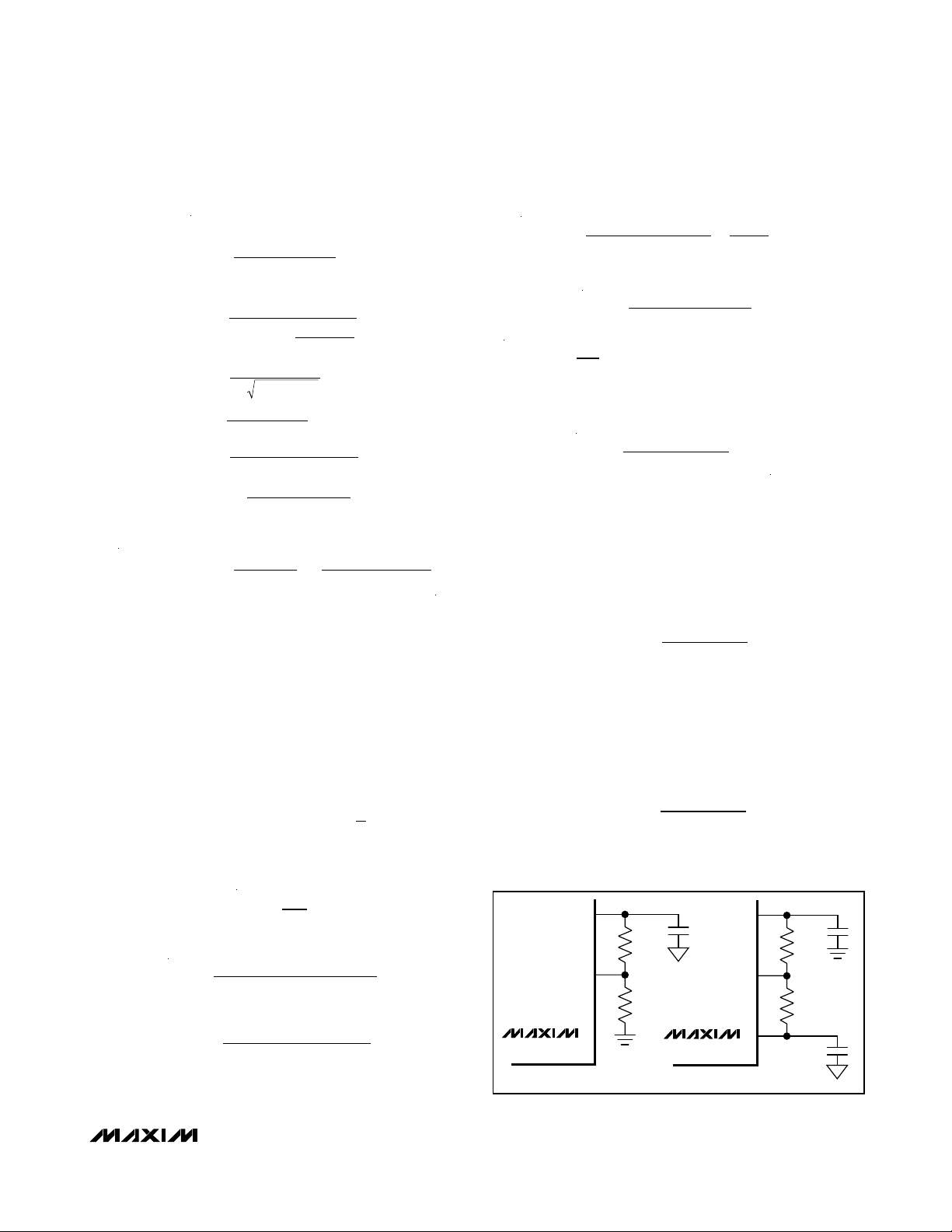
Setting the Output Voltage
For 1V or greater output voltages, set the MAX8529 output voltage by connecting a voltage-divider from the
output to FB_ to GND (Figure 7). Calculate R4 (OUT_ to
FB_ resistor) with the following equation:
where VSET = 1V (see the Electrical Characteristics)
and VOUT can range from VSET to 18V.
For output voltages below 1V, set the MAX8529 output
voltage by connecting a voltage-divider from the output
to FB_ to REF (Figure 7). Calculate R4 (FB_ to REF
resistor) with the following equation:
where VSET = 1V, VREF = 2V (see the Electrical
Characteristics), and VOUT can range from 0 to VSET.
RR
VV
VV
REF SET
SET OUT
43=
−
−
[]
R
fC
R
LC
3
1
23
2
≥
××π
-
If R
g
increase R and go back
to step
m
,
.
2
1
550 1
2
<=
()
Ω
R
fC
ZESR
2
1
23
≤
××π
53
2
1
0
)
C
fL CRV
V
O O OSC
IN
≤
×× ×
×
π
C
fR
S
2
1
205 1
.
≤
×
()
××π
C
fR
LC
1
1
2 0 75 1
.
≥
×
()
××π
R
g
m
12 >
f f and f f
f switching frequency
ZESR S
S
00
1
5
<<×
=
fRC
V
VLC
VINMAX
OO
OSC
0
13
1
2
=× × ×
××
,
π
f
f
RC
f
f
f
f
P
P
P
R
CC
CC
LC
LC
Z
RC
Z
RR
OO
1
2
3
1
21
12
12
1
2
1
1
211
2
1
223
0
1
223
=
=
××
=
××
×
()
+
()
=
×
=
××
=
×+
()
π
π
π
π
π
××
=
××
C
ZESR
RC
f
ESR O
3
1
2π
MAX8529
1.5MHz Dual 180° Out-of-Phase
PWM Step-Down Controller with POR
______________________________________________________________________________________ 15
Figure 7. Adjustable Output Voltage
V
RR
43=
SET
[]
−
VV
OUT SET
OUT_
R3
FB_
R4
MAX8529
V
> 1V
OUT_
MAX8529
REF
FB_
V
OUT_
R4
R3
OUT_
< 1V
Page 16

MAX8529
MOSFET Selection
The MAX8529’s step-down controller drives two external logic-level n-channel MOSFETs as the circuit switch
elements. The key selection parameters are:
• On-resistance (R
DS(ON)
)
• Maximum drain-to-source voltage (V
DS(MAX)
)
• Minimum threshold voltage (V
TH(MIN)
)
• Total gate charge (Q
g
)
• Reverse transfer capacitance (C
RSS
)
• Power dissipation
All four n-channel MOSFETs must be a logic-level type
with guaranteed on-resistance specifications at VGS≥
4.5V. For maximum efficiency, choose a high-side
MOSFET (NH_) that has conduction losses equal to the
switching losses at the optimum input voltage. Check to
ensure that the conduction losses at minimum input
voltage do not exceed MOSFET package thermal limits,
or violate the overall thermal budget. Also, check to
ensure that the conduction losses plus switching losses
at the maximum input voltage do not exceed package
ratings or violate the overall thermal budget.
Ensure that the MAX8529 DL_ gate drivers can drive
N
L
_. In particular, check that the dv/dt caused by NH_
turning on does not pull up the NL_ gate through NL_’s
drain-to-gate capacitance. This is the most frequent
cause of cross-conduction problems.
Gate-charge losses are dissipated by the driver and do
not heat the MOSFET. All MOSFETs must be selected
so that their total gate charge is low enough that VLcan
power all four drivers without overheating the IC:
MOSFET package power dissipation often becomes a
dominant design factor. I2R power losses are the greatest heat contributor for both high-side and low-side
MOSFETs. I2R losses are distributed between NH_ and
NL_ according to duty factor as shown in the equations
below. Switching losses affect only the high-side
MOSFET, since the low-side MOSFET is a zero-voltage
switched device when used in the buck topology.
Calculate MOSFET temperature rise according to package thermal-resistance specifications to ensure that
both MOSFETs are within their maximum junction temperature at high ambient temperature. The worst-case
dissipation for the high-side MOSFET (P
NH
) occurs at
both extremes of input voltage, and the worst-case dissipation for the low-side MOSFET (P
NL
) occurs at maxi-
mum input voltage:
I
GATE
is the average DH driver output current capability
determined by:
where R
DS(ON)DH
is the high-side MOSFET driver’s on-
resistance (5Ω max), and R
GATE
is any series resis-
tance between DH and BST (Figure 3).
where P
NH(CONDUCTION)
is the conduction power loss
in the high-side MOSFET, and PNLis the total low-side
power loss.
To reduce EMI caused by switching noise, add a 0.1µF
ceramic capacitor from the high-side switch drain to
the low-side switch source or add resistors in series
with DL_ and DH_ to increase the MOSFETs’ turn-on
and turn-off times.
Applications Information
Independent Shutdown
The two controllers in the MAX8529 can be shut down
independently by pulling COMP to ground. DH is
forced low and DL is forced high to inhibit switching.
Digital soft-stop is not active when using this method
for shutdown and the output voltage can go negative.
Use a Schottky clamp diode to limit the negative swing
of the output voltage.
When COMP is released, DH and DL resume switching.
In this mode, digital soft-start is not active and the
inrush current is limited by the foldback current limit.
Dropout Performance
When working with low input voltages, the output voltage
adjustable range for continuous-conduction operation is
restricted by the minimum off-time (t
OFF(MIN)
). For best
dropout performance, use the lowest (600kHz) switchingfrequency setting. Manufacturing tolerances and internal
propagation delays introduce an error to the switching
frequency and minimum off-time specifications. This error
is more significant at higher frequencies. Also, keep in
PIR
V
V
PP P
PI R
V
V
NH CONDUCTION LOAD DS ON NH
OUT
IN
NH TOTAL NH SWITCHING NH CONDUCTION
NL LOAD DS ON NL
OUT
IN
() ()
() ( )( )
()
=
⎛
⎝
⎜
⎞
⎠
⎟
=+
=
⎛
⎝
⎜
⎞
⎠
⎟
⎛
⎝
⎜
⎞
⎠
⎟
2
2
1-
I
V
RR
GATE
L
DS ON DH GATE
=
+
()
()
2
P
VI f Q Q
I
NH SWITCHING
IN LOAD OSC GS GD
GATE
()
=+
⎛
⎝
⎜
⎞
⎠
⎟
2
PV Q f
VL IN G TOTAL SW
=× ×
_
1.5MHz Dual 180° Out-of-Phase
PWM Step-Down Controller with POR
16 ______________________________________________________________________________________
Page 17

mind that transient response performance of buck regulators operated close to dropout is poor, and bulk output
capacitance must often be added (see the V
SAG
equa-
tion in the Design Procedure section).
The absolute point of dropout is when the inductor current ramps down during the minimum off-time (ΔI
DOWN
)
as much as it ramps up during the maximum on-time
(ΔIUP). The ratio h = ΔI
UP
/ ΔI
DOWN
is an indicator of
the ability to slew the inductor current higher in
response to increased load, and must always be
greater than 1. As h approaches 1, the absolute minimum dropout point, the inductor current cannot
increase as much during each switching cycle and
V
SAG
greatly increases unless additional output capac-
itance is used.
A reasonable minimum value for h is 1.5, but adjusting
this up or down allows tradeoffs between V
SAG
, output
capacitance, and minimum operating voltage.
For a given value of h, the minimum operating voltage
can be calculated as:
where V
DROP1
is the sum of the parasitic voltage drops
in the inductor discharge path, including synchronous
rectifier, inductor, and PCB resistances; V
DROP2
is the
sum of the resistances in the charging path, including
high-side switch, inductor, and PCB resistances; and
t
OFF(MIN)
is from the Electrical Characteristics. The
absolute minimum input voltage is calculated with h = 1.
If the calculated V+
(MIN)
is greater than the required minimum input voltage, then reduce the operating frequency
or add output capacitance to obtain an acceptable
V
SAG
. If operation near dropout is anticipated, calculate
V
SAG
to be sure of adequate transient response.
Dropout Design Example:
V
OUT
= 5V
fSW= 600kHz
t
OFF(MIN)
= 250ns
V
DROP1
= V
DROP2
= 100mV
h = 1.5
Calculating again with h = 1 gives the absolute limit of
dropout:
Therefore, VINmust be greater than 6V, even with very
large output capacitance, and a practical input voltage
with reasonable output capacitance would be 6.58V.
Improving Noise Immunity
Applications where the MAX8529 must operate in noisy
environments can typically adjust their controller’s compensation to improve the system’s noise immunity. In particular, high-frequency noise coupled into the feedback
loop causes jittery duty cycles. One solution is to lower
the crossover frequency (see the Compensation section).
PCB Layout Guidelines
Careful PCB layout is critical to achieve low switching
losses and clean, stable operation. This is especially
true for dual converters where one channel can affect
the other. Refer to the MAX8529 EV kit data sheet for a
specific layout example.
If possible, mount all of the power components on the
top side of the board with their ground terminals flush
against one another. Follow these guidelines for good
PCB layout:
1) Isolate the power components on the top side from
the analog components on the bottom side with a
ground shield. Use a separate PGND plane under
the OUT1 and OUT2 sides (referred to as PGND1
and PGND2). Avoid the introduction of AC currents
into the PGND1 and PGND2 ground planes. Run the
power-plane ground currents on the top side only.
2) Use a star ground connection on the power plane to
minimize the crosstalk between OUT1 and OUT2.
3) Keep the high-current paths short, especially at the
ground terminals. This practice is essential for stable, jitter-free operation.
4) Connect GND and PGND together close to the IC.
Do not connect them together anywhere else.
Carefully follow the grounding instructions under
step 4 of the Layout Procedure section.
5) Keep the power traces and load connections short.
This practice is essential for high efficiency. Use
thick copper PCBs (2oz vs. 1oz) to enhance fullload efficiency by 1% or more.
V
VmV
kHz ns
mV mV V
IN MIN()
()()
=
+
⎡
⎣
⎢
⎤
⎦
⎥
+=
−
5 100
1 600 250
100 100 6
-
V
VmV
kHz ns
mV mV V
IN MIN()
. ( )( )
.
=
+
⎡
⎣
⎢
⎤
⎦
⎥
+=
−
5 100
1 1 5 600 250
100 100 6 58
-
V
VV
hf t
VV
IN MIN
OUT DROP
SW OFF MIN
DROP DROP()
()
=
+
⎡
⎣
⎢
⎢
⎤
⎦
⎥
⎥
+
1
21
1-
-
MAX8529
1.5MHz Dual 180° Out-of-Phase
PWM Step-Down Controller with POR
______________________________________________________________________________________ 17
Page 18

MAX8529
6) LX_ and PGND connections to the synchronous
rectifiers for current limiting must be made using
Kelvin sense connections to guarantee the currentlimit accuracy. With 8-pin SO MOSFETs, this is best
done by routing power to the MOSFETs from outside using the top copper layer, while connecting
PGND and LX_ underneath the 8-pin SO package.
7) When trade-offs in trace lengths must be made,
allow the inductor-charging path to be made longer
than the discharge path. Since the average input
current is lower than the average output current in
step-down converters, this minimizes the power
dissipation and voltage drops caused by board
resistance. For example, allow some extra distance
between the input capacitors and the high-side
MOSFET rather than to allow distance between the
inductor and the low-side MOSFET or between the
inductor and the output filter capacitor.
8) Ensure that the feedback connection to C
OUT_
is
short and direct.
9) Route high-speed switching nodes (BST_, LX_, DH_,
and DL_) away from the sensitive analog areas (REF,
COMP_, ILIM_, and FB_). Use PGND1 and PGND2
as EMI shields to keep radiated noise away from the
IC, feedback dividers, and analog bypass capacitors.
10) Make all pin-strap control input connections (ILIM_,
SYNC, and EN) to analog ground (GND) rather
than power ground (PGND).
Layout Procedure
1) Place the power components first, with ground termi-
nals adjacent (NL_ source, CIN_, and C
OUT
_). Make
all these connections on the top layer with wide, copper-filled areas (2oz copper recommended).
2) Mount the controller IC adjacent to the synchronous
rectifier MOSFETs (NL_), preferably on the back
side in order to keep LX_, PGND_, and DL_ traces
short and wide. The DL_ gate trace must be short
and wide, measuring 50 mils to 100 mils wide if the
low-side MOSFET is 1in from the controller IC.
3) Group the gate-drive components (BST_ diodes and
capacitors, and VLbypass capacitor) together near
the controller IC.
4) Make the DC-to-DC controller ground connections
as follows:
a) Create a small analog ground plane near the IC.
b) Connect this plane to GND and use this plane for
the ground connection for the reference (REF) V+
bypass capacitor, compensation components,
feedback dividers, OSC resistor, and ILIM_ resistors (if any).
c) Connect GND and PGND together under the IC
(this is the only connection between GND and
PGND).
5) On the board’s top side (power planes), make a star
ground to minimize crosstalk between the two sides.
Buck-Boost
The MAX8529 step-down regulator can be configured as
a buck-boost (step-up) regulator with the addition of a
MOSFET switch and an output diode (Figure 8). When LX
is high, the inductor current increases with a slope of V
IN
/ L. When LX is low, the inductor current decreases with a
slope of (V
OUT
+ VD) / L. The input and output currents
are discontinuous, which allows the output voltage to be
greater or less than the input voltage.
The output voltage is a function of the input voltage and
the duty cycle:
Notice that the output voltage is increased by a factor of
1 / (1 - D) compared with a normal step-down regulator.
The additional loop gain must be considered when
designing the compensation circuit. Solving for D:
and the maximum additional gain is:
The open-loop gain must be reduced by a factor of G for
stability at a given bandwidth compared with a normal
step-down regulator. Alternatively, the unity-gain
crossover frequency can be reduced by a factor of G
when applying the compensation equations.
The output current is a fraction of the peak switch current and depends on the DC current in the inductor:
where fSWis the switching frequency:
Choose C
ID
Vf
OUT
OUT MAX
RIPPLE SW
>
×
×
.
,,
,,
IDII
and
II I
Choose L
VDD
If
OUT L DC L RIPPLE
PK L DC L RIPPLE
IN MAX MAX
OUT SW
=
()
×+
⎛
⎝
⎜
⎞
⎠
⎟
=+
≈
×
()
×
××
1
1
2
1
04
-
-
G
D
MAX
=
1
1-
D
V
VV
MAX
OUT
IN MIN OUT
=+
,
V
D
D
V
OUT IN
=×
1-
1.5MHz Dual 180° Out-of-Phase
PWM Step-Down Controller with POR
18 ______________________________________________________________________________________
Page 19
where V
RIPPLE
is the maximum output ripple voltage
and C
OUT
is a ceramic capacitor. Choose the output
Schottky diode to be rated for IPKand V
OUT
. Similarly,
choose the extra MOSFET to be rated for IPK, V
GS,BR
>
VIN, and fast switching (< 50ns).
The buck-boost portion of the circuit shown in Figure 8
delivers 24V at 50mA with 70% efficiency. A preload
resistor is used to ensure constant frequency operation
over the entire load range.
MAX8529
1.5MHz Dual 180° Out-of-Phase
PWM Step-Down Controller with POR
______________________________________________________________________________________ 19
Chip Information
TRANSISTOR COUNT: 6688
PROCESS: BiCMOS
Figure 8. Buck-Boost Application
5.4V TO 6.6V
V
IN
3.3V AT
2A
V
OUT1
C4
150pF
10μF
10V
X5R
C1
10μF
6V
X5R
C2
2.5μH
CDRH
5D28
34kΩ
620Ω
R6
27kΩ
10Ω
10Ω
14.7kΩ
10pF
R1
R2
R4
C6
L2
N1A, B
FDS
6930A
R3
R5
C5
270pF
0.22μF
10V
C3
0.1μF
C8
16
BST1
14
DH1
15
LX1
17
DL1
18
PGND
11
FB1
12
COMP1
5
IN
MAX8529
CMPSH-3A
19
U1
D1A, B
V
L
COMP2
BST2
DH2
LX2
DL2
FB2
21
23
22
20
2
1
C9
4.7μF
10V
X5R
C10
0.1μF
R10
10Ω
R11
10Ω
R13
14kΩ
N2A, B
NDS
9956A
R15
100kΩ
324kΩ
C14
180pF
L3
33μH
CDRH
5D28
R12
R14
1kΩ
C11
4.7μF
10V
X5R
EC10
QS03L
N3
FDN
359AN
C13
39pF
D2
C12
4.7μF
25V
X5R
24V AT
50mA
V
OUT2
R19
5.6kΩ
150kΩ
68kΩ
RESET
R9
100kΩ
V
L
R18
4.99kΩ
R16
750kΩ
R17
22kΩ
R7
10
ILIM1
24
L
EN
13
RST
6
REF
GND
7
0.22μF
V
C7
R8
ILIM2
SYNC
CKO
OSC
3
9
8
4
Page 20
MAX8529
1.5MHz Dual 180° Out-of-Phase
PWM Step-Down Controller with POR
Maxim cannot assume responsibility for use of any circuitry other than circuitry entirely embodied in a Maxim product. No circuit patent licenses are
implied. Maxim reserves the right to change the circuitry and specifications without notice at any time.
20 ____________________Maxim Integrated Products, 120 San Gabriel Drive, Sunnyvale, CA 94086 408-737-7600
© 2007 Maxim Integrated Products is a registered trademark of Maxim Integrated Products, Inc.
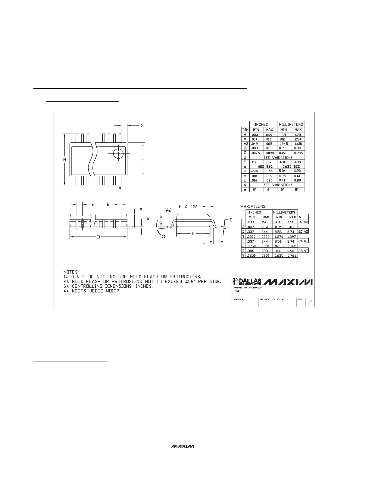
Package Information
(The package drawing(s) in this data sheet may not reflect the most current specifications. For the latest package outline information,
go to www.maxim-ic.com/packages
.
)
Revision History
Pages changes at Rev 1: 1, 12–20
QSOP.EPS
PACKAGE OUTLINE, QSOP .150", .025" LEAD PITCH
21-0055
1
F
1
 Loading...