

Page 1
General Description
The MAX8526/MAX8527/MAX8528 low-dropout linear
regulators operate from input voltages as low as 1.425V
and are able to deliver up to 2A of continuous output
current with a maximum dropout voltage of only 200mV.
The output voltage can be set from 0.5V to (VIN- 0.2V)
and is 1.4% accurate over load and line variations, from
0°C to +85°C.
These regulators use small, 2.2µF ceramic input capacitors and 10µF ceramic output capacitors to deliver 2A
output current. High bandwidth provides excellent transient response and limits the output voltage deviation to
45mV for a 20mA to 2A load step, with only a 10µF
ceramic output capacitor, and the voltage deviations can
be reduced further by increasing the output capacitor.
Designed with an internal P-channel MOSFET pass
transistor, the MAX8526/MAX8527/MAX8528 feature
low 500µA typical supply current during dropout conditions. Soft-start reduces inrush current. Other features
include a logic-controlled shutdown mode, short-circuit
protection, and thermal-overload protection.
The MAX8527 features a power-OK (POK) output that
transitions high when the regulator output is within
±10% of its nominal output voltage. The MAX8528 features a 150ms power-on reset (POR) output.
The parts are packaged in a 14-pin TSSOP package,
which includes an exposed pad for optimal power
dissipation.
Applications
Servers
Networking
Storage
Base Stations
Optical Modules
Post Regulators
Notebooks
PDAs
ATE
Features
♦ 1.425V to 3.6V Input Voltage Range
♦ Guaranteed 200mV Dropout at 2A Output Current
♦ ±0.6% Initial Accuracy
♦ ±1.4% Output Accuracy over
Load/Line/Temperature (0°C to +85°C)
♦ Compatible with Ceramic Capacitors
♦ Fast Transient Response
♦ 440µA Operating Supply Current
♦ <50µA Shutdown Supply Current
♦ Short-Circuit Protection
♦ Thermal-Overload Protection
♦ Soft-Start Limits Inrush Current
♦ 5mm x 6.4mm Footprint, 1.1mm Profile
MAX8526/MAX8527/MAX8528
1.425V to 3.6V Input, 2A,
0.2V Dropout LDO Regulators
________________________________________________________________ Maxim Integrated Products 1
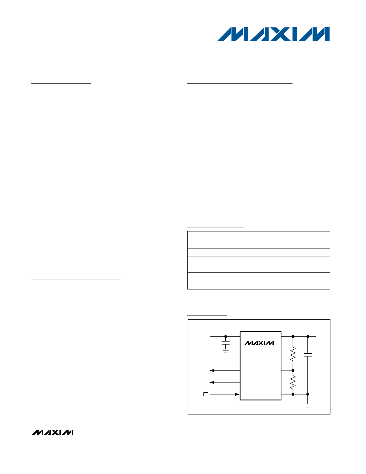
MAX8526
MAX8527
MAX8528
2.2μF
10μF
INPUT
1.425V TO 3.6V
OUTPUT
0.5V TO (V
IN
- 0.2V), 2A
POWER-ON RESET
POWER-OK
ON
OFF
IN_
POR (MAX8528)
POK (MAX8527)
EN GND
FB
OUT_
Typical Operating Circuit
Ordering Information
19-3190; Rev 1; 5/05
For pricing, delivery, and ordering information, please contact Maxim/Dallas Direct! at
1-888-629-4642, or visit Maxim’s website at www.maxim-ic.com.
Pin Configurations appear at end of data sheet.
+Denotes lead-free packaging.
PART TEMP RANGE PIN-PACKAGE
MAX8526EUD -40°C to +85°C 14 TSSOP
MAX8526EUD+ -40°C to +85°C 14 TSSOP
MAX8527EUD -40°C to +85°C 14 TSSOP
MAX8527EUD+ -40°C to +85°C 14 TSSOP
MAX8528EUD -40°C to +85°C 14 TSSOP
MAX8528EUD+ -40°C to +85°C 14 TSSOP
Page 2
MAX8526/MAX8527/MAX8528
1.425V to 3.6V Input, 2A,
0.2V Dropout LDO Regulators
2 _______________________________________________________________________________________
ABSOLUTE MAXIMUM RATINGS
ELECTRICAL CHARACTERISTICS
(Circuit of Figure 1: VIN= +1.8V, V
OUT
= +1.5V, EN = IN, I
OUT
= 2mA, TA = -40°C to +85°C, unless otherwise noted.) (Note 1)
Stresses beyond those listed under “Absolute Maximum Ratings” may cause permanent damage to the device. These are stress ratings only, and functional
operation of the device at these or any other conditions beyond those indicated in the operational sections of the specifications is not implied. Exposure to
absolute maximum rating conditions for extended periods may affect device reliability.
IN, EN, POK (MAX8527), POR (MAX8528),
FB to GND ........................................................-0.3V to +4.0V
OUT to GND ..................................................-0.3V to (IN + 0.3V)
Output Short-Circuit Duration.....................................Continuous
Continuous Power Dissipation (T
A
= +70°C,
EP soldered to PC board ground)
14-Pin TSSOP (derate 20.8mW/°C above +70°C)..............1.7W
Operating Temperature Range ...........................-40°C to +85°C
Junction Temperature......................................................+150°C
Storage Temperature Range .............................-65°C to +150°C
Lead Temperature (soldering, 10s) .................................+300°C
PARAMETER CONDITIONS
UNITS
IN
Input Voltage Range
V
Input Undervoltage Lockout VIN rising, 70mV hysteresis
V
OUT
Output Voltage Range 0.5 3.4 V
Load Regulation I
OUT
= 2mA to 2A
%/A
Line Regulation VIN = 1.425V to 3.6V, V
OUT
= 1.225V, I
OUT
= 2mA
0
% / V
Dropout Voltage (VIN - V
OUT
)VIN = 1.425V, I
OUT
= 2A, VFB = 480mV
mV
Current Limit VIN = 3.6V, V
OUT
= 3V, V
FB
= 480mV 3.2 4 4.8 A
Output Shutdown Leakage VIN = 3.6V, V
OUT
= 0, VEN = 0 0.5 50 µA
FB
I
OUT
= 20mA, TA = +85°C 497
FB Threshold Accuracy
V
OUT
= 1.225V to 3V, VIN = (V
OUT
+ 0.2V) to 3.6V,
I
OUT
= 2mA to 2A
493
mV
FB Input Bias Current VFB = 0.5V, VIN = 3.6V
1µA
MIN TYP MAX
1.425 3.600
1.32 1.35 1.38
0.08
-0.15
100 200
500 503
0.001
+0.15
507
Page 3
MAX8526/MAX8527/MAX8528
1.425V to 3.6V Input, 2A,
0.2V Dropout LDO Regulators
_______________________________________________________________________________________ 3
ELECTRICAL CHARACTERISTICS (continued)
(Circuit of Figure 1: VIN= +1.8V, V
OUT
= +1.5V, EN = IN, I
OUT
= 2mA, TA = -40°C to +85°C, unless otherwise noted.) (Note 1)
Note 1: Specifications to -40°C are guaranteed by design, not production tested.
Note 2: Measurements at high current are pulse tested, such that the junction temperature is ambient temperature. Minimum supply
voltage for output accuracy must be at least 1.425V.
PARAMETER CONDITIONS
MIN
TYP
MAX
UNITS
GND
VIN = 3.6V, V
OUT
= 3V, I
OUT
= 20mA
GND Supply Current
Dropout, V
IN
= 3.6V, VFB = 480mV
µA
GND Shutdown Current VIN = 3.6V, EN = GND 0.5 50 µA
POK (MAX8527 only)
FB high
Power-OK Threshold
V
FB
moving out of regulation,
V
HYS
= 10mV, IN = 1.425V to 3.6V
FB low
mV
POK Output Voltage Low V
FB
= 0.4V or 0.6V, I
POK
= 2mA 25
mV
POK Output Current High V
POK
= 3.6V
1µA
POK Fault Delay Time From FB to POK 25 50
µs
POR (MAX8528 only)
Power-On Reset Threshold VFB falling, V
HYS
= 10mV, VIN = 1.425V to 3.6V
mV
POR Output Voltage Low V
FB
= 0.4V or 0.6V, I
POR
= 2mA 25
mV
POR Output Current High V
POR
= 3.6V
1µA
POR Rising Delay Time From FB to POR
ms
EN
EN rising 1.2
Enable Input Threshold VIN = 1.425V to 3.6V
EN falling 0.4
V
Enable Input Bias Current VEN = 0 or 3.6V -1 +1 µA
THERMAL SHUTDOWN
TJ rising
Thermal-Shutdown Threshold Output on or off
T
J
falling
°C
OUTPUT TRANSIENT
Load Transient I
OUT
= 20mA to 2A to 20mA, t
RISE
= t
FALL
= 1µs 3 %
Line Transient δV
IN
= 0.5V, t
RISE
= t
FALL
= 5µs 3 %
440
500 800
540 550 560
440 450 460
200
0.001
100
440 450 460
200
0.001
105 150 210
+165
+150
Page 4
MAX8526/MAX8527/MAX8528
1.425V to 3.6V Input, 2A,
0.2V Dropout LDO Regulators
4 _______________________________________________________________________________________
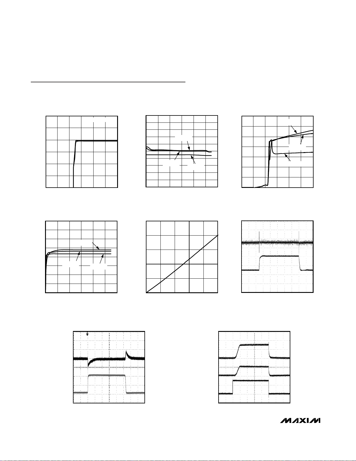
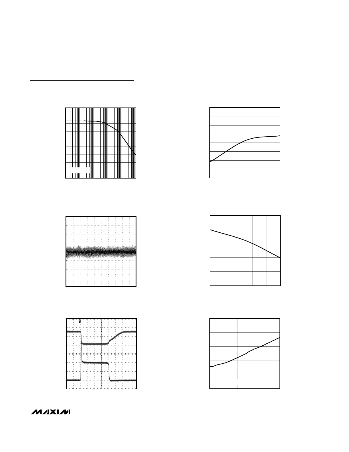
Typical Operating Characteristics
(Typical values are: V
IN
= +1.8V, V
OUT
= +1.5V, I
OUT
= 2A, C
OUT
=10µF, CIN= 2.2µF, and TA= +25°C, unless otherwise noted.)
1.30
1.40
1.35
1.50
1.45
1.55
1.60
OUTPUT VOLTAGE
vs. INPUT VOLTAGE
MAX8526/27/28 toc01
INPUT VOLTAGE (V)
OUTPUT VOTAGE (V)
0 1.2 1.80.6 2.4 3.0 3.6
TA = -40°C TO +85°C
1.490
1.493
1.492
1.491
1.494
1.495
1.496
1.497
1.498
1.499
1.500
0 800400 1200 1600 2000 2400
OUTPUT VOLTAGE
vs. LOAD CURRENT
MAX8526/27/28 toc02
LOAD CURRENT (mA)
OUTPUT VOLTAGE (V)
TA = -40°C
TA = +25°C
TA = +85°C
0
300
200
100
500
400
600
700
GROUND CURRENT
vs. INPUT VOLTAGE
MAX8526/27/28 toc03
INPUT VOLTAGE (V)
GROUND CURRENT (μA)
0 1.2 1.80.6 2.4 3.0 3.6
I
LOAD
= 2A
I
LOAD
= 0A
I
LOAD
= 1A
250
300
350
400
450
500
550
600
650
0 800400 1200 1600 2000 2400
GROUND CURRENT
vs. LOAD CURRENT
MAX8526/27/28 toc04
LOAD CURRENT (mA)
GROUND CURRENT (μA)
TA = -40°C
TA = +25°C
TA = +85°C
0
25
75
50
100
125
0 800400 1200 1600 2000
DROPOUT VOLTAGE
vs. LOAD CURRENT
MAX8526/27/28 toc05
LOAD CURRENT (mA)
DROPOUT VOLTAGE (mV)
LINE-TRANSIENT RESPONSE
(V
IN
= 1.8V TO 2.5V, I
OUT
= 2A)
MAX8526/27/28 toc06
V
OUT
10mV/div
AC-COUPLED
V
IN
500mV/div
AC-COUPLED
100μs/div
LOAD-TRANSIENT RESPONSE
(I
LOAD
= 0.2A TO 2.2A; CIN = 220μF
ELECTROLYTIC CAP CLOSE TO IN)
MAX8526/27/28 toc07
V
OUT
50mV/div
AC-COUPLED
I
LOAD
1A/div
40μs/div
2.2A
0.2A
SHUTDOWN RESPONSE
MAX8526/27/28 toc08
V
OUT
1V/div
I
IN
2A/div
EN
2V/div
100μs/div
Page 5
-10
10
0
50
40
30
20
70
60
80
0.01 10.1 10 100 1000
PSRR vs. FREQUENCY (MAX8526)
MAX8526/27/28 toc09
FREQUENCY (kHz)
PSRR (dB)
I
LOAD
= 100mA
MAX8526/MAX8527/MAX8528
1.425V to 3.6V Input, 2A,
0.2V Dropout LDO Regulators
_______________________________________________________________________________________ 5
494
496
495
500
499
498
497
501
502
-40 10-15 35 60 85
FB VOLTAGE vs. TEMPERATURE
MAX8526/27/28 toc10
TEMPERATURE (°C)
FB VOLTAGE (mV)
I
LOAD
= 20mA
OUTPUT RIPPLE VOLTAGE
MAX8526/27/28 toc11
V
OUT
1mV/div
AC-COUPLED
10μs/div
3.5
3.6
3.7
3.8
3.9
4.0
-40 10-15 35 60 85
OVERCURRENT THRESHOLD
vs. TEMPERATURE
MAX8526/27/28 toc12
TEMPERATURE (°C)
OVERCURRENT THRESHOLD (A)
SHORT-CIRCUIT CURRENT
MAX8526/27/28 TOC13
V
OUT
1V/div
I
OUT
2A/div
40μs/div
0
15
45
30
60
75
0800400 1200 1600 2000
CASE TEMPERATURE
vs. LOAD CURRENT
MAX8526/27/28 toc14
LOAD CURRENT (mA)
CASE TEMPERATURE (°C)
VIN = 2.5V; TA = +25°C
Typical Operating Characteristics (continued)
(Typical values are: V
IN
= +1.8V, V
OUT
= +1.5V, I
OUT
= 2A, C
OUT
=10µF, CIN= 2.2µF, and TA= +25°C, unless otherwise noted.)
Page 6
MAX8526/MAX8527/MAX8528
1.425V to 3.6V Input, 2A,
0.2V Dropout LDO Regulators
6 _______________________________________________________________________________________
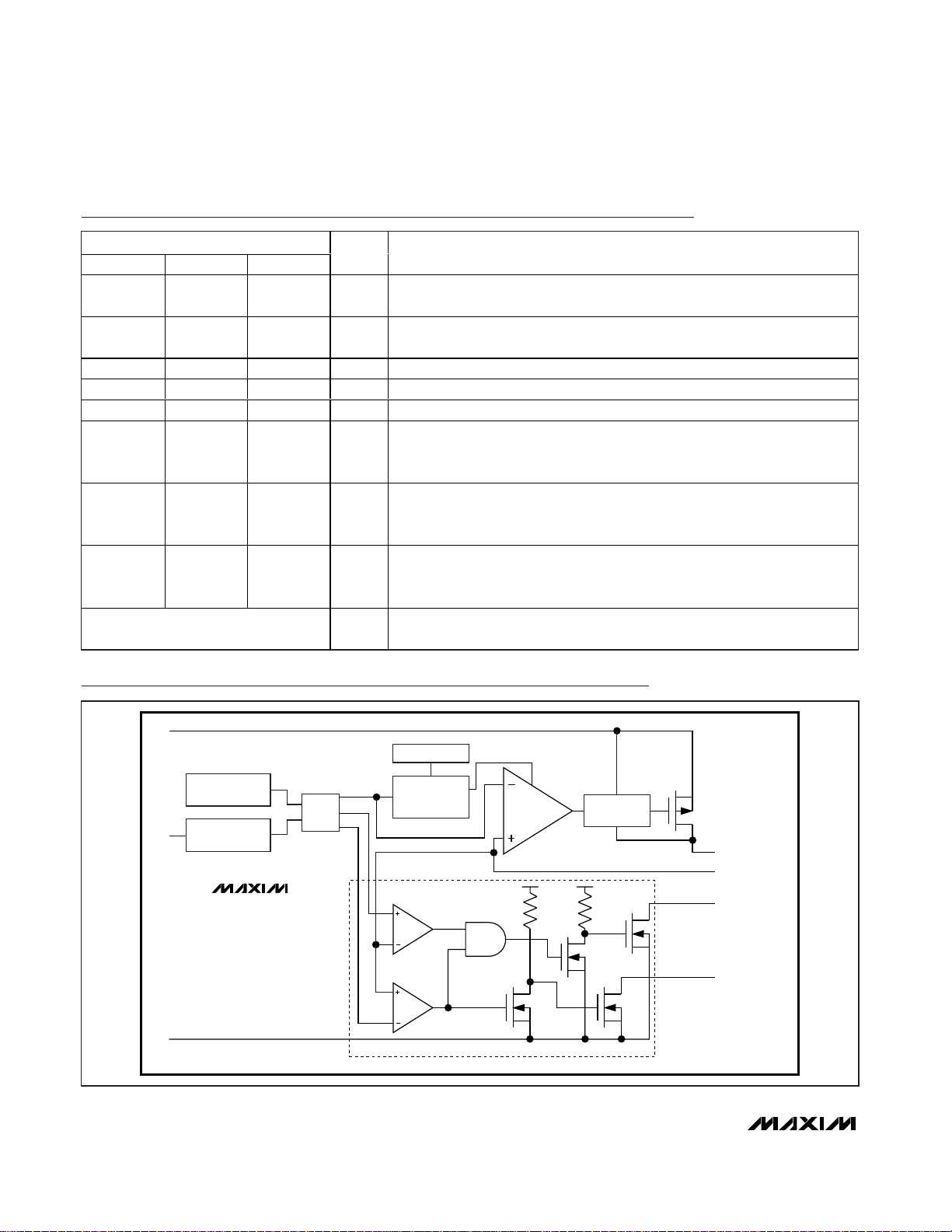
Pin Description
Functional Diagram
PIN
MAX8526
DESCRIPTION
111EN
Enable Input. Set low to place the device in low-current shutdown mode. Set
high for normal operation.
2–5 2–5 2–5 IN
Regulator Input. V
IN
can range from 1.425V to 3.6V. Bypass with a 2.2µF or
higher ceramic capacitor to GND.
6, 7, 14 7, 14 6, 14 T.P. Test Pin
888
Ground
9 9 9 FB Feedback Pin. Connect to output through a voltage-divider to set the output.
10–13 10–13 10–13
Regulator Output. Bypass with a 10µF ceramic capacitor to GND (a smaller
capacitor can be used if maximum load is less than 2A, i.e., C
OUT
= I
OUT
(max)
x (1µF/200mA).
—6—
Power-OK Output (MAX8527 Only). Open-drain output. Connect to a positive
supply with a pullup resistor. If not used, leave pin unconnected. See the
Detailed Description for more details.
—— 7
Power-On Reset Output. Open-drain output. Connect to a positive supply with
a pullup resistor. If not used, leave pin unconnected. See the Detailed
Description for more details.
Exposed Pad —
Exposed Pad on the Underside of the Package. Solder to the ground plane for
proper heat dissipation.
MAX8527 MAX8528
NAME
GND
OUT
POK
POR
IN
THRESHOLD
OVERTHERMAL
PROTECTION
EN
SHUTDOWN
LOGIC
MAX8526
MAX8527
MAX8528
GND
0.50V
0.55V
REF
0.45V
UNDERVOLTAGE
LOCKOUT
ERROR AMP
WITH
SOFT-START
MOS DRIVER
WITH I
LIMIT
OUT
FB
POK
(MAX8527 ONLY)
POR
(MAX8528 ONLY)
Page 7
MAX8526/MAX8527/MAX8528
1.425V to 3.6V Input, 2A,
0.2V Dropout LDO Regulators
_______________________________________________________________________________________ 7
Detailed Description
The MAX8526/MAX8527/MAX8528 are low-input, lowdropout, PMOS regulators capable of delivering up to
2A of output current with as little as 200mV of headroom from input to output. The PMOS output stage can
be driven from input voltages down to +1.425V without
sacrificing stability or transient performance. Since this
regulator has a PMOS output device, supply current is
not a significant function of load or input headroom.
Internal P-Channel Pass Transistor
The MAX8526/MAX8527/MAX8528 feature a 50mΩ
(typ) P-channel MOSFET pass transistor. Unlike similar
designs using PNP pass transistors, P-channel MOSFETs
require no base drive, which reduces quiescent current.
PNP-based regulators also waste considerable current in
dropout when the pass transistor saturates, and use high
base-drive currents under large loads. The MAX8526/
MAX8527/MAX8528 do not suffer from these problems
and consume only 500µA (typ) of quiescent current
under heavy loads, as well as in dropout.
Short-Circuit/Thermal Fault Protection
The MAX8526/MAX8527/MAX8528 are fully protected
from a short circuit at the output through current-limiting and thermal-overload circuitry. In the fault condition
when the output is shorted to ground, the output current is limited to 4A. Under these conditions, the part
quickly heats up. When the junction temperature reaches +165°C, the thermal-overload circuitry turns off the
output, allowing the part to cool down. When the junction temperature cools to +150°C, the output turns
back on and tries to reestablish regulation. Current
limiting and thermal protection continue until the fault is
removed. For continuous operation, do not exceed the
absolute maximum junction temperature rating of
TJ= +150°C.
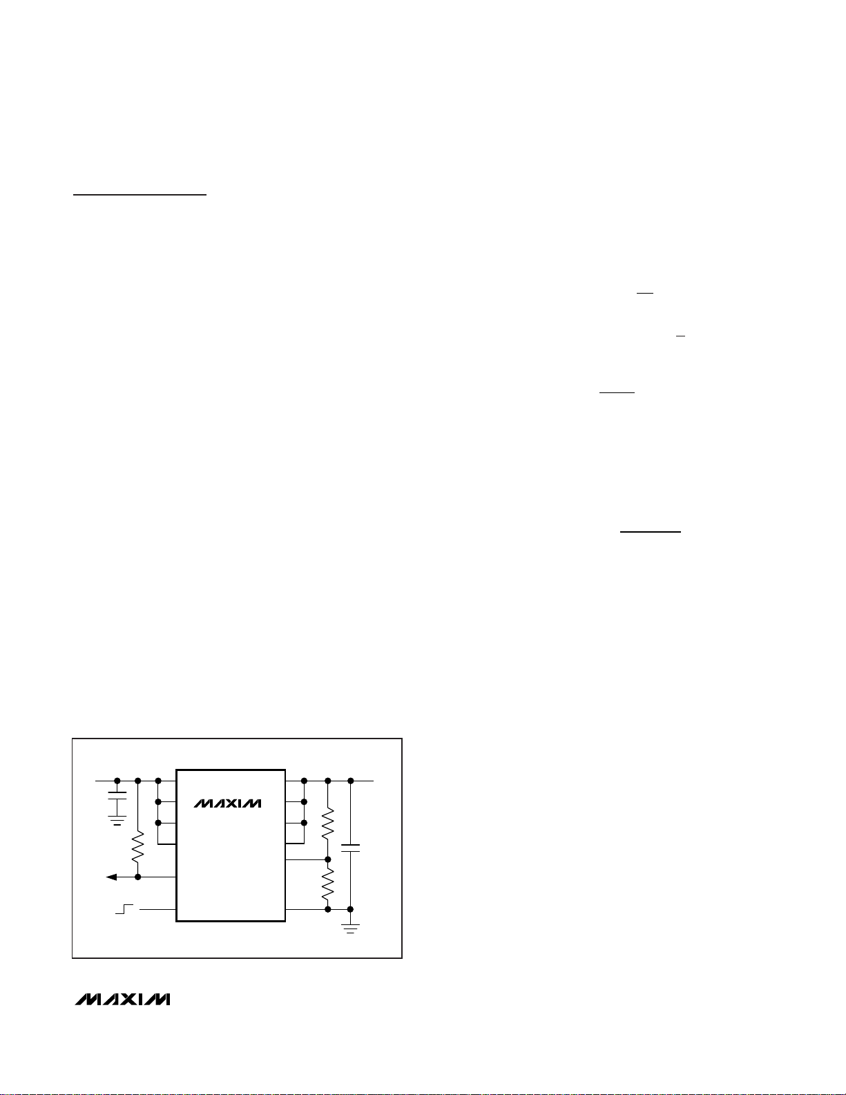
Output Voltage Selection
The MAX8526/MAX8527/MAX8528 feature an
adjustable output voltage from 0.5V to 3.4V, using two
external resistors connected as a voltage-divider to FB
as shown in Figure 1. The output voltage is set by the
following equation:
where typically V
FB
= 0.5V. Choose R2 < 5kΩ to opti-
mize quiescent current, accuracy, and high-frequency
power-supply rejection. To simplify resistor selection:
Soft-Start
Inherent soft-start limits inrush current. Peak inrush current is dependent on the value of C
OUT
and can be
calculated as follows:
Shutdown Mode
The MAX8526/MAX8527/MAX8528 include an enable
input. To shut down the device, pull EN to GND. For
normal operation, connect the EN to IN. During shutdown, an internal 10kΩ resistor pulls down the output.
Power-OK (POK, MAX8527 Only)
The MAX8527 features a power-OK output to indicate
the status of the output. POK remains high when the
regulator output is within ±10% of its nominal output
voltage. If the output voltage falls/rises outside this
range, POK transitions low. This open-drain output
requires an external pullup resistor to IN. An internal
delay circuit prevents the POK from switching for 50µs
(typ) after the trip threshold is initially reached. If the
part is in shutdown mode, POK is low.
Power-On Reset (POR, MAX8528 Only)
The MAX8528 features a power-on reset output that
transitions high 150ms (typ) after the output has risen
above 90% of its final value. This open-drain output
requires an external pullup resistor to IN. If the part is in
shutdown mode, falls below 90% of the nominal output
voltage, or experiences a short-circuit/thermal fault,
POR immediately transitions low.
II
CF
INRUSH LOAD
OUT
=+
()
⎛
⎝
⎜
⎞
⎠
⎟
μ
66
RR
V
V
OUT
FB
12 =
⎛
⎝
⎜
⎞
⎠
⎟
-1
VV
R
R
OUT FB
=+
⎛
⎝
⎜
⎞
⎠
⎟
1
1
2
MAX8526
MAX8527
MAX8528
2.2μF
10μF
ENABLE
SHUTDOWN
IN
IN
POK (MAX8527) OR
POR (MAX8528)
EN
IN
IN
OUT
OUT
GND
FB
OUT
OUT
100kΩ*
R1
R2
ADJUSTABLE
OUTPUT
*FOR MAX8527 AND MAX8528
+1.425V TO +3.6V
Figure 1. Typical Application Circuit
Page 8

Chip Information
TRANSISTOR COUNT: 2977
PROCESS: BiCMOS
MAX8526/MAX8527/MAX8528
Operating Region and Power Dissipation
The maximum power dissipation depends on the thermal resistance of the IC package and circuit board, the
temperature difference between the die junction and
ambient air, and the rate of airflow. The power dissipated in the device is P = I
OUT
x (VIN- V
OUT
).
The package features an exposed thermal pad on its
underside. This pad lowers the thermal resistance of
the package by providing a direct heat conduction
path from the die to the PC board.
Additionally, the ground pins (GND) perform the dual
function of providing an electrical connection to system
ground and channeling heat away. Connect the
exposed backside pad and GND to the system ground
using a large pad or ground plane, or multiple vias to
the ground-plane layer.
Applications Information
Capacitor Selection and
Regulator Stability
Capacitors are required at the MAX8526/MAX8527/
MAX8528 inputs and outputs for stable operation over
the full temperature range and with load currents up to
2A. Connect a 2.2µF capacitor between IN and ground
and a 10µF capacitor with low equivalent-series-resistance (ESR) capacitor between OUT and ground for 2A
output current. The input capacitor (C
IN
) lowers the
source impedance of the input supply. If input-supply
source impedance is high, place a larger input capacitor close to IN to prevent VINsagging due to load transients. Smaller output capacitors can be used for output
currents less than 2A. Calculate C
OUT
as follows:
C
OUT
= I
OUT(max)
✕ (1µF / 200mA)
Noise, PSRR, and Transient Response
The MAX8526/MAX8527/MAX8528 are designed to
operate with low dropout voltages and low quiescent
currents, while still maintaining good noise, transient
response, and AC rejection. See the Typical Operating
Characteristics for a plot of Power-Supply Rejection
Ratio (PSRR) vs. Frequency. When operating from
noisy sources, improved supply-noise rejection and
transient response can be achieved by increasing the
values of the input and output bypass capacitors and
through passive filtering techniques. The MAX8526/
MAX8527/MAX8528 load-transient response graphs
(see the Typical Operating Characteristics) show two
components of the output response: a DC shift from the
output impedance due to the load current change, and
the transient response. A typical transient overshoot for
a step change in the load current from 20mA to 2A is
45mV. Use larger output ceramic capacitors greater
than 10µF up to 100µF to attenuate the overshoot.
1.425V to 3.6V Input, 2A,
0.2V Dropout LDO Regulators
8 _______________________________________________________________________________________
TOP VIEW
14
13
12
11
10
9
8
1
2
3
4
5
6
7
T.P.
OUT
OUT
OUTIN
IN
IN
EN
MAX8526
OUT
FB
GNDT.P.
T.P.
IN
TSSOP
14
13
12
11
10
9
8
1
2
3
4
5
6
7
T.P.
OUT
OUT
OUTIN
IN
IN
EN
MAX8527
OUT
FB
GNDT.P.
POK
IN
TSSOP
14
13
12
11
10
9
8
1
2
3
4
5
6
7
T.P.
OUT
OUT
OUTIN
IN
IN
EN
MAX8528
OUT
FB
GNDPOR
T.P.
IN
TSSOP
Pin Configurations
Page 9

MAX8526/MAX8527/MAX8528
1.425V to 3.6V Input, 2A,
0.2V Dropout LDO Regulators
Maxim cannot assume responsibility for use of any circuitry other than circuitry entirely embodied in a Maxim product. No circuit patent licenses are
implied. Maxim reserves the right to change the circuitry and specifications without notice at any time.
Maxim Integrated Products, 120 San Gabriel Drive, Sunnyvale, CA 94086 408-737-7600 _____________________ 9
© 2005 Maxim Integrated Products Printed USA is a registered trademark of Maxim Integrated Products, Inc.
Package Information
(The package drawing(s) in this data sheet may not reflect the most current specifications. For the latest package outline information
go to www.maxim-ic.com/packages
.)
AA AA
TSSOP 4.4mm BODY.EPS
 Loading...