

Page 1
General Description
The MAX8520/MAX8521 are designed to drive thermoelectric coolers (TECs) in space-constrained optical
modules. Both devices deliver ±1.5A output current
and control the TEC current to eliminate harmful current
surges. On-chip FETs minimize external components and
high switching frequency reduces the size of external
components.
The MAX8520 and MAX8521 operate from a single supply
and bias the TEC between the outputs of two synchronous buck regulators. This operation allows for temperature control without “dead zones” or other nonlinearities
at low current. This arrangement ensures that the control
system does not hunt when the set point is very close to
the natural operating point, requiring a small amount of
heating or cooling. An analog control signal precisely
sets the TEC current.
Both devices feature accurate, individually adjustable
heating current limit and cooling current limit, along
with maximum TEC voltage limit to improve the reliability
of optical modules. An analog output signal monitors
the TEC current. A unique ripple cancellation scheme
helps reduce noise.
The MAX8520 is available in a 5mm x 5mm thin QFN
package and its switching frequency is adjustable up to
1MHz through an external resistor. The MAX8521 is also
available in a 5mm x 5mm thin QFN, as well as a spacesaving 3mm x 3mm UCSP™, with a pin-selectable
switching frequency of 500kHz or 1MHz.
Applications
SFF/SFP Modules
Fiber-Optic Laser Modules
Fiber-Optic Network Equipment
ATE
Biotech Lab Equipment
Features
♦ Circuit Footprint of 0.31in
2
♦ Low-Profile Design
♦ On-Chip Power MOSFETs
♦ High-Efficiency Switch-Mode Design
♦ Ripple Cancellation for Low Noise
♦ Direct Current Control Prevents TEC Current
Surges
♦ 5% Accurate Adjustable Heating/Cooling Current
Limits
♦ 2% Accurate TEC Voltage Limit
♦ No Dead Zone or Hunting at Low Output Current
♦ ITEC Monitors TEC Current
♦ 1% Accurate Voltage Reference
♦ Switching Frequency Up to 1MHz
♦ Synchronization (MAX8521)
MAX8520/MAX8521
Smallest TEC Power Drivers for
Optical Modules
________________________________________________________________ Maxim Integrated Products 1
Ordering Information
19-2586; Rev 0; 10/02
For pricing, delivery, and ordering information, please contact Maxim/Dallas Direct! at
1-888-629-4642, or visit Maxim’s website at www.maxim-ic.com.
EVALUATION KIT
AVAILABLE
PART TEMP RANGE PIN-PACKAGE
MAX8520ETP
20 Thin QFN 5mm x 5mm
MAX8521EBX
36 UCSP 3mm x 3mm
MAX8521ETP
20 Thin QFN 5mm x 5mm
UCSP is a trademark of Maxim Integrated Products, Inc.
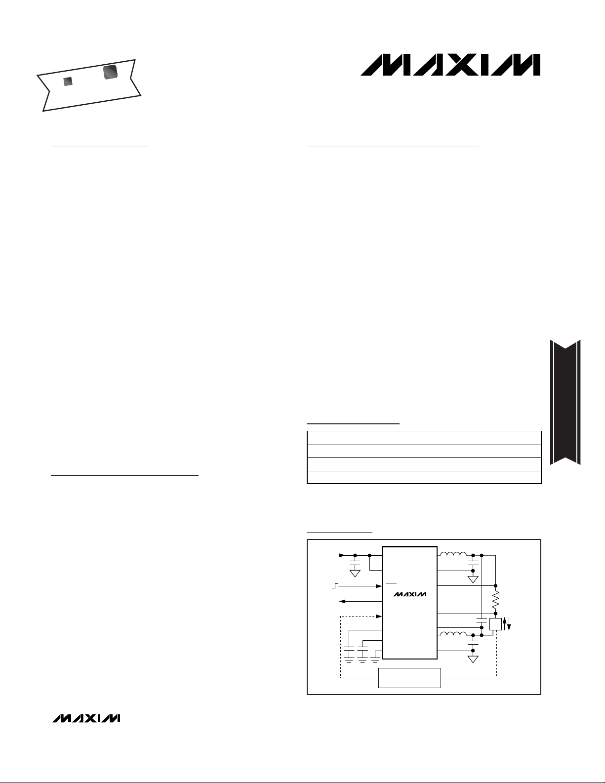
INPUT
3V TO 5.5V
V
DD
PV
DD
COMP
GND
SHDN
ITEC
ON
OFF
TEC CURRENT
MONITOR
CTLI
LX1
PGND1
CS
OS1
OS2
LX2
PGND2
TEC
I
TEC
= ± 1.5A
REF
CURRENT-
CONTROL
SIGNAL
FREQ
ANALOG /DIGITAL
TEMPERATURE CONTROL
OUTPUT
MAX8521
Typical Operating Circuit
Pin Configurations appear at end of data sheet.
3mm x 3mm
CSP
5mm x 5mm
QFN
-40°C to +85°C
-40°C to +85°C
-40°C to +85°C
Page 2
MAX8520/MAX8521
Smallest TEC Power Drivers for
Optical Modules
2 _______________________________________________________________________________________
ABSOLUTE MAXIMUM RATINGS
Stresses beyond those listed under “Absolute Maximum Ratings” may cause permanent damage to the device. These are stress ratings only, and functional
operation of the device at these or any other conditions beyond those indicated in the operational sections of the specifications is not implied. Exposure to
absolute maximum rating conditions for extended periods may affect device reliability.
VDDto GND..............................................................-0.3V to +6V
SHDN, MAXV, MAXIP, MAXIN,
CTLI to GND .........................................................-0.3V to +6V
COMP, FREQ, OS1, OS2, CS, REF,
ITEC to GND...........................................-0.3V to (V
DD
+ 0.3V)
PV
DD
1, PVDD2 to GND...............................-0.3V to (VDD+ 0.3V)
PV
DD
1, PVDD2 to VDD...........................................-0.3V to +0.3V
PGND1, PGND2 to GND .......................................-0.3V to +0.3V
COMP, REF, ITEC Short to GND ...................................Indefinite
LX Current (Note 1) ........................................±2.25A LX Current
Continuous Power Dissipation (T
A
= +70°C)
20-Pin 5mm x 5mm x 0.9mm QFN (derate 20.8mW/°C
above +70°C) (Note 2)...................................................1.67W
3mm x 3mm UCSP (derate 22mW/°C
above +70°C).................................................................1.75W
Maximum Junction Temperature .....................................+150°C
Storage Temperature Range .............................-65°C to +150°C
Lead Temperature (soldering 10s) ..................................+300°C
ELECTRICAL CHARACTERISTICS
(VDD= PVDD1 = PVDD2 = SHDN = 5V, 1MHz mode (Note 3). PGND1 = PGND2 = GND, CTLI = MAXV = MAXIP = MAXIN = REF,
T
A
= 0°C to +85°C, unless otherwise noted. Typical values at TA= +25°C.)
PARAMETER
SYMBOL
CONDITIONS
MIN
TYP
MAX
UNITS
Input Supply Range V
DD
3.0 5.5 V
Maximum TEC Current
A
Reference Voltage V
REF
V
DD
= 3V to 5.5V, I
REF
= 150µA
1.5
V
Reference Load Regulation ∆V
REF
V
DD
= 3V to 5V, I
REF
= 10µA to 1mA 1.2 5.0 mV
V
MAXI_
= V
REF
160
V
DD
= 5V
V
MAXI_
= V
REF
/3 40 50 60
V
MAXI_
= V
REF
155
MAXIP/MAXIN Threshold
Accuracy
V
DD
= 3V
V
MAXI_
= V
REF
/3 45 50 55
mV
V
DD
= 5V, I = 0.2A
NFET On-Resistance
)
V
DD
= 3V, I = 0.2A
Ω
V
DD
= 5V, I = 0.2A
PFET On-Resistance
)
V
DD
= 3V, I = 0.2A
Ω
VLX = V
DD
= 5V, TA = +25°C
4
NFET Leakage I
LEAK(N)
VLX = V
DD
= 5V, TA = +85°C 0.3
µA
VLX = 0, TA = +25°C
4
PFET Leakage I
LEAK(P)
VLX = 0, TA = +85°C 0.3
µA
500kHz mode 11 14
V
COMP
= V
REF
=
1.500V, V
DD
= 5V
1MHz mode 16 21
500kHz mode 8 11
No-Load Supply Current
I
DD(NO
LOAD)
V
COMP
= V
REF
=
1MHz mode 11 14
mA
Shutdown Supply Current I
DD-SD
SHDN = GND, V
DD
= 5V (Note 4) 2 3 mA
Thermal Shutdown
Hysteresis = 15°C
°C
VDD rising
UVLO Threshold V
UVLO
VDD falling
V
Note 1: LX has internal clamp diodes to PGND and PVDD. Applications that forward bias these diodes should take care not to exceed
the IC’s package power dissipation limits.
Note 2: Solder underside metal slug to PC board ground plane.
R
DS(ON-N
R
DS(ON-P
T
SHUTDOWN
1.500V, V
DD
= 3.3V
±1.5
1.485
1.515
140 150
143 150
0.09 0.14
0.11 0.16
0.14 0.23
0.17 0.30
0.03
0.03
+165
2.50 2.65 2.80
2.40 2.55 2.70
Page 3
MAX8520/MAX8521
Smallest TEC Power Drivers for
Optical Modules
_______________________________________________________________________________________ 3
ELECTRICAL CHARACTERISTICS (continued)
(VDD= PVDD1 = PVDD2 = SHDN = 5V, 1MHz mode (Note 3). PGND1 = PGND2 = GND, CTLI = MAXV = MAXIP = MAXIN = REF,
T
A
= 0°C to +85°C, unless otherwise noted. Typical values at TA= +25°C.)
PARAMETER
SYMBOL
CONDITIONS
MIN
TYP
MAX
UNITS
MAX8521, FREQ= VDD, V
DD
= 3V to 5V 0.8 1 1.2
MAX8521, FREQ= 0, V
DD
= 3V to 5V 0.4 0.5 0.6
MAX8520, R
EXT
= 60kΩ, V
DD
= 5V 0.8 1 1.2
MAX8520, R
EXT
= 60kΩ, V
DD
= 3V
MAX8520, R
EXT
= 150kΩ, V
DD
= 5V 0.4 0.5 0.6
Internal Oscillator Switching
Frequency
f
SW-INT
MAX8520, R
EXT
= 150kΩ, V
DD
= 3V
MHz
External Sync Frequency Range
25% < duty cycle <75% (MAX8521 only) 0.7 1.2
MHz
LX_ Duty Cycle (Note 5) 0 100 %
OS1, OS2, CS Input Current
I
OS1
, I
OS2
,
I
CS
0 or V
DD
µA
SHDN, FREQ Input Current
I
SHDN
,
I
FREQ
0 or VDD, FREQ applicable for the
MAX8521 only
-5 +5 µA
SHDN, FREQ Input Low Voltage V
IL
V
DD
= 3V to 5.5V, FREQ applicable for the
MAX8521 only
V
SHDN, FREQ Input High Voltage
V
IH
V
DD
= 3V to 5.5V, FREQ applicable for the
MAX8521 only
VDD x
V
V
MAXV
= V
REF
x 0.67, V
OS1
to V
OS2
= ±4V,
V
DD
= 5V
-2 +2 %
MAXV Threshold Accuracy
V
MAXV
= V
REF
x 0.33, V
OS1
to V
OS2
= ±2V,
V
DD
= 3V
-3 +3 %
MAXV, MAXI_ Input Bias Current
I
MAXV-BIAS
,
V
MAXV
= V
MAXI_
= 0.1V or 1.5V
µA
CTLI Gain A
CTLI
V
CTLI
= 0.5V to 2.5V (Note 6) 9.5 10
V/V
CTLI Input Resistance R
CTLI
1MΩ terminated at REF 0.5 1 2.0 MΩ
Error-Amp Transconductance g
m
50
160 µS
V
ITEC
Accuracy V
OS1
to VCS = ±100mV, V
OS1
= VDD/2 -10
%
0.76 0.93 1.10
0.36 0.46 0.56
-100 +100
0.75
I
MAXI_-BIAS
-0.1 +0.1
100
VDD x
0.25
10.5
+10
Page 4
MAX8520/MAX8521
Smallest TEC Power Drivers for
Optical Modules
4 _______________________________________________________________________________________
ELECTRICAL CHARACTERISTICS
(VDD= PVDD1 = PVDD2 = SHDN = 5V, 1MHz mode (Note 2). PGND1 = PGND2 = GND, CTLI = MAXV = MAXIP = MAXIN = REF, TA=
-40°C to +85°C, unless otherwise noted.) (Note 7)
PARAMETER
SYMBOL
CONDITIONS
MIN
MAX
UNITS
Input Supply Range V
DD
3.0 5.5 V
Maximum TEC Current
A
Reference Voltage V
REF
V
DD
= 3V to 5.5V, I
REF
= 150µA
V
Reference Load Regulation ∆V
REF
V
DD
= 3V to 5V, I
REF
= 10µA to 1mA 5 mV
V
MAXI_
= V
REF
140 160
V
DD
= 5V
V
MAXI_
= V
REF
/3 40 60
V
MAXI_
= V
REF
143 155
MAXIP/MAXIN Threshold
Accuracy
V
DD
= 3V
V
MAXI_
= V
REF
/3 45 55
mV
V
DD
= 5V, I = 0.2A
NFET On-Resistance
)
V
DD
= 3V, I = 0.2A
Ω
V
DD
= 5V, I = 0.2A
PFET On-Resistance
)
V
DD
= 3V, I = 0.2A
Ω
500kHz mode 14
V
COMP
= V
REF
=
1.500V, V
DD
= 5V
1MHz mode 21
500kHz mode 11
No-Load Supply Current
I
DD(NO
LOAD)
V
COMP
= V
REF
=
1MHz mode 14
mA
Shutdown Supply Current I
DD-SD
SHDN = GND, V
DD
= 5V (Note 4) 3 mA
VDD rising
UVLO Threshold V
UVLO
VDD falling
V
MAX8521, FREQ = VDD, V
DD
= 3V to 5V 0.8 1.2
MAX8521, FREQ = 0, V
DD
= 3V to 5V 0.4 0.6
MAX8520, R
EXT
= 60kΩ, V
DD
= 5V 0.8 1.2
MAX8520, R
EXT
= 60kΩ, V
DD
= 3V
MAX8520, R
EXT
= 150kΩ, V
DD
= 5V 0.4 0.6
Internal Oscillator Switching
Frequency
f
SW-INT
MAX8520, R
EXT
= 150kΩ, V
DD
= 3V
MHz
25% < duty cycle <75% (MAX8521 only) 0.7 1.2
MHz
LX_ Duty Cycle (Note 5) 0 100 %
OS1, OS2, CS Input Current
I
OS1
, I
OS2
,
I
CS
0 or V
DD
µA
SHDN, FREQ Input Current
I
SHDN
,
I
FREQ
0 or VDD, FREQ applicable for the MAX8521
only
-5 +5 µA
SHDN, FREQ Input Low Voltage V
IL
V
DD
= 3V to 5.5V, FREQ applicable for the
MAX8521 only
VDD x
V
V
IH
V
DD
= 3V to 5.5V, FREQ applicable for the
MAX8521 only
VDD x
V
±1.5
1.480 1.515
R
DS(ON-N
External Sync Frequency Range
SHDN, FREQ Input High Voltage
R
DS(ON-P
1.500V, V
DD
= 3.3V
2.50 2.80
2.40 2.70
0.76 1.10
0.36 0.56
-100 +100
0.75
0.14
0.16
0.23
0.30
0.25
Page 5
MAX8520/MAX8521
Smallest TEC Power Drivers for
Optical Modules
_______________________________________________________________________________________ 5
ELECTRICAL CHARACTERISTICS (continued)
(VDD= PVDD1 = PVDD2 = SHDN = 5V, 1MHz mode (Note 2). PGND1 = PGND2 = GND, CTLI = MAXV = MAXIP = MAXIN = REF, TA=
-40°C to +85°C, unless otherwise noted.) (Note 7)
PARAMETER
CONDITIONS
UNITS
V
MAXV
= V
REF
x 0.67, V
OS1
to V
OS2
= ±4V,
V
DD
= 5V
-2 +2 %
MAXV Threshold Accuracy
V
MAXV
= V
REF
x 0.33, V
OS1
to V
OS2
= ±2V,
V
DD
= 3V
-3 +3 %
I
MAXV-
BIAS
,
V
MAXV
= V
MAXI_
= 0.1V or 1.5V
µA
CTLI Gain A
CTLI
V
CTLI
= 0.5V to 2.5V (Note 6) 9.5
V/V
CTLI Input Resistance R
CTLI
1MΩ terminated at REF 0.5 2.0 MΩ
Error-Amp Transconductance g
m
50 160 µS
V
ITEC
Accuracy V
OS1
to VCS = ±100mV, V
OS1
= VDD/2 -10
%
Note 3: Enter 1MHz mode by tying a 60kΩ resistor from FREQ to ground for the MAX8520, and tying FREQ to VDDfor the MAX8521.
Note 4: Includes PFET leakage.
Note 5: Duty-cycle specification is guaranteed by design and not production tested.
Note 6: CTLI Gain is defined as:
Note 7: Specifications to -40°C are guaranteed by design and not production tested.
A
V
VV
CTLI
CTLI
OS CS
=
−
()
∆
∆
1
Typical Operating Characteristics
(VDD= 5V, circuit of Figure 1, TA= +25°C, unless otherwise noted)
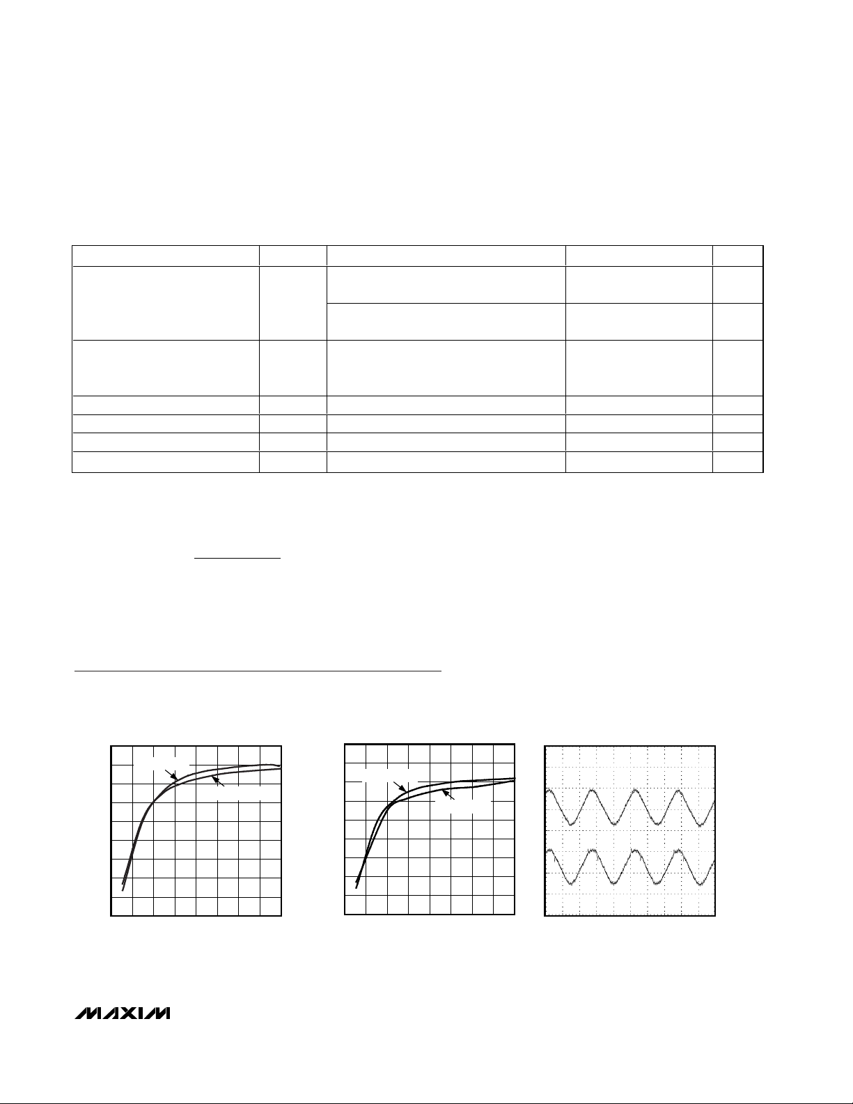
EFFICIENCY vs. TEC CURRENT
(V
DD
= 5V, R
TEC
= 2Ω)
MAX8520/21 toc01
TEC CURENT (A)
EFFICIENCY (%)
1.41.20.8 1.00.4 0.60.2
10
20
30
40
50
60
70
80
90
0
0 1.6
FREQ = 500kHz
FREQ = 1MHz
EFFICIENCY vs. TEC CURRENT
(V
DD
= 3.3V, R
TEC
= 1.3Ω)
MAX8520/21 toc02
TEC CURRENT (A)
EFFICIENCY (%)
1.41.20.8 1.00.4 0.60.2
10
20
30
40
50
60
70
80
90
0
0 1.6
FREQ = 500kHz
FREQ = 1MHz
COMMON-MODE
OUTPUT VOLTAGE RIPPLE
MAX8520/21 toc03
400ns/div
V
OS2
20mV/div
AC-COUPLED
V
OS1
20mV/div
AC-COUPLED
I
TEC
= 1A
C
2
= C7 = 1µF
MAXV, MAXI_ Input Bias Current
SYMBOL
I
MAXI_-BIAS
MIN MAX
-0.1 +0.1
10.5
+10
Page 6
MAX8520/MAX8521
Smallest TEC Power Drivers for
Optical Modules
6 _______________________________________________________________________________________
DIFFERENTIAL
OUTPUT VOLTAGE RIPPLE
MAX8520/21 toc04
400ns/div
V
OS2
- V
OS1
1mV/div
AC-COUPLED
C
2
= C7 = 1µF
I
TEC
= 1A
VDD RIPPLE
MAX8520/21 toc05
400ns/div
V
DD
20mV/div
AC-COUPLED
I
TEC
= 1A
TEC CURRENT RIPPLE
MAX8520/21 toc06
400ns/div
10mA/div
AC-COUPLED
0A
1.5A
TEC CURRENT vs. CTLI VOLTAGE
MAX8520/21 toc07
20ms/div
V
CTLI
1V/div
I
TEC
1A/div
0A
0V
ZERO-CROSSING TEC CURRENT
MAX8520/21 toc08
1ms/div
V
CTLI
I00mV/div
I
TEC
100mA/div
0A
1.5V
V
ITEC
vs. TEC CURRENT
MAX8520/21 toc09
TEC CURRENT (A)
V
ITEC
(V)
1.51.00.50-0.5-1.0-1.5
0.5
1.0
1.5
2.0
2.5
3.0
0
-2.0 2.0
Typical Operating Characteristics (continued)
(VDD= 5V, circuit of Figure 1, TA= +25°C, unless otherwise noted)
I
TEC
vs. AMBIENT TEMPERATURE
MAX8520/21 toc10
AMBIENT TEMPERATURE (°C)
TEC CURRENT (A)
6040200-20
0.460
0.470
0.480
0.490
0.500
0.510
0.520
0.450
-40 80
FREQ = 1MHz
V
CTLI
= 2V
R
TEC
= 1Ω
SWITCHING FREQUENCY
vs. TEMPERATURE
MAX8520/21 toc11
TEMPERATURE (°C)
SWITCHING FREQUENCY (kHz)
806040200-20
500
600
700
800
900
1000
1100
400
-40
FREQ = 1MHz
V
CTLI
= 1.5V
R
TEC
= 1Ω
FREQ = 500kHz
Page 7

MAX8520/MAX8521
Smallest TEC Power Drivers for
Optical Modules
_______________________________________________________________________________________ 7
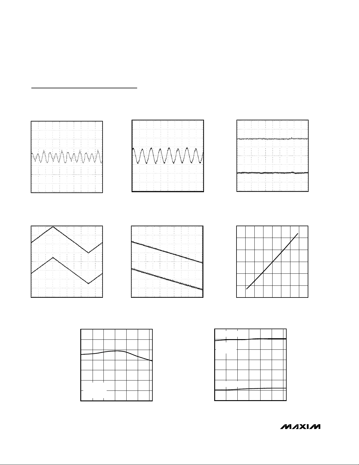
SWITCHING FREQUENCY CHANGE vs. V
DD
MAX8520/21 toc12
VDD (V)
SWITCHING FREQUENCY CHANGE (kHz)
5.04.54.03.5
200
400
600
800
1000
1200
0
3.0 5.5
FREQ = 500kHz
FREQ = 1MHz
SWITCHING FREQUENCY vs. R
EXT
MAX8520/21 toc13
R
EXT
(kΩ)
SWITCHING FREQUENCY (kHz)
14012010080
500
600
700
800
900
1000
1100
400
60 160
VDD = 3.3V
VDD = 5V
VDD STEP RESPONSE
MAX8520/21 toc19
10ms/div
V
DD
2V/div
I
TEC
10mA/div
1A
0V
REFERENCE VOLTAGE CHANGE vs. V
DD
MAX8520/21 toc14
VDD (V)
REFERENCE VOLTAGE CHANGE (mV)
5.04.54.03.5
-1.2
-1.0
-0.8
-0.6
-0.4
-0.2
0.0
0.2
0.4
0.6
-1.4
3.0 5.5
REF SOURCING 150µA
REFERENCE VOLTAGE CHANGE
vs. TEMPERATURE
MAX8520/21 toc15
TEMPERATURE (°C)
REFERENCE VOLTAGE CHANGE (mV)
8040 600 20-20
-4
-3
-2
-1
0
1
2
3
4
5
-5
-40
REF SOURCING 150µA
REFERENCE VOLTAGE CHANGE
vs. LOAD CURRENT
MAX8520/21 toc16
LOAD CURRENT (mA)
REFERENCE VOLTAGE CHANGE (mV)
0.80.60.40.2
-10
-8
-6
-4
-2
0
-12
0 1.0
STARTUP AND SHUTDOWN WAVEFORMS
MAX8520/21 toc17
200µs/div
V
SHDN
5V/div
I
TEC
500mA/div
I
DD
200mA/div
0mA
0mA
0V
CTLI STEP RESPONSE
MAX8520/21 toc18
1ms
V
CTLI
1V/div
I
TEC
1A/div
0A
1.5V
Typical Operating Characteristics (continued)
(VDD= 5V, circuit of Figure 1, TA= +25°C unless otherwise noted)
Page 8
MAX8520/MAX8521
Smallest TEC Power Drivers for
Optical Modules
8 _______________________________________________________________________________________
Typical Operating Characteristics (continued)
(VDD= 5V, circuit of Figure 1, TA= +25°C unless otherwise noted)
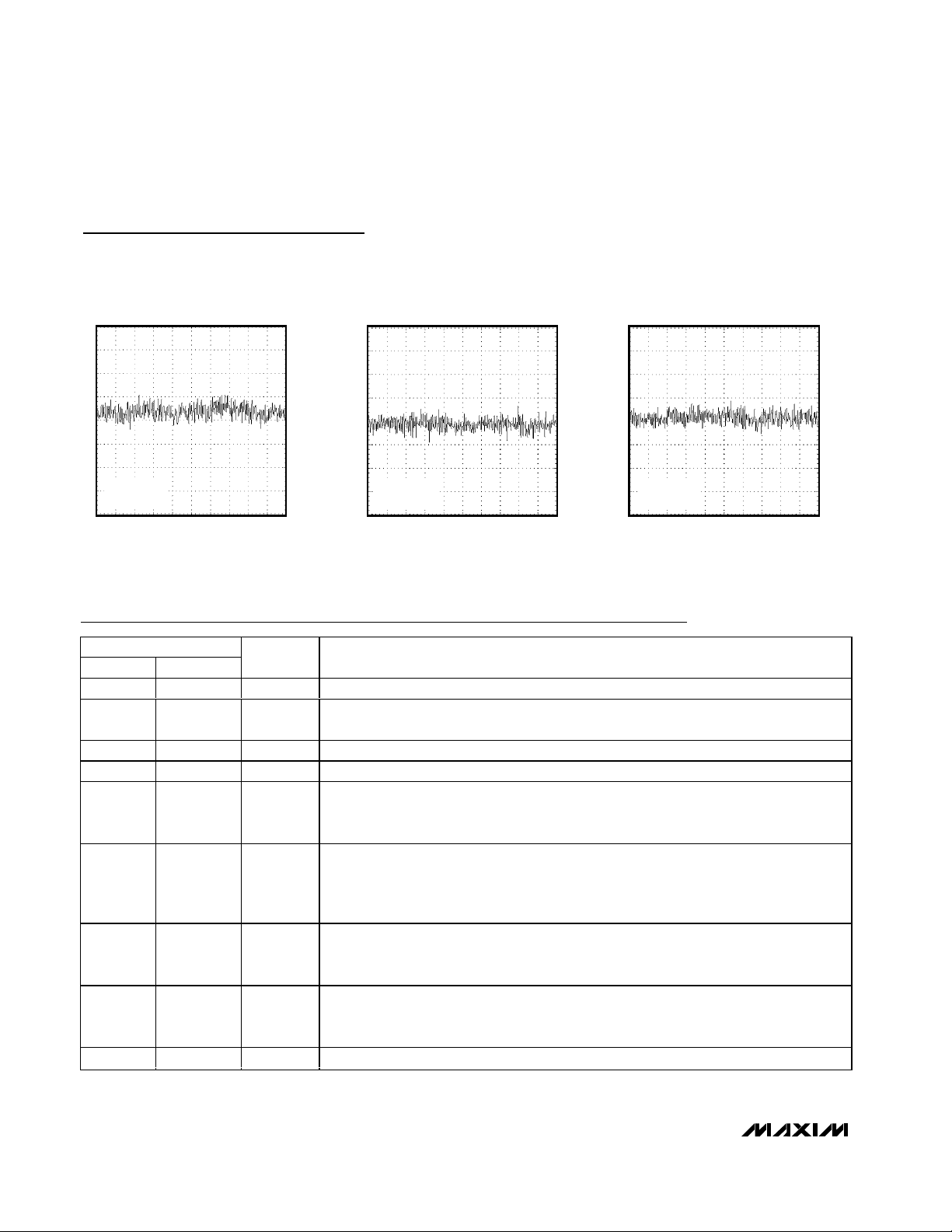
THERMAL STABILITY,
COOLING MODE
MAX8520/21 toc20
4s/div
TEMPERATURE
0.001°C/div
T
TEC
= +25°C
T
A
= +45°C
THERMAL STABILITY,
ROOM TEMPERATURE
MAX8520/21 toc21
4s/div
TEMPERATURE
0.001°C/div
T
TEC
= +25°C
T
A
= +25°C
THERMAL STABILITY,
HEATING MODE
MAX8520/21 toc22
4s/div
TEMPERATURE
0.001°C/div
T
TEC
= +25°C
T
A
= +5°C
Pin Description
PIN
QFN UCSP
NAME FUNCTION
1 E1, E2 LX1 Inductor Connection. LX1 is high-impedance in shutdown.
2
PGND1
Power Ground 1. Internal synchronous-rectifier ground connection. Connect all PGND
pins together at power ground plane.
3C1SHDN Shutdown Control Input. Pull SHDN low to turn off PWM control and ITEC output.
4 C2 COMP Current-Control Loop Compensation. Refer to the Compensation Capacitor section.
5 B1 ITEC
TEC Current-Monitor Output. The ITEC output voltage is a function of the voltage across
the TEC current-sense resistor. V
ITEC
= V
REF
+ 8 (V
OS
- VCS). Keep capacitance on ITEC
<150pF.
6 A1 MAXIN
Maximum Negative TEC Current. Connect MAXIN to REF to set default negative current
limit to -150mV/R
SENSE
. To lower this current limit, connect MAXIN to a resistor divider
network from REF to GND. The current limit will then be equal to -(V
MAXIN/VREF
) x
(150mV/R
SENSE
).
7 A2 MAXIP
Maximum Positive TEC Current. Connect MAXIP to REF to set default positive current limit
to 150mV/R
SENSE
. To lower this current limit, connect MAXIP to a resistor divider network
from REF to GND. The current limit will then be equal to (V
MAXIP/VREF
) x (150mV/R
SENSE
).
8 A3 MAXV
Maximum Bipolar TEC Voltage. Connect MAXV to REF to set default maximum TEC
voltage to VDD. To lower this limit, connect MAXV to a resistor-divider network from REF to
GND. The maximum TEC voltage is equal to 4 x V
MAXV
or VDD, whichever is lower.
9 A4 REF 1.50V Reference Output. Bypass REF to GND with a 0. 1µF ceramic capacitor.
D1, D2, D3
Page 9

MAX8520/MAX8521
Smallest TEC Power Drivers for
Optical Modules
_______________________________________________________________________________________ 9
PIN
QFN UCSP
NAME FUNCTION
10 A5 CTLI
TEC Current-Control Input. Sets TEC current. Center point is 1.50V (no TEC current). The
current is given by:
I
TEC
= (V
OS1
- VCS) / R
SENSE
= (V
CTLI
- 1.50) / (10 x R
SENSE
). When (V
CTLI
- V
REF
) > 0,
then V
OS2
> V
OS1
> VCS.
11 A6 GND Analog Ground. Start connect to PGND at underside exposed pad for QFN package.
12 B6 V
DD
Analog Supply Voltage Input. Bypass VDD to GND with a 1µF ceramic capacitor.
For MAX8520: Analog FREQ Set Pin (see the Switching Frequency section).
13 C5 FREQ
For MAX8521: Digital FREQ Selection Pin. Tie to V
DD
for 1MHz operation, tie to GND for
500kHz operation. The PWM oscillator can synchronize to FREQ by switching at FREQ
between 700kHz and 1.2MHz.
14
PGND2
Power Ground 2. Internal synchronous rectifier ground connection. Connect all PGND
pins together at the power ground plane.
15 E5, E6 LX2 Inductor Connection. LX2 is high impedance in shutdown.
16 F5, F6 PVDD2 Power Input 2. Connect all PVDD inputs together at the VDD power plane.
17 F4 CS
Current-Sense Input. The current through the TEC is monitored between CS and OS1. The
maximum TEC current is given by 150mV/R
SENSE
and is bipolar.
18 C6 OS2
Output Sense 2. OS2 senses one side of the differential TEC voltage. OS2 is a sense
point, not a power output. OS2 discharges to ground in shutdown.
19 F3 OS1
Output Sense 1. OS1 senses one side of the differential TEC voltage. OS1 is a sense
point, not a power output. OS1 discharges to ground in shutdown.
20 F1, F2 PVDD1 Power Input 1. Connect all PVDD inputs together at the VDD power plane.
B2, B5,
C3, C4
GND2
Ground. Additional ground pads aid in heat dissipation. Short to either GND or PGND
plane.
B3, B4
E3, E4
N.C. No Connect. Connect no-connect pads to GND2 to aid in heat dissipation.
Pin Description (continued)
D4, D5, D6
Page 10

MAX8520/MAX8521
Smallest TEC Power Drivers for
Optical Modules
10 ______________________________________________________________________________________
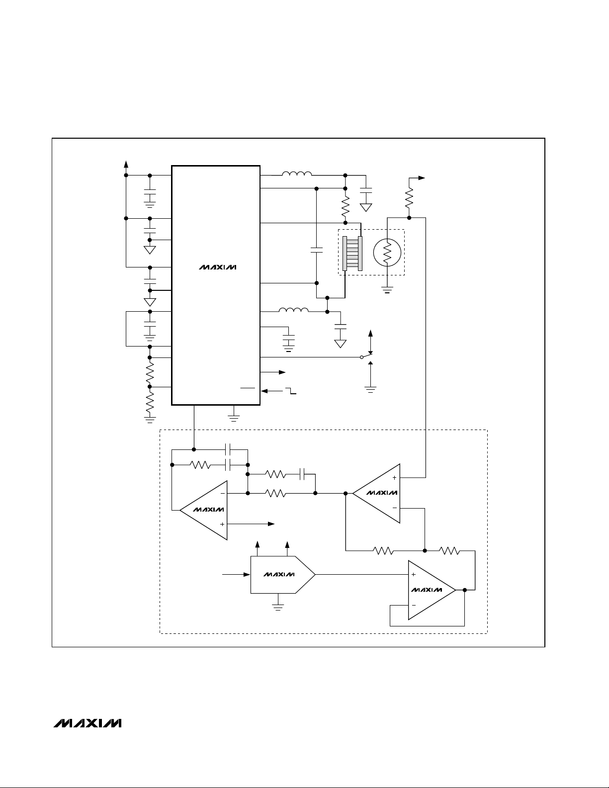
Detailed Description
The MAX8520/MAX8521 TEC drivers consist of two
switching buck regulators that operate together to directly
control the TEC current. This configuration creates a
differential voltage across the TEC, allowing bidirectional
TEC current for controlled cooling and heating. Controlled
cooling and heating allow accurate TEC temperature control to within ±0.01°C. The voltage at CTLI directly sets
the TEC current. An external thermal- control loop is typically used to drive CTLI. Figures 1 and 2 show examples
of the thermal control-loop circuit.
Ripple Cancellation
Switching regulators like those used in the MAX8520/
MAX8521 inherently create ripple voltage on the output.
The dual regulators in the MAX8520/MAX8521 switch in
phase and provide complementary in-phase duty
cycles so ripple waveforms at the TEC are greatly
reduced. This feature suppresses ripple currents and
electrical noise at the TEC to prevent interference with
the laser diode.
Switching Frequency
For the MAX8521, FREQ sets the switching frequency of
the internal oscillator. With FREQ = GND, the oscillator
frequency is set to 500kHz. The oscillator frequency is
1MHz when FREQ = VDD.
For the MAX8520, connect a resistor (R
EXT
in Figure 2)
from FREQ to GND. Choose R
EXT
= 60kΩ for 1MHz
operation, and R
EXT
= 150kΩ for 500kHz operation. For
any intermediary frequency between 500kHz and
1MHz, use the following equation to find the value of
R
EXT
value needed for VDD= 5V:
where R
EXT
is the resistance given in kΩ, and fs is the
desired frequency given in MHz. Note that for VDD<
5V, the frequency is reduced slightly, to the extent of
about 7% when VDDreaches 3V. This should be taken
into consideration when selecting the value for R
EXT
at
a known supply voltage.
Voltage and Current-Limit Setting
Both the MAX8520 and MAX8521 provide control of the
maximum differential TEC voltage. Applying a voltage
to MAXV limits the maximum voltage across the TEC.
The voltage at MAXIP and MAXIN sets the maximum
positive and negative current through the TEC. These
current limits can be independently controlled.
Current Monitor Output
ITEC provides a voltage output proportional to the TEC
current (I
TEC
). See the Functional Diagram for more
details:
V
ITEC
= 1.5V +(8 ✕ (VOS1-VCS))
Reference Output
The MAX8520/MAX8521 include an on-chip voltage reference. The 1.50V reference is accurate to 1% over
temperature. Bypass REF with 0.1µF to GND. REF can
be used to bias an external thermistor for temperature
sensing as shown in Figures 1 and 2.
Thermal and Fault-Current Protection
The MAX8520/MAX8521 provide fault-current protection
in either FET by turning off both high-side and low-side
FETs when the peak current exceeds 3A in either FET. In
addition, thermal-overload protection limits the total
power dissipation in the chip. When the device’s die junction temperature exceeds +165°C, an on-chip thermal
sensor shuts down the device. The thermal sensor turns
the device on again after the junction temperature cools
down by 15°C.
Design Procedures
Duty-Cycle Range Selection
By design, the MAX8520/MAX8521 are capable of operating from 0% to 100% duty cycle, allowing both LX outputs to enter dropout. However, as the LX pulse width
narrows, accurate duty-cycle control becomes difficult.
This can result in a low-frequency noise appearing at the
TEC output (typically in the 20kHz to 50kHz range). While
this noise is typically filtered out by the low thermal-loop
bandwidth, for best results, operate the PWM with a pulse
width greater than 200ns. For a 500kHz application, the
recommended duty-cycle range is from 10% to 90%. For
a 1MHz application, it is from 20% to 80%.
R
fs
EXT
=× −
90
11
3
TEC CONNECTION THERMISTOR
Heating mode PTC
Cooling mode NTC
Table 1. TEC Connection for Figure 1
TEC CONNECTION THERMISTOR
Heating mode NTC
Cooling mode PTC
Table 2. TEC Connection for Figure 2
Page 11
MAX8520/MAX8521
Smallest TEC Power Drivers for
Optical Modules
______________________________________________________________________________________ 11
V
DD
R
SENSE
0.09Ω
C2
1µF
C5
10µF
L2
4.7µF
R2
REF
R
THER
LX1
V
DD
L1
4.7µF
CS
OS1
OS2
PV
DD
1
C1
1µF
C3
1µF
C4
1µF
C6
0.1µF
49.9kΩ
100kΩ
PGND1
PGND2
REF
MAXIP
MAXIN
MAXV
PV
DD
2
MAX8521
LX2
COMP
FREQ
ITEC
ON
OFF
SHDN
CTLI GND
0.022µF
10µF
243kΩ
10kΩ
1µF
510kΩ
100kΩ
10kΩ
TO
U3B
OUTPUT
DAC
INPUTS
V
DD
V
DD
REF
C7
1µF
C8
0.1µF
MAX4477
MAX4477
MAX4475
MAX5144
U1
U2
U4
U3A
U3B
Figure 1. MAX8521 Typical Application Circuit
Page 12

MAX8520/MAX8521
Smallest TEC Power Drivers for
Optical Modules
12 ______________________________________________________________________________________
V
DD
R
SENSE
0.09Ω
C2
1µF
C5
10µF
L2
4.7µF
R2
REF
LX1
V
DD
L1
4.7µF
CS
OS1
OS2
PV
DD
1
C1
1µF
C3
1µF
C4
1µF
C6
0.1µF
49.9kΩ
100kΩ
PGND1
PGND2
REF
MAXIP
MAXIN
MAXV
PV
DD
2
MAX8520
LX2
COMP
FREQ
ITEC
ON
OFF
SHDN
CTLI GND
0.022µF
10µF
243kΩ
1kΩ
10µF
50kΩ
0.01µF
REF
DAC
INPUTS
V
DD
C7
1µF
C8
0.1µF
R
EXT
60kΩ
R
THER
MAX5144
U1
MAX4238
U2
U4
Figure 2. Typical Application Circuit for the MAX8520 with Reduced Op-Amp Count Configuration
Page 13

MAX8520/MAX8521
Smallest TEC Power Drivers for
Optical Modules
______________________________________________________________________________________ 13
Inductor Selection
The MAX8520/MAX8521 dual buck converters operate
in phase and in complementary mode to drive the TEC
differentially in a current-mode control scheme. At zero
TEC current, the differential voltage is zero; hence, the
outputs with respect to GND are equal to half of VDD.
As the TEC current demand increases, one output goes
up and the other goes down from the initial point of
0.5VDDby an amount equal to 0.5 ✕ V
TEC(VTEC
= I
TEC
✕ R
TEC
). Therefore, the operating duty cycle of each
buck converter depends on the operating I
TEC
and
R
TEC
. Since inductor current calculations for heating
and cooling are identical, but reverse in polarity, the
calculations only need to be carried out for either one.
For a given inductor and input voltage, the maximum
inductor ripple current happens when the duty cycle is
at 50%. Therefore, the inductor should be calculated at
50% duty cycle to find the maximum ripple current. The
maximum desired ripple current of a typical standard
buck converter is in the range of 20% to 40% of the
maximum load. The higher the value of the inductor, the
lower the ripple current. However, the size is physically
larger. For the TEC driver, the thermal loop is inherently
slow, so the inductor can be larger for lower ripple
current for better noise and EMI performance. Picking
an inductor to yield ripple current of 10% to 20% of the
maximum TEC current is a good starting point.
Calculate the inductor value as follows:
where LIR is the selected inductor ripple-current ratio,
I
TEC(MAX)
is the maximum TEC current, and fs is the
switching frequency.
As an example, for VDD= 3.3V, LIR = 12%, and fs =
1MHz, L = 4.58µH.
Even though each inductor ripple current is at its maximum at 50% duty cycle (zero TEC current), the ripple
cancels differentially because each is equal and in
phase.
Output Filter Capacitor
Selection
Common-Mode Filter Capacitors
The common-mode filter capacitors (C2 and C7 of Figure
1) are used as filter capacitors to ground for each output.
The output ripple voltage depends on the capacitance,
the ESR of these capacitors, and the inductor ripple
current. Ceramic capacitors are recommended for their
low ESR and impedance at high frequency.
L
V
LIR I fs
DD
TEC MAX
=
×
()
××
025.
()
CTLI
R
SENSE
CS
REF
OS1
C
COMP
R
R
0.5X
REF
1.2X
COMP
PWM
4X
LX2
3/4 V
DD
1/4 V
DD
LX1
-1.2
+1.2
10X
1
gm
Figure 3. Functional Diagram of the Current-Control Loop
Page 14

MAX8520/MAX8521
The output common-mode ripple voltage can be calculated as follows:
V
RIPPLE(P-P)
= LIR x I
TEC(MAX)
(ESR + 1/8 x C x fs)
A 1µF ceramic capacitor with ESR of 10mΩ with LIR =
12% and I
TEC(MAX)
= 1.5A results in V
RIPPLE(P-P)
of
24.3mV. For size-constraint applications, the capacitor
can be made smaller at the expense of higher ripple
voltage. However, the capacitance must be high
enough so that the LC resonant frequency is less than
1/5 the switching frequency:
where f is the resonant frequency of the output filter.
Differential Mode Filter Capacitor
The differential-mode filter capacitor (C5 in Figure 1) is
used to bypass differential ripple current through the
TEC as the result of unequal duty cycle of each output.
This happens when the TEC current is not at zero. As
TEC current increases from zero, both outputs move
away from the 50% duty-cycle point complementarily.
The common-mode ripple decreases, but the differential
ripple does not cancel perfectly, and there is a resulting
differential ripple. The maximum value happens when
one output is at 75% duty cycle and the other is at 25%
duty cycle. At this operating point, the differential ripple
is equal to 1/2 of the maximum common-mode ripple.
The TEC ripple current determines the TEC performance, because the maximum temperature differential
that can be created between the terminals of the TEC
depends on the ratio of ripple current and DC current.
The lower the ripple current, the closer to the ideal
maximum. The differential-mode capacitor provides a
low-impedance path for the ripple current to flow, so that
the TEC ripple current is greatly reduced. The TEC ripple
current can then be calculated as follows:
I
TEC(RIPPLE)
= (0.5 x LIR x I
TEC(MAX)
) x (ZC5)/(R
TEC
+ R
SENSE
+ ZC5)
where ZC5is the impedance of C5 at twice the switching
frequency, R
TEC
is the TEC equivalent resistance, and
R
SENSE
is the current-sense resistor.
Decoupling Capacitor Selection
Decouple each power-supply input (VDD, PVDD1,
PVDD2) with a 1µF ceramic capacitor close to the supply
pins. In applications with long distances between the
source supply and the MAX8520/MAX8521, additional
bypassing may be needed to stabilize the input supply.
In such cases, a low-ESR electrolytic or ceramic capacitor of 100µF or more at V
DD
is sufficient.
Compensation Capacitor
A compensation capacitor is needed to ensure currentcontrol-loop stability (see Figure 3). Select the capacitor
so that the unity-gain bandwidth of the current-control
loop is less than or equal to 10% the resonant frequency
of the output filter:
where:
fBW= unity-gain bandwidth frequency, less than or
equal to 10% the output filter resonant frequency
g
m
= loop transconductance, typically 100µA/V
C
COMP
= value of the compensation capacitor
R
TEC
= TEC series resistance; use the minimum resis-
tance value
R
SENSE
= sense resistor
Setting Voltage and Current Limits
Certain TEC parameters must be considered to guarantee
a robust design. These include maximum positive current,
maximum negative current, and the maximum voltage
allowed across the TEC. These limits should be used to
set the MAXIP, MAXIN, and MAXV voltages.
Setting Max Positive and Negative TEC Current
MAXIP and MAXIN set the maximum positive and negative TEC currents, respectively. The default current limit
is ±150mV/R
SENSE
when MAXIP and MAXIN are connected to REF. To set maximum limits other than the
defaults, connect a resistor-divider from REF to GND to
set V
MAXI_
. Use resistors in the 10kΩ to 100kΩ range.
V
MAXI_
is related to ITEC by the following equations:
V
MAXIP
= 10(I
TECP(MAX)
✕ R
SENSE
)
V
MAXIN
= 10(I
TECN(MAX)
✕ R
SENSE
)
where I
TECP(MAX)
is the maximum positive TEC current
and I
TECN(MAX)
is the negative maximum TEC current.
Positive TEC current occurs when CS is less than OS1:
I
TEC
x R
SENSE
= OS1 - CS
when I
TEC
> 0.
I
TEC
✕ R
SENSE
= CS - OS1
when I
TEC
< 0.
C
g
f
R
RR
COMP
m
BW
SENSE
SENSE TEC
≥
×
×
×
24
2π()
fLC=
1
2π
Smallest TEC Power Drivers for
Optical Modules
14 ______________________________________________________________________________________
Page 15

Take care not to exceed the positive or negative current limit on the TEC. Refer to the manufacturer’s data
sheet for these limits.
Setting Max TEC Voltage
Apply a voltage to the MAXV pin to control the maximum
differential TEC voltage. MAXV can vary from 0 to REF.
The voltage across the TEC is four times V
MAXV
and
can be positive or negative:
|V
OS1
- V
OS2
| = 4 x V
MAXV
or VDD, whichever is lower
Set V
MAXV
with a resistor-divider between REF and
GND using resistors from 10kΩ to 100kΩ. V
MAXV
can
vary from 0 to REF.
Control Inputs/Outputs
Output Current Control
The voltage at CTLI directly sets the TEC current. CTLI
is typically driven from the output of a temperature control loop. The transfer function relating current through
the TEC (I
TEC
) and V
CTLI
is given by:
I
TEC
= (V
CTLI
- V
REF
) / (10 ✕ R
SENSE
)
where V
REF
is 1.50V and:
ITEC = (V
OS1
- VCS) / R
SENSE
CTLI is centered around REF (1.50V). I
TEC
is zero when
CTLI = 1.50V. When V
CTLI
> 1.50V, the current flow is
from OS2 to OS1. The voltages on the pins relate as
follows:
V
OS2
> V
OS1
> V
CS
The opposite applies when V
CTLI
< 1.50V current flows
from OS1 to OS2:
V
OS2
< V
OS1
< V
CS
Shutdown Control
The MAX8520/MAX8521 can be placed in a power-saving
shutdown mode by driving SHDN low. When the
MAX8520/MAX8521 are shut down, the TEC is off (OS1
and OS2 decay to GND) and supply current is reduced to
2mA (typ).
ITEC Output
ITEC is a status output that provides a voltage proportional
to the actual TEC current. V
ITEC
= REF when TEC current
is zero. The transfer function for the ITEC output is:
V
ITEC
= 1.50 + 8 ✕ (V
OS1
– VCS)
Use ITEC to monitor the cooling or heating current
through the TEC. For stability, keep the load capacitance on ITEC to less than 150pF.
Applications Information
The MAX8520/MAX8521 typically drive a TEC inside a
thermal-control loop. TEC drive polarity and power are
regulated based on temperature information read from a
thermistor or other temperature-measuring device to
maintain a stable control temperature. Temperature stability of ±0.01°C can be achieved with carefully selected
external components.
There are numerous ways to implement the thermal loop.
Figures 1 and 2 show designs that employ precision op
amps, along with a DAC or potentiometer to set the control temperature. The loop may also be implemented digitally, using a precision A/D to read the thermistor or
other temperature sensor, a microcontroller to implement
the control algorithm, and a DAC (or filtered-PWM signal)
to send the appropriate signal to the MAX8520/MAX8521
CTLI input. Regardless of the form taken by the thermalcontrol circuitry, all designs are similar in that they read
temperature, compare it to a set-point signal, and then
send an error-correcting signal to the MAX8520/
MAX8521 that moves the temperature in the appropriate
direction.
PC Board Layout and Routing
High switching frequencies and large peak currents
make PC board layout a very important part of design.
Good design minimizes excessive EMI and voltage
gradients in the ground plane, both of which can result
in instability or regulation errors. Follow these guidelines for good PC board layout:
1) Place decoupling capacitors as close to the IC pins
as possible.
2) Keep a separate power ground plane, which is connected to PGND1 and PGND2. PVDD1, PVDD2,
PGND1, and PGND2 are noisy points. Connect
decoupling capacitors from PV
DD
s to PGNDs as
directly as possible. Output capacitors C2 and C7
returns are connected to PGND plane.
3) Connect a decoupling capacitor from V
DD
to GND.
Connect GND to a signal ground plane (separate
from the power ground plane above). Other V
DD
decoupling capacitors (such as the input capacitor)
need to be connected to the PGND plane.
4) Connect GND and PGND_ pins together at a single
point, as close as possible to the chip.
5) Keep the power loop, which consists of input
capacitors, output inductors, and capacitors, as
compact and small as possible.
MAX8520/MAX8521
Smallest TEC Power Drivers for
Optical Modules
______________________________________________________________________________________ 15
Page 16
MAX8520/MAX8521
6) To ensure high DC loop gain and minimum loop
error, keep the board layout adjacent to the negative
input pin of the integrator (U2 in Figure1) clean and
free of moisture. Any contamination or leakage
current into this node can act to lower the DC gain of
the integrator, which can degrade the accuracy of
the thermal loop. If space is available, it can also be
helpful to surround the negative input node of the
integrator with a grounded guard ring.
Refer to the MAX8520/MAX8521 evaluation kit for a PC
board layout example.
Chip Information
TRANSISTOR COUNT: 3007
PROCESS: BiCMOS
Smallest TEC Power Drivers for
Optical Modules
16 ______________________________________________________________________________________
20
19
18
17
PV
DD
1
OS1
OS2
CS
16 PV
DD
2
13
12
11
14
15
V
DD
FREQ
PGND2
LX2
GND
4
3
2
1
COMP
SHDN
PGND1
LX1
5ITEC
6
7
8
9
MAXIN
MAXIP
MAXV
REF
10CTLI
MAX8520/
MAX8521
TOP VIEW
THIN QFN
Pin Configurations
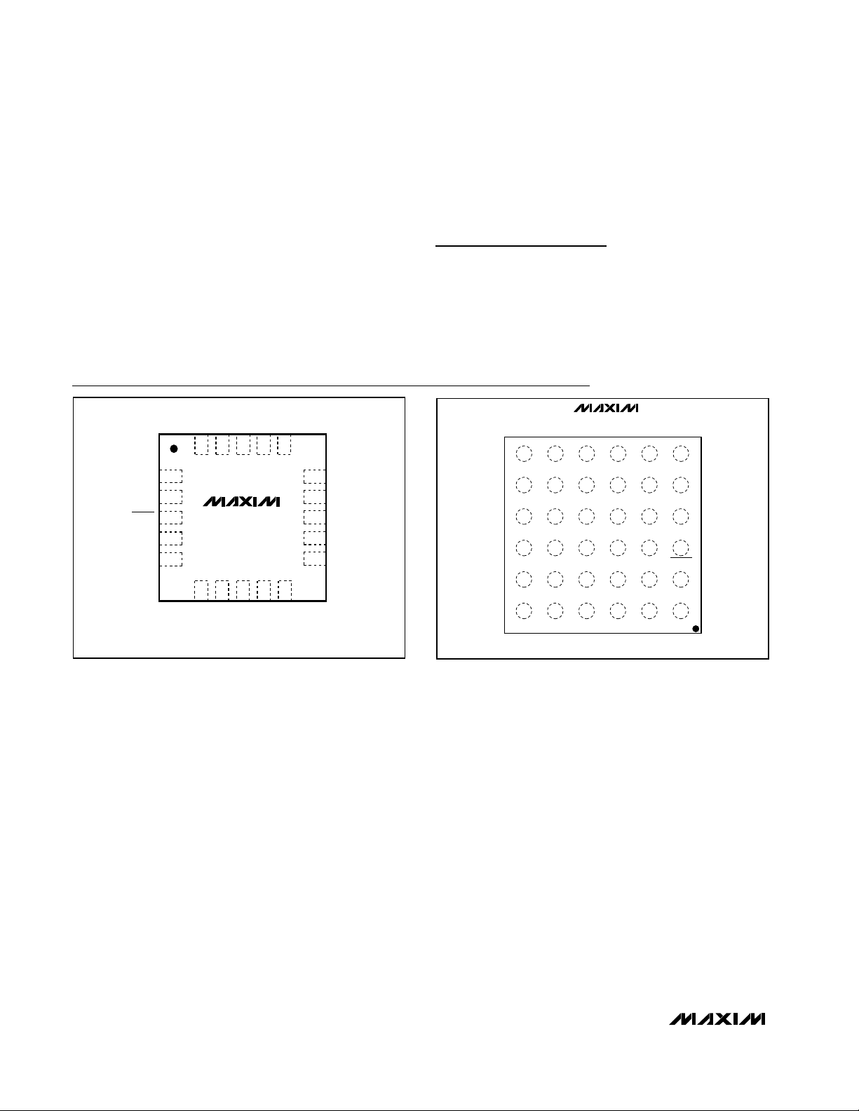
MAX8521
F5 F4 F3 F2 F1
F6
2
PV
E6 E5 E4 E3 E2 E1
LX2 LX2 N.C. N.C. LX1 LX1
D6 D5 D4 D3 D2 D1
PGND2 PGND2 PGND2 PGND1 PGND1 PGND1
C6 C5 C4 C3 C2 C1
OS2 FREQ GND2 GND2 COMP
B6 B5 B4 B3 B2 B1
VDD GND2 N.C. N.C. GND2 ITEC
A6 A5 A4 A3 A2 A1
GND CTLI REF MAXV MAXIP MAXIN
2 CS OS1 PVDD1PVDD1
PV
DD
DD
SHDN
UCSP
Page 17

MAX8520/MAX8521
Smallest TEC Power Drivers for
Optical Modules
______________________________________________________________________________________ 17
GND
FREQ
(MAX8520)
COMP
CTLI
ITEC
MAXIP
FREQ (MAX8521)
PWM CONTROL
AND
GATE CONTROL
MAXIN
R
SENSE
PGND1
PGND2
MAXV
REF
SHDN
REF
OS1
OS2
CS
LX1
LX2
ON
OFF
3V TO
5.5V
OS1
REF
CS
MAX V
TEC
=
V
MAXV
× 4
OR V
DD
MAX I
TEC
=
(V
MAXIP/VREF
) ×
(0.15V/R
SENSE
)
MAX I
TEC
=
(V
MAXIN/VREF
) ×
(0.15V/R
SENSE
)
PV
DD
1
PV
DD
2
V
DD
V
DD
MAX8520/
MAX8521
Functional Diagram
Page 18
MAX8520/MAX8521
Smallest TEC Power Drivers for
Optical Modules
18 ______________________________________________________________________________________
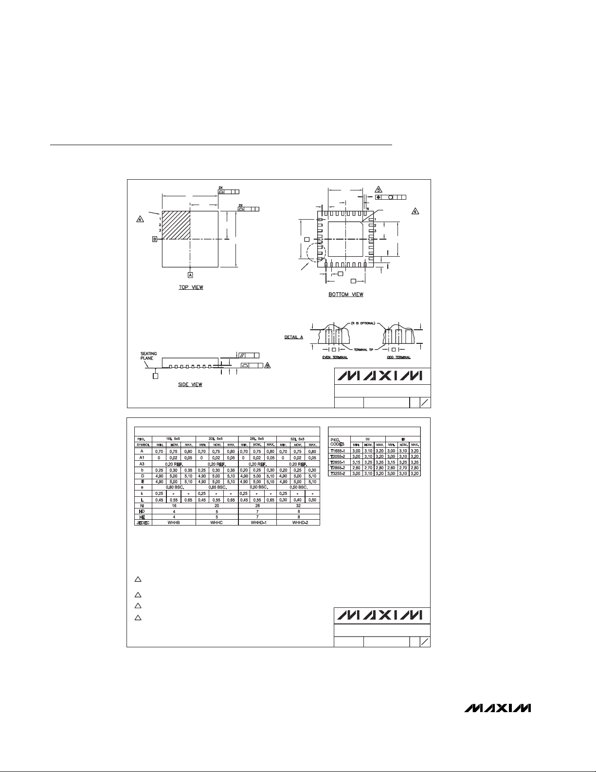
Package Information
(The package drawing(s) in this data sheet may not reflect the most current specifications. For the latest package outline information,
go to www.maxim-ic.com/packages.)
QFN THIN.EPS
D2
(ND-1) X e
e
D
C
PIN # 1
I.D.
(NE-1) X e
E/2
E
0.08 C
0.10
C
A
A1
A3
DETAIL A
0.15
C B
0.15 C A
DOCUMENT CONTROL NO.
21-0140
PACKAGE OUTLINE
16, 20, 28, 32L, QFN THIN, 5x5x0.8 mm
PROPRIETARY INFORMATION
APPROVAL
TITLE:
C
REV.
2
1
E2/2
E2
0.10 M
C A B
PIN # 1 I.D.
b
0.35x45
L
D/2
D2/2
L
C
L
C
e e
L
CC
L
k
k
L
L
2
2
21-0140
REV.DOCUMENT CONTROL NO.APPROVAL
PROPRIETARY INFORMATION
TITLE:
COMMON DIMENSIONS
EXPOSED PAD VARIATIONS
1. DIMENSIONING & TOLERANCING CONFORM TO ASME Y14.5M-1994.
2. ALL DIMENSIONS ARE IN MILLIMETERS. ANGLES ARE IN DEGREES.
3. N IS THE TOTAL NUMBER OF TERMINALS.
4. THE TERMINAL #1 IDENTIFIER AND TERMINAL NUMBERING CONVENTION SHALL CONFORM TO JESD 95-1
SPP-012. DETAILS OF TERMINAL #1 IDENTIFIER ARE OPTIONAL, BUT MUST BE LOCATED WITHIN THE
ZONE INDICATED. THE TERMINAL #1 IDENTIFIER MAY BE EITHER A MOLD OR MARKED FEATURE.
5. DIMENSION b APPLIES TO METALLIZED TERMINAL AND IS MEASURED BETWEEN 0.25 mm AND 0.30 mm
FROM TERMINAL TIP.
6. ND AND NE REFER TO THE NUMBER OF TERMINALS ON EACH D AND E SIDE RESPECTIVELY.
7. DEPOPULATION IS POSSIBLE IN A SYMMETRICAL FASHION.
8. COPLANARITY APPLIES TO THE EXPOSED HEAT SINK SLUG AS WELL AS THE TERMINALS.
9. DRAWING CONFORMS TO JEDEC MO220.
NOTES:
10. WARPAGE SHALL NOT EXCEED 0.10 mm.
C
PACKAGE OUTLINE
16, 20, 28, 32L, QFN THIN, 5x5x0.8 mm
Page 19

MAX8520/MAX8521
Smallest TEC Power Drivers for
Optical Modules
Maxim cannot assume responsibility for use of any circuitry other than circuitry entirely embodied in a Maxim product. No circuit patent licenses are
implied. Maxim reserves the right to change the circuitry and specifications without notice at any time.
Maxim Integrated Products, 120 San Gabriel Drive, Sunnyvale, CA 94086 408-737-7600 ____________________ 19
© 2002 Maxim Integrated Products Printed USA is a registered trademark of Maxim Integrated Products.
Package Information (continued)
(The package drawing(s) in this data sheet may not reflect the most current specifications. For the latest package outline information,
go to www.maxim-ic.com/packages.)
36L,UCSP.EPS
 Loading...