Maxim MAX846AC-D, MAX846AEEE Datasheet

19-1121; Rev 0; 9/96
EVALUATION KIT
AVAILABLE
Cost-Saving Multichemistry
Battery-Charger System
_______________General Description
The MAX846A is a cost-saving multichemistry batterycharger system that comes in a space-saving 16-pin
QSOP. This integrated system allows different battery
chemistries (Li-Ion, NiMH or NiCd cells) to be charged
using one circuit.
In its simplest application, the MAX846A is a standalone, current-limited float voltage source that charges
Li-Ion cells. It can also be paired up with a low-cost
microcontroller (µC) to build a universal charger capable of charging Li-Ion, NiMH, and NiCd cells.
An internal 0.5%-accurate reference allows safe charging of Li-Ion cells that require tight voltage accuracy.
The voltage- and current-regulation loops used to control a low-cost external PNP transistor (or P-channel
MOSFET) are independent of each other, allowing more
flexibility in the charging algorithms.
The MAX846A has a built-in 1%, 3.3V, 20mA linear regulator capable of powering the µC and providing a reference for the µC’s analog-to-digital converters. An
on-board reset notifies the controller upon any unexpected loss of power. The µC can be inexpensive, since
its only functions are to monitor the voltage and current
and to change the charging algorithms.
________________________Applications
Li-Ion Battery Packs
Desktop Cradle Chargers
Li-Ion/NiMH/NiCd Multichemistry Battery
Chargers
Cellular Phones
Notebook Computers
Hand-Held Instruments
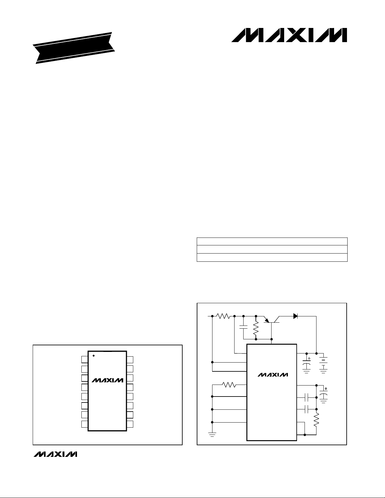
__________________Pin Configuration
TOP VIEW
DCIN
CCI
GND
CCV
VSET
ISET
OFFV
1
VL
2
3
MAX846A
4
5
6
7
8
QSOP
DRV
16
PGND
15
14
CS-
CS+
13
12
BATT
11
ON
10
CELL2
9
PWROK
____________________________Features
♦ Multichemistry Charger System (Li-Ion, NiMH, NiCd)
♦ Independent Voltage and Current Loops
♦ ±0.5% Internal Reference for Li-Ion Cells
♦ Lowers Cost:
—Stands Alone or Uses Low-Cost µC
—Built-In 1% Linear Regulator Powers µC
—Linear Regulator Provides Reference to µC ADCs
—Built-In µC Reset
—Controls Low-Cost External PNP Transistor or
P-Channel MOSFET
♦ Space-Saving 16-Pin QSOP
♦ Charging-Current-Monitor Output
♦ <1µA Battery Drain when Off
______________Ordering Information
PART
MAX846AC/D
MAX846AEEE -40°C to +85°C
*Dice are tested at TA= +25°C only. Contact factory for details.
TEMP. RANGE PIN-PACKAGE
0°C to +70°C
Dice*
16 QSOP
__________Typical Operating Circuit
3.5V
TO
20V
DRV
CSCS+
DCIN
ISET
CELL2
GND
PGND
MAX846A
BATT
CCV
CCI
PWROK
Li-ION
BATTERY
VL
ON
MAX846A
________________________________________________________________
Maxim Integrated Products
1
For free samples & the latest literature: http://www.maxim-ic.com, or phone 1-800-998-8800

Cost-Saving Multichemistry
Battery-Charger System
ABSOLUTE MAXIMUM RATINGS
DCIN, DRV, CS+, CS-, BATT to GND........................-0.3V, +21V
PGND to GND.....................................................................±0.3V
VL to GND......................................................................-0.3V, 7V
................................................................................10mA
I
PWROK
PWROK, ISET, CCI, CCV, OFFV, VSET,
CELL2, ON to GND............................................-0.3V, VL + 0.3V
CS+ to CS-..........................................................................±0.3V
VL Short to GND.........................................................Continuous
...................................................................................100mA
I
DRV
MAX846A
Stresses beyond those listed under “Absolute Maximum Ratings” may cause permanent damage to the device. These are stress ratings only, and functional
operation of the device at these or any other conditions beyond those indicated in the operational sections of the specifications is not implied. Exposure to
absolute maximum rating conditions for extended periods may affect device reliability.
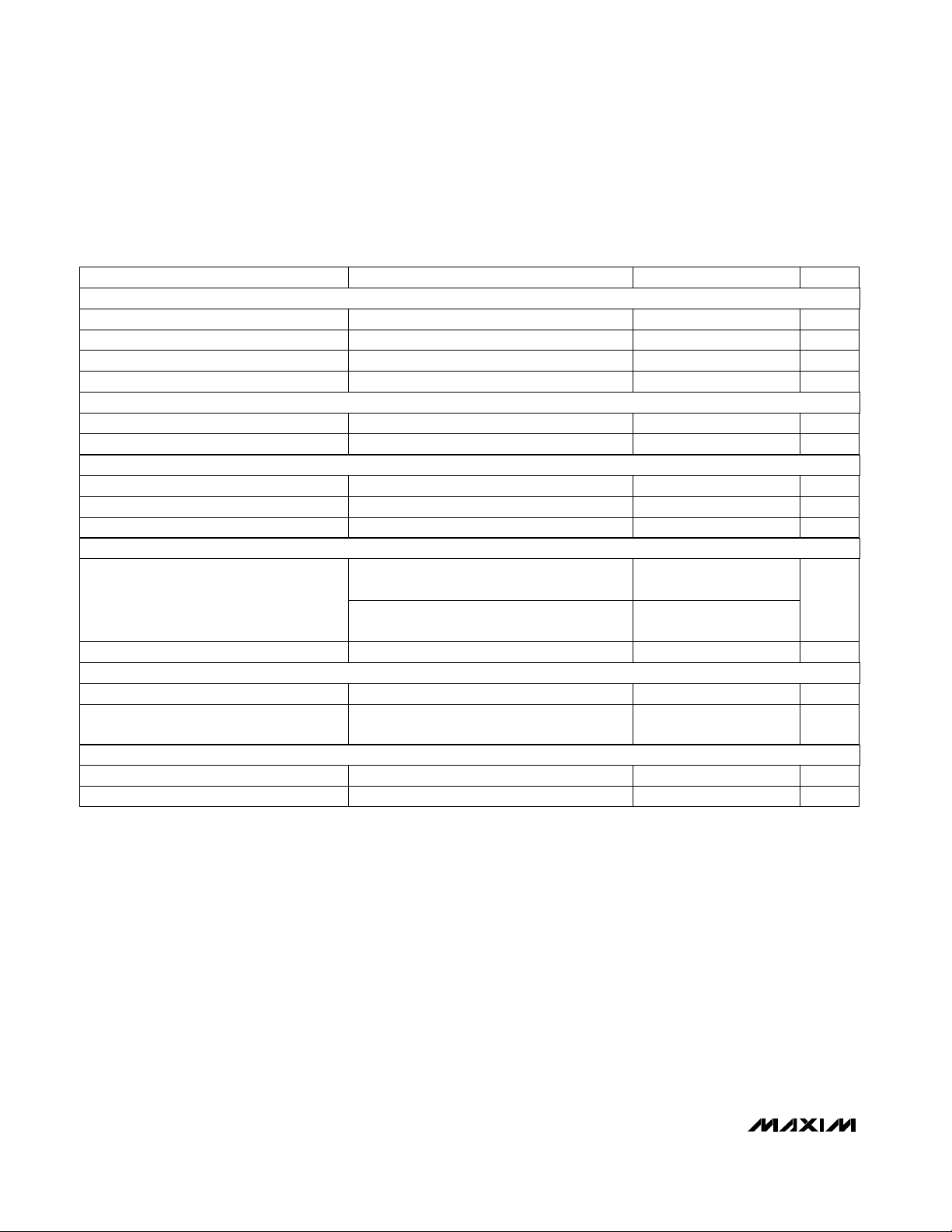
ELECTRICAL CHARACTERISTICS
(V
= 10V, ON = VL, IVL= I
DCIN
otherwise noted. Typical values are at T
VL REGULATOR
REFERENCE
Output Voltage
CURRENT-SENSE AMPLIFIER
Transconductance V
Output Offset Current V
Input Common-Mode Range Measured at V
Maximum Differential Input Voltage
CS- Lockout Voltage
CS+, CS- Input Current V
CS+, CS- Off Input Current DCIN = VL = ON = GND 0.01 10
= 0mA, VCS- = V
VSET
A
= 10V, V
= +25°C.)
CS+
V
= 20V, I
DCIN
0mA < IVL< 20mA, 3.7V < V
VL = GND
Rising VL edge, 2% hysteresis
Measured at VSET, I
= 1.7V, V
ISET
= 4V 3
CS+
V
= V
CS-
CSA transconductance >0.9mA/V
When V
disabled.
CS+
= 2.1V,
ISET
is less than this voltage, DRV is
CS-
= 20V, V
Continuous Power Dissipation (T
QSOP (derate 8.3mW/°C above +70°C)........................667mW
Operating Temperature Range
MAX846AEEE ....................................................-40°C to +85°C
Junction Temperature......................................................+150°C
Storage Temperature Range.............................-65°C to +160°C
Lead Temperature (soldering, 10sec).............................+300°C
= 4.5V, V
BATT
CONDITIONS
= IVL= 0mA mA5DCIN Supply Current
DRV
VSET
- V
CS+
CS-
, V
- V
CS+
CS-
CS+-VCS-
= 165mV 250
DCIN
= 0mA, VON= 0V
= 165mV 0.95 1 1.05 mA/V
CS-
= V
OFFV
< 20V
= 165mV 2.1 20.0 V
= 0V, TA= 0°C to +85°C, unless
CELL2
= +70°C)
A
225 mV
1.9 2.1 V
UNITSMIN TYP MAXPARAMETER
V3.7 20.0Operating Range
V3.267 3.305 3.333Output Voltage
mA50Short-Circuit Current Limit
V2.9 3.0 3.1PWROK Trip Level
V2.5 2.9VL Undervoltage-Lockout Level
V-0.5% 1.650 +0.5%
kΩ-2% 20 +2%Output Resistance
µA
µA
µA
2 _______________________________________________________________________________________

Cost-Saving Multichemistry
Battery-Charger System
ELECTRICAL CHARACTERISTICS (continued)
(V
= 10V, ON = VL, IVL= I
DCIN
otherwise noted. Typical values are at T
VOLTAGE LOOP
Voltage-Loop Set Point
BATT Input Current
CURRENT LOOP
Current-Loop Set Point I
CA Voltage Gain 5
CCI Output Impedance 50 kΩ
Overcurrent Trip Level
DRIVER
DRV Sink Current V
DRV Off Current V
LOGIC INPUTS AND OUTPUTS
Input High Level CELL2, ON, OFFV 2.4 VL V
Input Low Level CELL2, ON, OFFV 0 0.8 V
Input Current CELL2, ON, OFFV 0.01 1
PWROK Output Low Level I
PWROK Output High Leakage V
= 0mA, VCS- = V
VSET
A
= +25°C.)
V
VSET
V
DRV
V
VSET
V
DRV
1mA < I
V
BATT
V
BATT
DRV
When V
is disabled.
DRV
DRV
PWROK
PWROK
= 10V, V
CS+
= 1.650V, V
= 10V
= 1.650V, V
= 10V
< 5mA
DRV
= 10V, CELL2 = GND or VL
= 10V, ON = GND, CELL2 = GND or VL
= 5mA, V
= 3V 20 mA
= 20V, VON= 0V 0.1 100
DRV
exceeds this voltage, DRV current
ISET
= 1mA, V
= 3.3V 0.01 1
= 4.5V, V
BATT
CONDITIONS
= 0V, I
CELL2
CELL2
= 10V
DCIN
DRV
= VL, I
DRV
= VVL= 2.5V 0.4 V
= V
OFFV
= 1mA,
= 1mA,
MAX846A
= 0V, TA= 0°C to +85°C, unless
CELL2
-0.25% 4.2 +0.25%
-0.25% 8.4 +0.25%
0.05Voltage-Loop Load Regulation
0.01 1BATT Off Input Current
1.634 1.650 1.666 V
1.90 2.1 V
225
MAX846A
UNITSMIN TYP MAXPARAMETER
V
V1.25 2.0VSET Common-Mode Input Range
kΩ150CCV Output Impedance
%
µA
µA
V/V
µA
µA
µA
_______________________________________________________________________________________ 3

Cost-Saving Multichemistry
Battery-Charger System
ELECTRICAL CHARACTERISTICS (Note 1)
(V
= 10V, ON = VL, IVL= I
DCIN
otherwise noted.)
= 0mA, VCS- = V
VSET
CS+
= 10V, V
BATT
= 4.5V, V
OFFV
= V
= 0V, TA= -40°C to +85°C, unless
CELL2
CONDITIONS
VL REGULATOR
V
DCIN
= 20V, I
DRV
= IVL= 0mA mA5DCIN Supply Current
0mA < IVL< 20mA, 3.7V < V
MAX846A
Rising VL edge, 2% hysteresis
REFERENCE
Measured at VSET, I
= 0mA, VON= 0V
VSET
CURRENT-SENSE AMPLIFIER
Transconductance V
Output Offset Current V
CS+, CS- Off Input Current V
ISET
CS+
ON
= 1.7V, V
= 4V
= 0V, V
CS+
CS+
= V
- V
= 165mV
CS-
= 10V 10
CS-
VOLTAGE LOOP
V
Voltage-Loop Set Point
BATT Off Input Current V
= 1.650V, V
VSET
V
= 10V
DRV
V
= 1.650V, V
VSET
V
= 10V
DRV
= 10V, ON = GND, CELL2 = GND or VL 1
BATT
CELL2
CELL2
= 0V, I
= VL, I
CURRENT LOOP
Current-Loop Set Point I
Overcurrent Trip Level
= 5mA, V
DRV
When V
ISET
is disabled.
= 10V 1.625 1.675 V
DRV
exceeds this voltage, DRV current
DRIVER
DRV Sink Current V
DRV Off Current
= 3V 20 mA
DRV
V
= 20V, ON = GND 100
DRV
Note 1: Specifications to -40°C are guaranteed by design and not production tested.
< 20V
DCIN
= 1mA,
DRV
MAX846A
= 1mA,
DRV
UNITSMIN TYP MAXPARAMETER
-2% 20 +2%Output Resistance
kΩ
0.93 1.07 mA/V
5
µA
µA
-0.35% 4.2 +0.35%
-0.35% 8.4 +0.35%
µA
1.86 2.14 V
µA
V3.259 3.341Output Voltage
V2.9 3.1PWROK Trip Level
V2.5 3.0VL Undervoltage-Lockout Level
V-0.7% 1.650 +0.7%Output Voltage
V
4 _______________________________________________________________________________________
 Loading...