

19-1121; Rev 0; 9/96
EVALUATION KIT
AVAILABLE
Cost-Saving Multichemistry
Battery-Charger System
_______________General Description
The MAX846A is a cost-saving multichemistry batterycharger system that comes in a space-saving 16-pin
QSOP. This integrated system allows different battery
chemistries (Li-Ion, NiMH or NiCd cells) to be charged
using one circuit.
In its simplest application, the MAX846A is a standalone, current-limited float voltage source that charges
Li-Ion cells. It can also be paired up with a low-cost
microcontroller (µC) to build a universal charger capable of charging Li-Ion, NiMH, and NiCd cells.
An internal 0.5%-accurate reference allows safe charging of Li-Ion cells that require tight voltage accuracy.
The voltage- and current-regulation loops used to control a low-cost external PNP transistor (or P-channel
MOSFET) are independent of each other, allowing more
flexibility in the charging algorithms.
The MAX846A has a built-in 1%, 3.3V, 20mA linear regulator capable of powering the µC and providing a reference for the µC’s analog-to-digital converters. An
on-board reset notifies the controller upon any unexpected loss of power. The µC can be inexpensive, since
its only functions are to monitor the voltage and current
and to change the charging algorithms.
________________________Applications
Li-Ion Battery Packs
Desktop Cradle Chargers
Li-Ion/NiMH/NiCd Multichemistry Battery
Chargers
Cellular Phones
Notebook Computers
Hand-Held Instruments
__________________Pin Configuration
TOP VIEW
DCIN
CCI
GND
CCV
VSET
ISET
OFFV
1
VL
2
3
MAX846A
4
5
6
7
8
QSOP
DRV
16
PGND
15
14
CS-
CS+
13
12
BATT
11
ON
10
CELL2
9
PWROK
____________________________Features
♦ Multichemistry Charger System (Li-Ion, NiMH, NiCd)
♦ Independent Voltage and Current Loops
♦ ±0.5% Internal Reference for Li-Ion Cells
♦ Lowers Cost:
—Stands Alone or Uses Low-Cost µC
—Built-In 1% Linear Regulator Powers µC
—Linear Regulator Provides Reference to µC ADCs
—Built-In µC Reset
—Controls Low-Cost External PNP Transistor or
P-Channel MOSFET
♦ Space-Saving 16-Pin QSOP
♦ Charging-Current-Monitor Output
♦ <1µA Battery Drain when Off
______________Ordering Information
PART
MAX846AC/D
MAX846AEEE -40°C to +85°C
*Dice are tested at TA= +25°C only. Contact factory for details.
TEMP. RANGE PIN-PACKAGE
0°C to +70°C
Dice*
16 QSOP
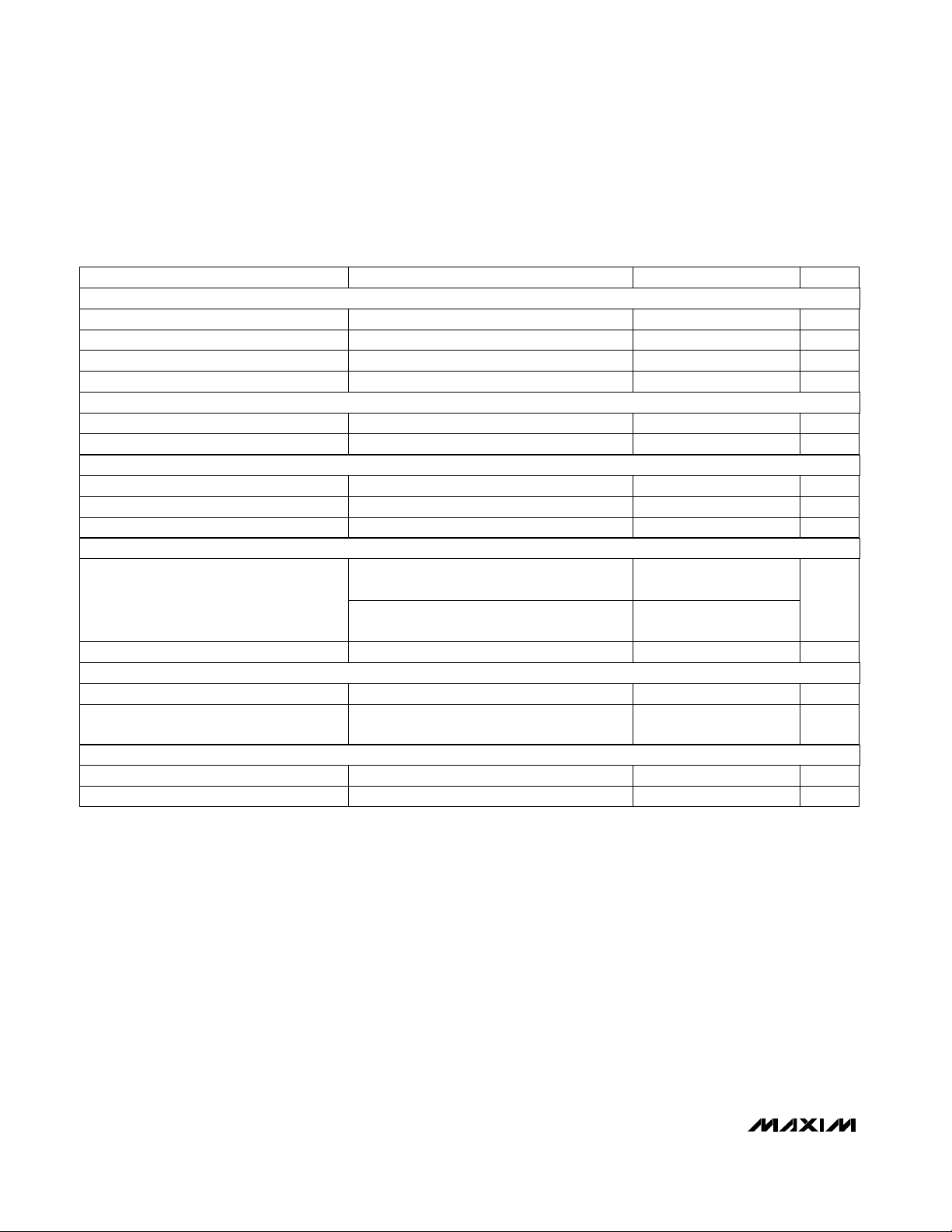
__________Typical Operating Circuit
3.5V
TO
20V
DRV
CSCS+
DCIN
ISET
CELL2
GND
PGND
MAX846A
BATT
CCV
CCI
PWROK
Li-ION
BATTERY
VL
ON
MAX846A
________________________________________________________________
Maxim Integrated Products
1
For free samples & the latest literature: http://www.maxim-ic.com, or phone 1-800-998-8800

Cost-Saving Multichemistry
Battery-Charger System
ABSOLUTE MAXIMUM RATINGS
DCIN, DRV, CS+, CS-, BATT to GND........................-0.3V, +21V
PGND to GND.....................................................................±0.3V
VL to GND......................................................................-0.3V, 7V
................................................................................10mA
I
PWROK
PWROK, ISET, CCI, CCV, OFFV, VSET,
CELL2, ON to GND............................................-0.3V, VL + 0.3V
CS+ to CS-..........................................................................±0.3V
VL Short to GND.........................................................Continuous
...................................................................................100mA
I
DRV
MAX846A
Stresses beyond those listed under “Absolute Maximum Ratings” may cause permanent damage to the device. These are stress ratings only, and functional
operation of the device at these or any other conditions beyond those indicated in the operational sections of the specifications is not implied. Exposure to
absolute maximum rating conditions for extended periods may affect device reliability.
ELECTRICAL CHARACTERISTICS
(V
= 10V, ON = VL, IVL= I
DCIN
otherwise noted. Typical values are at T
VL REGULATOR
REFERENCE
Output Voltage
CURRENT-SENSE AMPLIFIER
Transconductance V
Output Offset Current V
Input Common-Mode Range Measured at V
Maximum Differential Input Voltage
CS- Lockout Voltage
CS+, CS- Input Current V
CS+, CS- Off Input Current DCIN = VL = ON = GND 0.01 10
= 0mA, VCS- = V
VSET
A
= 10V, V
= +25°C.)
CS+
V
= 20V, I
DCIN
0mA < IVL< 20mA, 3.7V < V
VL = GND
Rising VL edge, 2% hysteresis
Measured at VSET, I
= 1.7V, V
ISET
= 4V 3
CS+
V
= V
CS-
CSA transconductance >0.9mA/V
When V
disabled.
CS+
= 2.1V,
ISET
is less than this voltage, DRV is
CS-
= 20V, V
Continuous Power Dissipation (T
QSOP (derate 8.3mW/°C above +70°C)........................667mW
Operating Temperature Range
MAX846AEEE ....................................................-40°C to +85°C
Junction Temperature......................................................+150°C
Storage Temperature Range.............................-65°C to +160°C
Lead Temperature (soldering, 10sec).............................+300°C
= 4.5V, V
BATT
CONDITIONS
= IVL= 0mA mA5DCIN Supply Current
DRV
VSET
- V
CS+
CS-
, V
- V
CS+
CS-
CS+-VCS-
= 165mV 250
DCIN
= 0mA, VON= 0V
= 165mV 0.95 1 1.05 mA/V
CS-
= V
OFFV
< 20V
= 165mV 2.1 20.0 V
= 0V, TA= 0°C to +85°C, unless
CELL2
= +70°C)
A
225 mV
1.9 2.1 V
UNITSMIN TYP MAXPARAMETER
V3.7 20.0Operating Range
V3.267 3.305 3.333Output Voltage
mA50Short-Circuit Current Limit
V2.9 3.0 3.1PWROK Trip Level
V2.5 2.9VL Undervoltage-Lockout Level
V-0.5% 1.650 +0.5%
kΩ-2% 20 +2%Output Resistance
µA
µA
µA
2 _______________________________________________________________________________________

Cost-Saving Multichemistry
Battery-Charger System
ELECTRICAL CHARACTERISTICS (continued)
(V
= 10V, ON = VL, IVL= I
DCIN
otherwise noted. Typical values are at T
VOLTAGE LOOP
Voltage-Loop Set Point
BATT Input Current
CURRENT LOOP
Current-Loop Set Point I
CA Voltage Gain 5
CCI Output Impedance 50 kΩ
Overcurrent Trip Level
DRIVER
DRV Sink Current V
DRV Off Current V
LOGIC INPUTS AND OUTPUTS
Input High Level CELL2, ON, OFFV 2.4 VL V
Input Low Level CELL2, ON, OFFV 0 0.8 V
Input Current CELL2, ON, OFFV 0.01 1
PWROK Output Low Level I
PWROK Output High Leakage V
= 0mA, VCS- = V
VSET
A
= +25°C.)
V
VSET
V
DRV
V
VSET
V
DRV
1mA < I
V
BATT
V
BATT
DRV
When V
is disabled.
DRV
DRV
PWROK
PWROK
= 10V, V
CS+
= 1.650V, V
= 10V
= 1.650V, V
= 10V
< 5mA
DRV
= 10V, CELL2 = GND or VL
= 10V, ON = GND, CELL2 = GND or VL
= 5mA, V
= 3V 20 mA
= 20V, VON= 0V 0.1 100
DRV
exceeds this voltage, DRV current
ISET
= 1mA, V
= 3.3V 0.01 1
= 4.5V, V
BATT
CONDITIONS
= 0V, I
CELL2
CELL2
= 10V
DCIN
DRV
= VL, I
DRV
= VVL= 2.5V 0.4 V
= V
OFFV
= 1mA,
= 1mA,
MAX846A
= 0V, TA= 0°C to +85°C, unless
CELL2
-0.25% 4.2 +0.25%
-0.25% 8.4 +0.25%
0.05Voltage-Loop Load Regulation
0.01 1BATT Off Input Current
1.634 1.650 1.666 V
1.90 2.1 V
225
MAX846A
UNITSMIN TYP MAXPARAMETER
V
V1.25 2.0VSET Common-Mode Input Range
kΩ150CCV Output Impedance
%
µA
µA
V/V
µA
µA
µA
_______________________________________________________________________________________ 3
Cost-Saving Multichemistry
Battery-Charger System
ELECTRICAL CHARACTERISTICS (Note 1)
(V
= 10V, ON = VL, IVL= I
DCIN
otherwise noted.)
= 0mA, VCS- = V
VSET
CS+
= 10V, V
BATT
= 4.5V, V
OFFV
= V
= 0V, TA= -40°C to +85°C, unless
CELL2
CONDITIONS
VL REGULATOR
V
DCIN
= 20V, I
DRV
= IVL= 0mA mA5DCIN Supply Current
0mA < IVL< 20mA, 3.7V < V
MAX846A
Rising VL edge, 2% hysteresis
REFERENCE
Measured at VSET, I
= 0mA, VON= 0V
VSET
CURRENT-SENSE AMPLIFIER
Transconductance V
Output Offset Current V
CS+, CS- Off Input Current V
ISET
CS+
ON
= 1.7V, V
= 4V
= 0V, V
CS+
CS+
= V
- V
= 165mV
CS-
= 10V 10
CS-
VOLTAGE LOOP
V
Voltage-Loop Set Point
BATT Off Input Current V
= 1.650V, V
VSET
V
= 10V
DRV
V
= 1.650V, V
VSET
V
= 10V
DRV
= 10V, ON = GND, CELL2 = GND or VL 1
BATT
CELL2
CELL2
= 0V, I
= VL, I
CURRENT LOOP
Current-Loop Set Point I
Overcurrent Trip Level
= 5mA, V
DRV
When V
ISET
is disabled.
= 10V 1.625 1.675 V
DRV
exceeds this voltage, DRV current
DRIVER
DRV Sink Current V
DRV Off Current
= 3V 20 mA
DRV
V
= 20V, ON = GND 100
DRV
Note 1: Specifications to -40°C are guaranteed by design and not production tested.
< 20V
DCIN
= 1mA,
DRV
MAX846A
= 1mA,
DRV
UNITSMIN TYP MAXPARAMETER
-2% 20 +2%Output Resistance
kΩ
0.93 1.07 mA/V
5
µA
µA
-0.35% 4.2 +0.35%
-0.35% 8.4 +0.35%
µA
1.86 2.14 V
µA
V3.259 3.341Output Voltage
V2.9 3.1PWROK Trip Level
V2.5 3.0VL Undervoltage-Lockout Level
V-0.7% 1.650 +0.7%Output Voltage
V
4 _______________________________________________________________________________________

Cost-Saving Multichemistry
Battery-Charger System
__________________________________________Typical Operating Characteristics
(TA = +25°C, unless otherwise noted.)
CURRENT-SENSE AMPLIFIER
TRANSCONDUCTANCE vs. ISET VOLTAGE
1.035
∆V = V
1.030
1.025
1.020
1.015
1.010
CSA GM (mA/V)
1.005
1.000
0.995
0.990
0 0.4 1.2 2.0
- V
CS+
∆V = 100mV
∆V = 200mV
CS-
∆V = 165mV
∆V = 250mV
0.8 1.60.2 1.0 1.80.6 1.4
ISET VOLTAGE (V)
CURRENT-LOOP GAIN
80
C
= 10nF
CCI
70
60
50
40
30
GAIN (dB)
20
10
0
-10
-20
10 10k 100k1k100 1M
GAIN
PHASE
FREQUENCY (Hz)
MAX846-01
MAX846-03
180
150
120
90
60
30
0
PHASE (DEGREES)
-30
-60
-90
-120
Li-ION CHARGING PROFILE
900
800
700
600
500
400
300
CHARGING CURRENT (mA)
200
100
0
0 180 24012060
TIME (MINUTES)
80
70
60
50
40
30
20
BATT INPUT CURRENT (µA)
10
40
30
20
10
-10
GAIN (dB)
-20
-30
-40
-50
-60
MAX846-04
BATTERY VOLTAGE
CHARGING CURRENT
0
0
BATTERY INPUT CURRENT
vs. BATTERY VOLTAGE
CELL2 = VL
CELL2 = GND
82kΩ
ON
02 6 10
4815 937
BATT VOLTAGE (V)
128kΩ
OFF
MAX846-02
VOLTAGE-LOOP GAIN
GAIN
= - Charging at 100mA
= -Charging at 200mA
2 Li-Ion Cells
C
= 10nF
CCV
C
= 4.7µF
OUT
TIP2955 PNP PASS TRANSISTOR
10 10k 100k1k100 1M
FREQUENCY (Hz)
9.0
8.8
8.6
8.4
8.2
8.0
7.8
7.6
BATTERY VOLTAGE (V)
7.4
7.2
7.0
PHASE
MAX846-04
180
150
120
90
60
30
0
-30
-60
-90
--120
PHASE (DEGREES)
MAX846A
_______________________________________________________________________________________
5

Cost-Saving Multichemistry
Battery-Charger System
______________________________________________________________Pin Description
PIN FUNCTION
1 Supply Input from External DC Source. 3.7V ≤ V
2
MAX846A
3
4 Ground
5
6
7 ISET
8 OFFV Logic Input that disables the voltage-regulation loop. Set OFFV high for NiCd or NiMH batteries.
9 PWROK
10 CELL2
11 ON
12 BATT Battery Input. Connect BATT to positive battery terminal.
13 CS+
14 CS- Current-Sense Amplifier Low-Side Input. Connect CS- to the sense resistor’s battery side.
15 PGND Power Ground
16 DRV External Pass Transistor (P-channel MOSFET or PNP) Base/Gate Drive Output. DRV sinks current only.
NAME
DCIN
VL
CCI
GND
CCV
VSET
3.3V, 20mA, 1% Linear-Regulator Output. VL powers the system µC and other components. Bypass to
GND with a 4.7µF tantalum or ceramic capacitor.
Current-Regulation-Loop Compensation Pin. Connect a compensation capacitor (typically 10nF) from
CCI to VL.
Voltage-Regulation-Loop Compensation Pin. Connect a compensation capacitor (typically 10nF) from
CCV to VL.
Float-Voltage Reference-Adjust Input. Leave VSET open for a 4.2V default. See the
Information
Current-Set Input/Current-Monitor Output. ISET sets the current-regulation point. Connect a resistor
from ISET to GND to monitor the charging current. ISET voltage is regulated at 1.65V by the currentregulation loop. To adjust the current-regulation point, either modify the resistance from ISET to ground
or connect a fixed resistor and adjust the voltage on the other side of the resistor (Figure 5). The
transconductance of the current-sense amplifier is 1mA/V.
Open-Drain, Power-Good Output to µC. PWROK is low when VL is less than 3V. The reset timeout period can be set externally using an RC circuit (Figure 3).
Digital Input. CELL2 programs the number of Li-Ion cells to be charged. A high level equals two cells; a
low level equals one cell.
Charger ON/OFF Input. When low, the driver section is turned off and I
always active.
Current-Sense Amplifier High-Side Input. Connect CS+ to the sense resistor’s power-source side. The
sense resistor may be placed on either side of the pass transistor.
section for adjustment information.
DCIN
≤ 20V.
Applications
<1µA. The VL regulator is
BATT
_______________Detailed Description
The MAX846A battery-charging controller combines
three functional blocks: a 3.3V precision, low-dropout
linear regulator (LDO), a precision voltage reference,
and a voltage/current regulator (Figure 1).
Linear Regulator
The LDO regulator output voltage (VL) is two times the
internal reference voltage; therefore, the reference and
LDO track. VL delivers up to 20mA to an external load
and is short-circuit protected. The power-good output
The precision internal reference provides a voltage to
accurately set the float voltage for lithium-ion (Li-Ion)
battery charging. The reference output connects in
series with an internal, 2%-accurate, 20kΩ resistor. This
allows the float voltage to be adjusted using one external 1% resistor (R
VSET
(Figure 4). The float-voltage accuracy is important for
battery life and to ensure full capacity in Li-Ion batteries. Table 1 shows the accuracies attainable using the
MAX846A.
Voltage Reference
) to form a voltage divider
(PWROK) provides microcontroller (µC) reset and
charge-current inhibition.
6 _______________________________________________________________________________________

Cost-Saving Multichemistry
Battery-Charger System
Voltage/Current Regulator
The voltage/current regulator consists of a precision
attenuator, voltage loop, current-sense amplifier, and
current loop. The attenuator can be pin programmed to
set the regulation voltage for one or two Li-Ion cells
(4.2V and 8.4V, respectively). The current-sense amplifier is configured to sense the battery current on the
high side. It is, in essence, a transconductance amplifier converting the voltage across an external sense
resistor (RCS) to a current, and applying this current to
an external load resistor (R
by selecting RCSand R
also be adjusted by varying the voltage at the low side
of R
ISET node (Figure 5). The voltage and current loops are
individually compensated using external capacitors at
CCV and CCI, respectively. The outputs of these two
loops are OR’ed together and drive an open-drain,
internal N-channel MOSFET transistor sinking current to
ground. An external P-channel MOSFET or PNP transistor pass element completes the loop.
or by summing/subtracting current from the
ISET
). Set the charge current
ISET
. The charge current can
ISET
Stability
The
Typical Operating Characteristics
gains for the current loop and voltage loop. The dominant pole for each loop is set by the compensation
capacitor connected to each capacitive compensation
pin (CCI, CCV). The DC loop gains are about 50dB for
the current loop and about 33dB for the voltage loop,
for a battery impedance of 250mΩ.
The CCI output impedance (50kΩ) and the CCI capacitor determine the current-loop dominant pole. In Figure
2, the recommended C
dominant pole at 300Hz. There is a high-frequency
pole, due to the external PNP, at approximately fT/ß.
This pole frequency (on the order of a few hundred kilohertz) will vary with the type of PNP used. Connect a
10nF capacitor between the base and emitter of the
is 10nF, which places a
CCV
show the loop
PNP to prevent self-oscillation (due to the high-impedance base drive).
Similarly, the CCV output impedance (150kΩ) and the
CCV capacitor set the voltage-loop dominant pole. In
Figure 2, the compensation capacitance is 10nF, which
places a dominant pole at 200Hz.
The battery impedance directly affects the voltage-loop
DC and high-frequency gain. At DC, the loop gain is
proportional to the battery resistance. At higher frequencies, the AC impedance of the battery and its connections introduces an additional high-frequency zero.
A 4.7µF output capacitor in parallel with the battery,
mounted close to BATT, minimizes the impact of this
impedance. The effect of the battery impedance on DC
gain is noticeable in the Voltage-Loop-Gain graph (see
Typical Operating Characteristics
sents voltage-loop gain versus frequency for a fully
charged battery, when the battery energy level is high
and the ESR is low. The charging current is 100mA. The
dashed line shows the loop gain with a 200mA charging current, a lower amount of stored energy in the battery, and a higher battery ESR.
). The solid line repre-
__________Applications Information
Stand-Alone Li-Ion Charger
Figure 2 shows the stand-alone configuration of the
MAX846A. Select the external components and pin
configurations as follows:
• Program the number of cells: Connect CELL2 to GND
for one-cell operation, or to VL for two-cell operation.
• Program the float voltage: Connect a 1% resistor from
VSET to GND to adjust the float voltage down, or to
VL to adjust it up. If VSET is unconnected, the float
voltage will be 4.2V per cell. Let the desired float voltage per cell be VF, and calculate the resistor value
as follows:
MAX846A
Table 1. Float-Voltage Accuracy
ERROR SOURCE ERROR
VSET error due to external divider. Calculated from a 2% internal 20kΩ resistor tolerance and
a 1% external R
adjustment range of 5%.
resistor tolerance. The total error is 3% x (adjustment). Assume max
VSET
_______________________________________________________________________________________ 7
±0.5%Internal-reference accuracy
±0.15%
±0.25%VSET amplifier and divider accuracy
±0.9%TOTAL

Cost-Saving Multichemistry
Battery-Charger System
DC INPUT (OR P-CHANNEL)
3.5V TO 20V
0.01µF
R
DRV
660Ω
MAX846A
3.3V
GND
DAC
ADC
OPEN
DAC
µC
OR
OR
TO
TO
4.7µF
VL
VL
1 Li
ON
(±5% ADJ)
10k
2 Li
OFF
R
VSET
400k, 1%
5nF
5nF
VL
PGND
ISET
CCI
CCV
CELL2
OFFV
VSET
GND
DCIN DRV
3.3V, 1%
LDO
20k, 2%
1.65V, 0.5%
REF
BST
BST
N
REFOK
CS- > 2V
CS+
4.7µF
R
CS
165mΩ
I
BATT
Li
OR
Ni
VL
1k
CSA
VL
2V
CL
1.65V
CA
VA
VA
N
N
CS-
BATT
DRV ENABLE
MAX846A
VL > 3V
OFF
ON
ON
PWROK
Figure 1. Functional Diagram
8 _______________________________________________________________________________________
TO µC

DCIN
3.7V TO 20V
0.165V
( )
I
BATT
RCS
Cost-Saving Multichemistry
Battery-Charger System
EXTERNAL PASS TRANSISTOR
CAN BE EITHER PNP OR PMOS FET.
10nF
R
DRV
660Ω
4.7µF
MAX846A
DCIN
VL
100k
PWROK
0.01µF
0.01µF
4.7µF
ON
CCI
CCV
OFFV
Figure 2. Stand-Alone Li-Ion Charger
CS+
GND
MAX846A
DRV BATTCS-
VSET
ISET
CELL2
PGND
VL
R
VSET
10k
R
ISET
ADJUST
(UP)
(DOWN)
VL
(2 CELLS)
(1 CELL)
−
XF
R = 20k
VSET
4.2
1.65
Ω
V V
V 4.2
−
F
where VX is either GND or VL, and VFis the per-cell
float voltage. In the circuit of Figure 1, R
400kΩ. R
and the internal 20kΩ resistor form a
VSET
VSET
divider, resulting in an adjustment range of approximately ±5%.
The current-regulation loop attempts to maintain the
voltage on ISET at 1.65V. Selecting resistor R
ISET
determines the reflected voltage required at the currentsense amplifier input.
_______________________________________________________________________________________ 9
• Calculate R
RCS= VCS/ I
R
(in kΩ) = 1.65V / V
ISET
CS
and R
BATT
ISET
CS
as follows:
where the recommended value for VCSis 165mV.
• Connect ON to PWROK to prevent the charge current
is
from turning on until the voltages have settled.
Minimize power dissipation in the external pass transistor. Power dissipation can be controlled by setting the
DCIN input supply as low as possible, or by making
V
track the battery voltage.
DCIN
Microprocessor-Controlled
Multichemistry Operation
The MAX846A is highly adjustable, allowing for simple
interfacing with a low-cost µC to charge Ni-based and
Li-Ion batteries using one application circuit (Figure 3).

Cost-Saving Multichemistry
Battery-Charger System
P
DCIN
3.7V TO 20V
Li OR Ni
MAX846A
DCIN
CCI
CCV
GND
PGND
Figure 3. Desktop Multichemistry Charger Concept
CS-CS+
MAX846A
DRV
BATT
CELL2
OFFV
VSET
ISET
PWROK
ON
ADC (MEASURE V(BATT))
I/O (LOW = TURN OFF CHARGE)
I/O (HIGH = 2 Li CELLS)
I/O (HIGH = DISABLE FLOAT V)
PWM/DAC (CONTROL FLOAT V)
PWM/DAC (CONTROL CHARGE I)
ADC (MEASURE I
VL
V
RST
DD
)
BATT
MICROCONTROLLER
Component selection is similar to that of stand-alone
operation. By using DACs or µC PWM outputs, the float
voltage and charging current can be adjusted by the
µC. When a Ni-based battery is being charged, disable
the float-voltage regulation using the OFFV input. The
µC can also monitor the charge current through the
battery by reading the ISET output’s voltage using its
Float-voltage accuracy is important for battery life and
for reaching full capacity for Li-Ion batteries. Table 1
shows the accuracy attainable using the MAX846A.
For best float-voltage accuracy, set the DRV current to
1mA (R
= 660Ω for a PNP pass transistor).
DRV
High-Power Multichemistry
ADC. Similarly, the battery voltage can be measured
using a voltage divider from the battery.
Note that the µC only needs to configure the system for
correct voltage and current levels for the battery being
charged, and for Ni-based batteries to detect end-ofcharge and adjust the current level to trickle. The controller is not burdened with the regulation task.
10 ______________________________________________________________________________________
The circuit in Figure 6 minimizes power dissipation in
the pass transistor by providing optical feedback to the
input power source. The offline AC/DC converter maintains 1.2V across the PNP. This allows much higher
charging currents than can be used with conventional
power sources.
Offline Charger

1.65V
MAX846A
20k
2%
Cost-Saving Multichemistry
Battery-Charger System
MAX846A
0 TO V
VSET
400k
1%
L
DAC
n
1.65V
MAX846A
20k
2%
VSET
400k
1%
0 100%
µC
PWM
OUTPUT
WITH VOLTAGE OUTPUT DAC
Figure 4. VSET Adjustment Methods
MAX846A
ISET
20k
WITH VOLTAGE OUTPUT DAC
Figure 5. ISET Adjustment Methods
20k
DAC
n
OPTO-COUPLER
MAX846A
WITH PWM FROM MICROCONTROLLER
0 100%
ISET
20k
WITH PWM FROM MICROCONTROLLER
10k10k
µC
PWM
OUTPUT
FEEDBACK
AC/DC
CONVERTER
Figure 6. Low-Cost Desktop Multichemistry Charger Concept
______________________________________________________________________________________ 11
MAX846
MICRO
CONTROLLER

Cost-Saving Multichemistry
Battery-Charger System
___________________Chip Topography
DCINVL DRV PGND
CCI
MAX846A
GND
CCV
VSET
0.085"
(2.165mm)
SUBSTRATE CONNECTED TO GND
TRANSISTOR COUNT: 349
CS-
CS+
0.105"
(2.67mm)
BATT
ON
CELL2PWROKOFFVISET
Maxim cannot assume responsibility for use of any circuitry other than circuitry entirely embodied in a Maxim product. No circuit patent licenses are
implied. Maxim reserves the right to change the circuitry and specifications without notice at any time.
12
__________________Maxim Integrated Products, 120 San Gabriel Drive, Sunnyvale, CA 94086 (408) 737-7600
© 1996 Maxim Integrated Products Printed USA is a registered trademark of Maxim Integrated Products.
 Loading...