Maxim MAX845EUA, MAX845C-D, MAX845ESA Datasheet

For free samples & the latest literature: http://www.maxim-ic.com, or phone 1-800-998-8800.
For small orders, phone 408-737-7600 ext. 3468.
_______________General Description
The MAX845 provides an isolated power supply small
enough to fit in thin PCMCIA cards and space-sensitive
applications. It drives a low-profile center-tapped transformer primary from a 5V or 3.3V DC power supply. The
secondary can be wound to provide any isolated positive or negative voltage at powers up to 750mW.
The MAX845 consists of an oscillator followed by a toggle flip-flop. The flip-flop generates two 50% duty-cycle
square waves, which are complementary at half the
oscillator frequency (450kHz, min). These two signals
drive the ground-referenced N-channel power switches. Internal circuitry ensures break-before-make action
between the two switches.
A low-power shutdown disables both the switches and
the oscillator, reducing power consumption. An evaluation kit (MAX845EVKIT-MM) is available to evaluate lowprofile 5V 40mA and 5V 100mA applications.
________________________Applications
PCMCIA Modem Cards
Isolated Data Acquisition
Isolated Interface Power Supply
Noise-Immunity Communications Interface
Bridging Ground Differences
Medical Equipment
Process Control
Low-Power LAN Networks
____________________________Features
♦ Transformer Driver for Ultra-Thin 5V-µs Transformers
♦ Isolated DC-to-DC Power Supply for PCMCIA
Applications
♦ 450kHz Minimum Switching Frequency
♦ Ultra-Low Input Supply Current Ripple
♦ Single +5V or +3.3V Supply
♦ 5µW Low-Power Shutdown Mode
♦ 8-Pin SO and µMAX Packages
♦ Low Output Ripple Permits Miniature Output
Capacitors
MAX845
Isolated Transformer Driver
for PCMCIA Applications
________________________________________________________________
Maxim Integrated Products
1
1
2
3
4
8
7
6
5
D2
GND2
V
CC
N.C.
SD
FS
GND1
D1
SO/µMAX
TOP VIEW
MAX845
___________________Pin Configuration
MAX845
D1
D2FS
GND1 GND2
V
CC
1
8
46
27
3
V
IN
SD
FREQUENCY
SELECT
C2
C1
C3
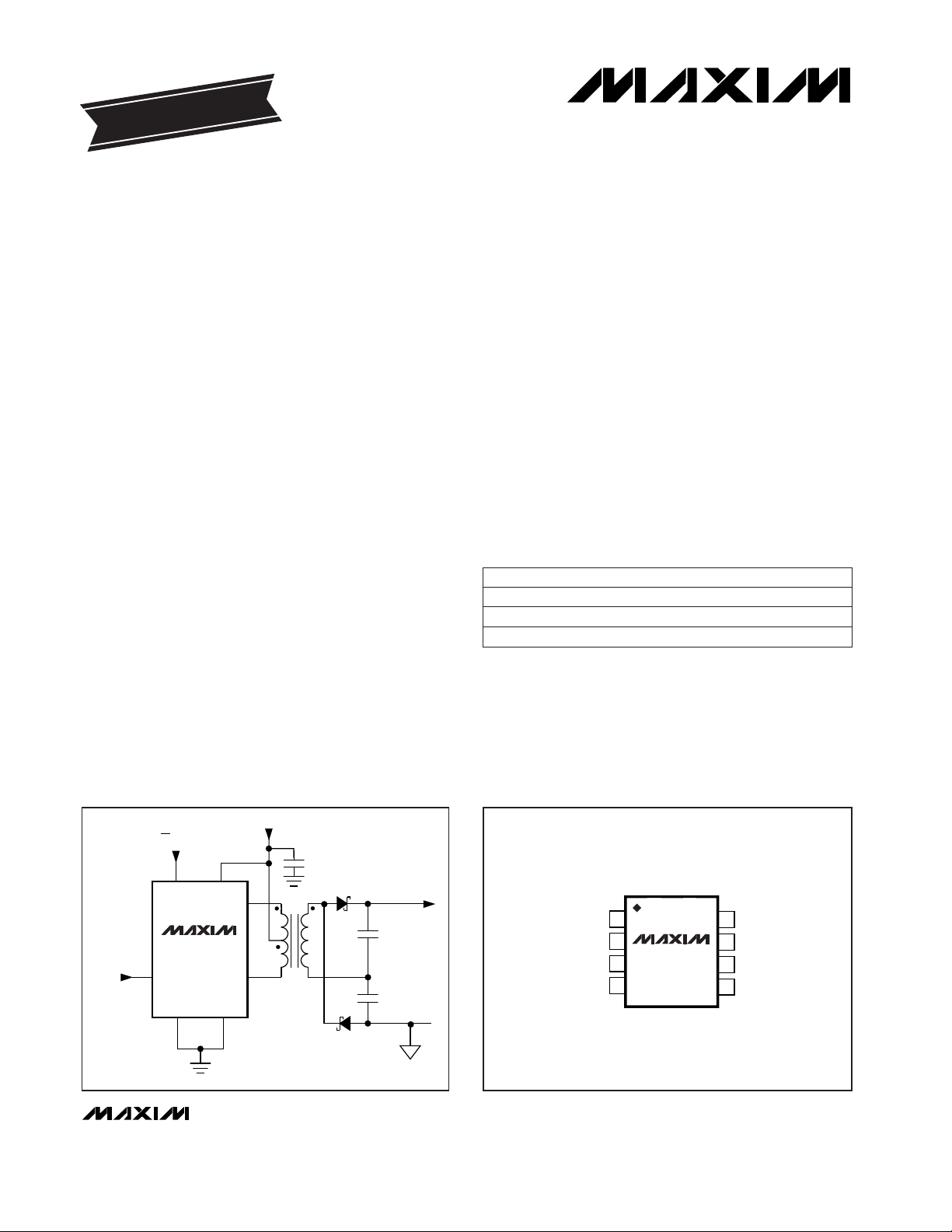
5V @ 150mA
OUTPUT
5V
ON / OFF
T1
CR2
CR1
__________Typical Operating Circuit
19-0372; Rev 4; 10/97
PART
MAX845C/D
MAX845EUA -40°C to +85°C
0°C to +70°C
TEMP. RANGE PIN-PACKAGE
Dice*
8 µMAX
EVALUATION KIT
AVAILABLE
*Contact factory for dice specifications.
_______________Ordering Information
MAX845ESA -40°C to +85°C 8 SO

MAX845
Isolated Transformer Driver
for PCMCIA Applications
2 _______________________________________________________________________________________
ABSOLUTE MAXIMUM RATINGS
ELECTRICAL CHARACTERISTICS
(VCC= 5V ±10%, TA= T
MIN
to T
MAX
, unless otherwise noted. Typical values are at TA= +25°C.)
Stresses beyond those listed under “Absolute Maximum Ratings” may cause permanent damage to the device. These are stress ratings only, and functional
operation of the device at these or any other conditions beyond those indicated in the operational sections of the specifications is not implied. Exposure to
absolute maximum rating conditions for extended periods may affect device reliability.
Note 1: Operating supply current is the current used by the MAX845 only. Load current is not included.
Note 2: Shutdown supply current includes output switch leakage currents.
Supply Voltage (V
CC
)...............................................-0.3V to +7V
Control Input Voltage (SD, FS)...................-0.3V to (V
CC
+ 0.3V)
Peak Output Switch Current (D1, D2)......................................1A
Output Switch Voltage (D1, D2).............................................12V
Average Output Switch Current (D1, D2) .........................200mA
Continuous Power Dissipation (T
A
= +70°C)
SO (derate 5.88mW/°C above +70°C).........................471mW
µMAX (derate 4.10mW/°C above +70°C) ....................330mW
Operating Temperature Range ...........................-40°C to +85°C
Storage Temperature Range.............................-65°C to +160°C
Junction Temperature......................................................+150°C
Lead Temperature (soldering, 10sec).............................+300°C
FS = V
CC
= 5.5V
FS = VCC= 4.5V
D1, D2; 100mA
Low
FS = V
CC
FS = 0V
High
SD = V
CC
FS = 0V, VCC= 4.5V
FS = 0V, VCC= 5.5V
Low
No load, SD = 0V, FS = V
CC
High
CONDITIONS
V2.5 2.2
µA
10
FS Input Current
50
V
0.8
FS Input Threshold
2.4
550 860 1100
450 675 900
Ω1.5 4.0Switch On-Resistance
pA10Shutdown Input Leakage Current
V
0.8
Shutdown Input Threshold
2.4
µA0.4Shutdown Supply Current (Note 2)
500
kHz
575
Switch Frequency
mA1.1 5.0Operating Supply Current (Note 1)
UNITSMIN TYP MAXPARAMETER
Minimum Start-Up Voltage

MAX845
Isolated Transformer Driver
for PCMCIA Applications
_______________________________________________________________________________________
3
40
-20 60
OUTPUT RESISTANCE vs. TEMPERATURE
30
MAX845-01
TEMPERATURE (°C)
OUTPUT RESISTANCE (Ω)
20 100
20
15
10
35
25
-40 0 8040
VIN = 4.5V
VIN = 5.5V
FIGURE 11c
7.5
2.5
-20 60
OUTPUT RESISTANCE vs. TEMPERATURE
3.5
6.0
MAX845-02
TEMPERATURE (°C)
OUTPUT RESISTANCE (Ω)
20 100
5.0
4.5
3.0
4.0
7.0
6.5
5.5
-40 0 8040
FIGURE 11b
1.6
1.4
1.2
0.2
-20 60
SHUTDOWN SUPPLY CURRENT
vs. TEMPERATURE
MAX845-03
TEMPERATURE (°C)
SHUTDOWN CURRENT (µA)
20 100
0.6
1.0
-40 0 8040
0.8
0.4
SD = V
CC
1000
950
600
-20 60
D1, D2 FREQUENCY vs. TEMPERATURE
MAX845-04
TEMPERATURE (°C)
FREQUENCY (kHz)
20 100
750
900
850
-40 0 8040
800
700
650
VIN = 5.5V
VIN = 4.5V
VIN = 5.0V
VIN = 6.0V
90
100
0
60
140 160
EFFICIENCY vs. LOAD CURRENT
20
70
MAX845-07
LOAD CURRENT (mA)
EFFICIENCY (%)
20 100
50
40
10
30
80
60
0
8040
120
FIGURE 11b
FIGURE 11c
850
800
500
550
-20 60
D1, D2 FREQUENCY vs. TEMPERATURE
MAX845-05
TEMPERATURE (°C)
FREQUENCY (kHz)
20 100
650
750
-40
0 8040
700
600
FS HIGH
VIN = 5.0V
FS LOW
1.5
1.4
0.8
-20 60
SUPPLY CURRENT vs. TEMPERATURE
MAX845-06
TEMPERATURE (°C)
SUPPLY CURRENT (mA)
20 100
1.0
-40 0 8040
0.9
1.1
1.3
1.2
1.7
1.6
VIN = 4.5V
VIN = 5.0V
VIN = 5.5V
VIN = 6.0V
7.5
2.5
0 40
OUTPUT VOLTAGE vs. LOAD CURRENT
3.5
6.5
MAX845-08
LOAD CURRENT (mA)
OUTPUT VOLTAGE (V)
80
5.5
4.5
3.0
4.0
7.0
6.0
5.0
20 60 140120100 160
TRANSFORMERS
USED IN FIGURE 11b
TGM-010P3
TGM-030P3
TGM-020P3
15
5
0 40
OUTPUT VOLTAGE vs. LOAD CURRENT
7
13
MAX845-09
LOAD CURRENT (mA)
OUTPUT VOLTAGE (V)
80
11
9
6
8
14
12
10
20 60 140120100 160
TRANSFORMERS
USED IN FIGURE 11c
TGM-010P3
TGM-030P3
TGM-020P3
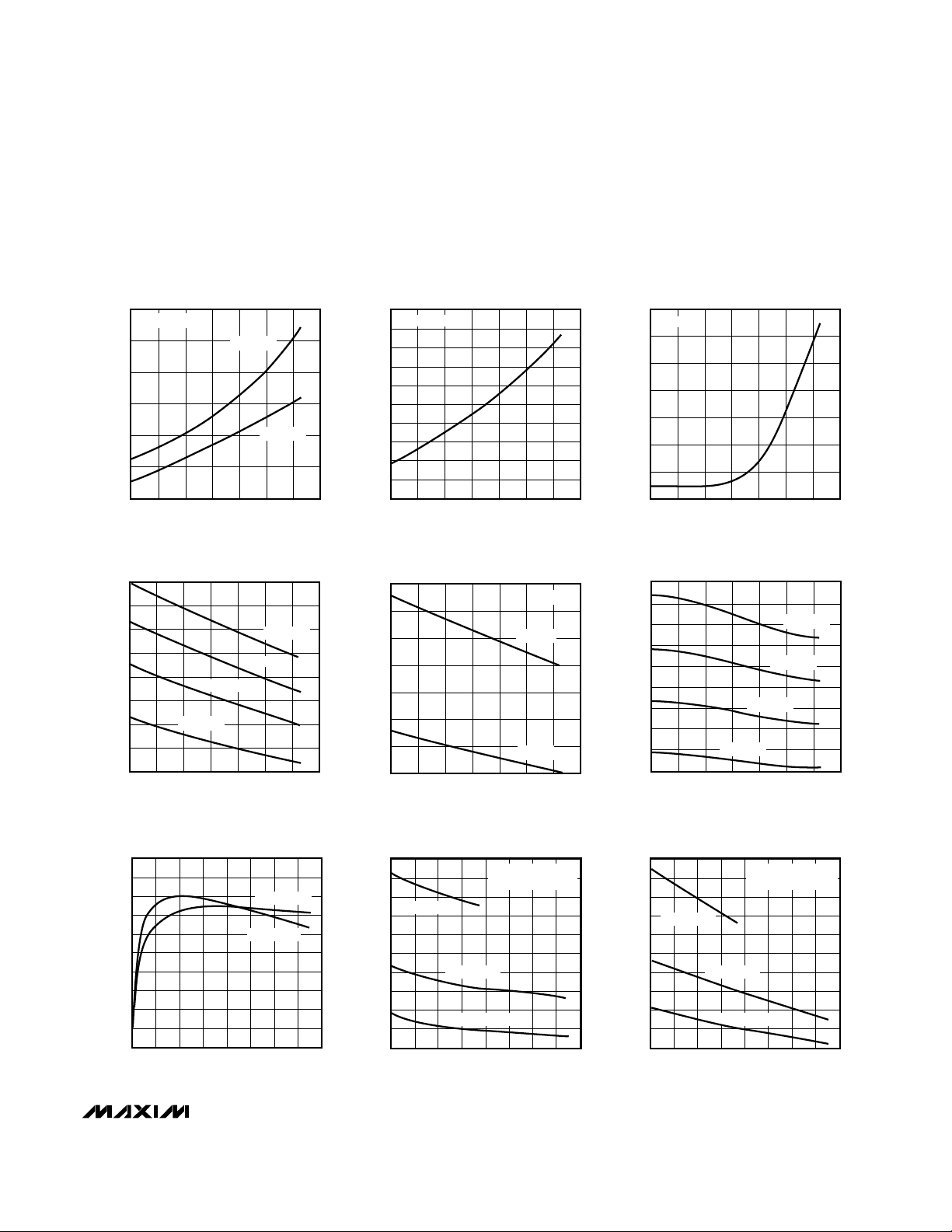
__________________________________________Typical Operating Characteristics
(
Typical Operating Circuit
, VIN= 5V, C1 = 0.1µF, C2 = C3 = 0.33µF, T1 = Halo TGM-010P3, CR1 = CR2 = MBR0520, FS = VCC,
T
A
= +25°C, unless otherwise noted.)

MAX845
Isolated Transformer Driver
for PCMCIA Applications
4 _______________________________________________________________________________________
____________________________Typical Operating Characteristics (continued)
(
Typical Operating Circuit
, VIN= 5V, C1 = 0.1µF, C2 = C3 = 0.33µF, T1 = Halo TGM-010P3, CR1 = CR2 = MBR0520, FS = VCC,
TA= +25°C, unless otherwise noted.)
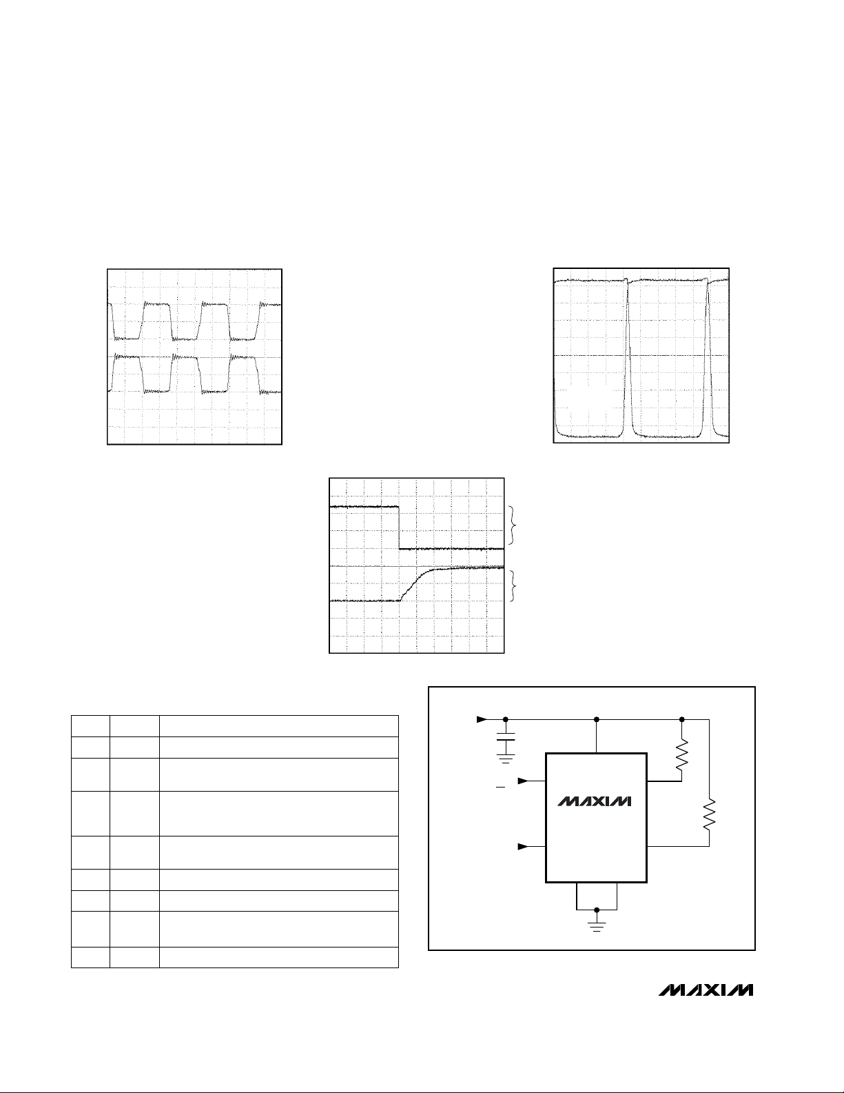
SWITCHING WAVEFORMS
(TWO CYCLES)
5V/div
400ns/div
D1
D2
SWITCHING WAVEFORM
(BREAK-BEFORE-MAKE)
500mV/div
200ns/div
D2OFFD1OFF
CIRCUIT
OF FIG. 1
D2ON D1ON
TIME FROM SHUTDOWN TO POWER-UP
2V/div
5µs/div
SD
OUTPUT
_____________________Pin Description
No Connect. Not internally connected.N.C.5
+5V Supply VoltageV
CC
6
Ground. Connect both GND1 and GND2 to
ground.
GND27
Open Drain of N-Channel Transformer Drive 2D28
Shutdown. Ground for normal operation,
connect to V
CC
for shutdown.
SD4
Frequency Select (internal pull-up). If FS =
VCCor open, switch frequency = 725kHz; if
FS = 0V, switch frequency = 535kHz.
FS3
PIN
Ground. Connect both GND1 and GND2 to
ground.
GND12
Open Drain of N-Channel Transformer Drive 1D11
FUNCTIONNAME
Figure 1. Test Circuit
V
IN
5V
ON / OFF
FREQUENCY
SELECT
C1
0.1µF
4
SD
3
6
V
CC
MAX845
GND1 GND2
2 7
R1
50Ω
1
D1
R2
50Ω
8
D2FS

_______________Detailed Description
The MAX845 is a transformer driver specifically
designed to provide isolated power for PCMCIA and
other height- and/or space-sensitive applications. It
drives a center-tapped transformer primary from a 5V
or 3.3V DC power supply. The secondary can be
wound to provide any isolated DC voltage needed at
power levels up to 750mW.
The 450kHz minimum switching frequency allows the
use of very thin transformers, making the MAX845 ideal
for PCMCIA and other space-limited applications. The
MAX845 is designed to drive a single transformer less
than 0.09 inches (2.3mm) in height, including package.
Further reduction down to 0.050 inches (1.27mm) can
be achieved using a transformer without a package.
The MAX845 consists of an RC oscillator driving a pair
of N-channel power switches. The oscillator runs at
double the output frequency, driving a toggle flip-flop
to ensure 50% duty cycle to each of the switches.
Internal circuitry ensures break-before-make action
between the two switches.
A low-current shutdown mode disables all internal circuitry, including the oscillator and both power switches.
Drive the shutdown pin (SD) high to shut down the part;
drive SD low for normal operation. The SD pin has no
internal default condition and must not be allowed to
float.
Most MAX845 applications will operate at high frequencies. The frequency-select pin (FS) is pulled high or left
open (FS is internally pulled up to VCC) to operate at a
minimum of 450kHz. Pulling FS low selects the low-frequency state.
Theory of Operation
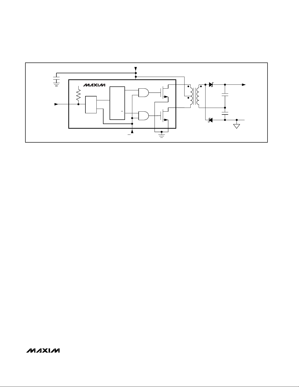
Figure 2 shows the MAX845 driving both a TGM-010P3
transformer with a center-tapped primary, and a secondary with a voltage-doubler rectifier topology. All of the
transformers driven by the MAX845 must have a center
tap with VINapplied. Whenever one of the MAX845 outputs (D1 or D2) goes low, the other goes to approximately double the supply voltage. A voltage is induced in the
secondary and the rectifier diodes steer the currents into
the appropriate output capacitor. On alternate half
cycles, each capacitor is charged. The output voltage is
the sum of the voltages from each output capacitor. This
topology yields the simplest and smallest transformer
because the least number of secondary turns is required
for a given voltage.
__________Applications Information
With the MAX845 transformer driver, designers have
the advantages of push/pull converter topology in
space-sensitive applications. The push/pull DC-DC
converter topology allows isolated multiple outputs,
step-up/step-down or inverted outputs, easier filtering
on the input and the output, and lower overall noise.
Isolated Power for PCMCIA Applications
Medical instrumentation, modems, and LAN-interface
cards often require isolated power supplies. One of the
best switching-regulator topologies for this application
is the push/pull forward-converting DC-DC power supply shown in Figures 3 and 4. Because the transformer
works in the forward mode (rather than the flyback
mode), its core does not store energy and, therefore,
can be small. Input and output capacitors can be small
because of the high-frequency and continuous-current
waveforms.
MAX845
Isolated Transformer Driver
for PCMCIA Applications
_______________________________________________________________________________________ 5
MAX845
D1
D2
FS
GND2 GND1
V
CC
FREQUENCY
SELECT
C2
C3
C1
OUTPUT
5V @ 150mA
5V
N
N
Q
Q
OSC
F / F
V
IN
SD
ON / OFF
400kHz/
700kHz
T
ISO
GND
V
CC
CR1
CR2
Figure 2. Detailed Block Diagram
 Loading...