

_______________General Description
The MAX823/MAX824/MAX825* microprocessor (µP)
supervisory circuits combine reset output, watchdog,
and manual-reset input functions in a 5-pin SOT23-5
package. They significantly improve system reliability
and accuracy compared to separate ICs or discrete
components. The MAX823/MAX824/MAX825 are
specifically designed to ignore fast transients on VCC.
Five preprogrammed reset threshold voltages are
available, designated by the following package
suffixes: L = 4.63V, M = 4.38V, T = 3.08V, S = 2.93V,
and R = 2.63V. All three devices have an active-low
reset output, which is guaranteed to be in the correct
state for VCCdown to 1V. The MAX824/MAX825 also
have an active-high reset output. The following
Selector
Guide
explains the functions offered in this series of
parts.
________________________Applications
Battery-Powered Computers and Controllers
Embedded Controllers
Intelligent Instruments
Automotive Systems
Critical µP Monitoring
Portable/Battery-Powered Equipment
____________________________Features
♦ Precision Monitoring of +3V, +3.3V, and +5V
Power Supplies
♦ Operating Current: 10µA (MAX823L/M)
3µA (MAX825T/S/R)
♦ Fully Specified Over Temperature
♦ 140ms Min Power-On Reset
♦ Guaranteed RESET Valid to V
CC
= 1V
♦ Power-Supply Transient Immunity
♦ Watchdog Timer with 1.6sec Timeout
(MAX823/MAX824)
♦ Manual-Reset Input (MAX823/MAX825)
♦ No External Components
MAX823/MAX824/MAX825
5-Pin Microprocessor Supervisory Circuits
________________________________________________________________
Maxim Integrated Products
1
1
5
2
3
4
1
5
2
3
4
1
5
2
3
4
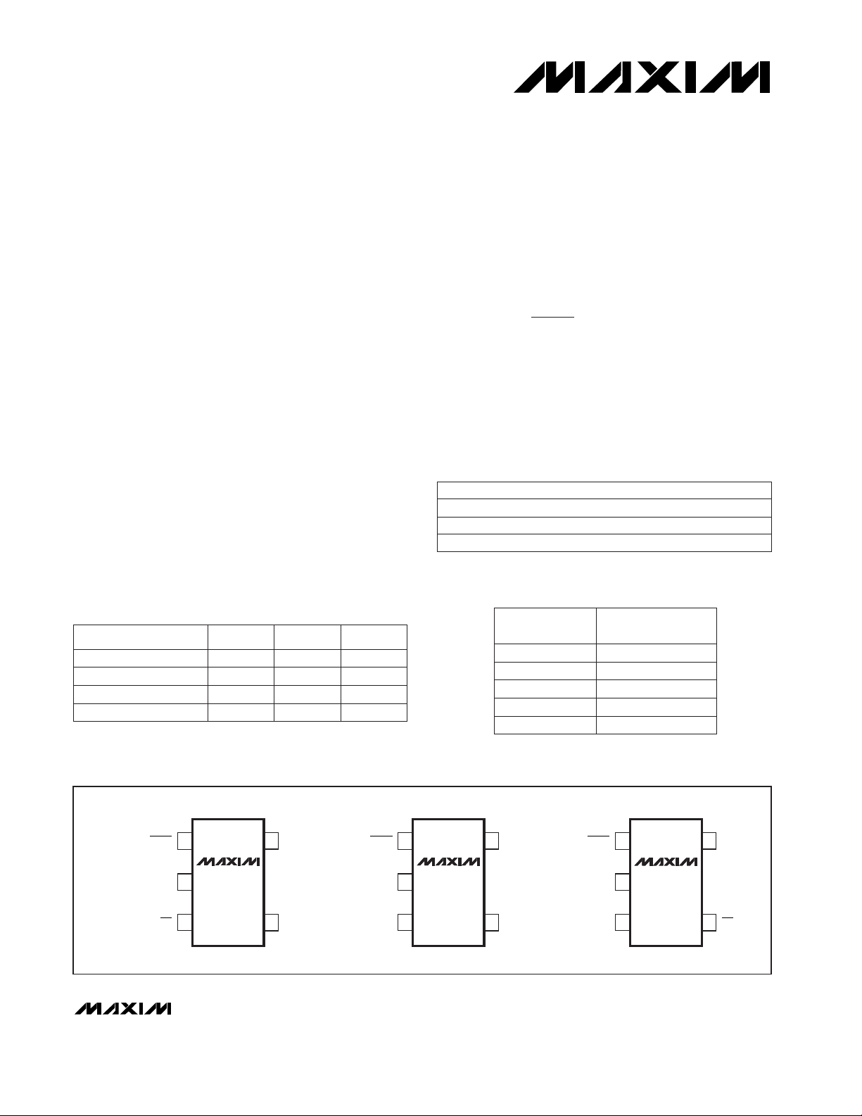
GND
WDI
MR
V
CC
RESET
MAX823
SOT23-5
TOP VIEW
GND
WDI
RESET
V
CC
RESET
MAX824
SOT23-5
GND
MR
RESET
V
CC
RESET
MAX825
SOT23-5
__________________________________________________________Pin Configurations
_____________________Selector Guide
19-0487; Rev 1; 6/97
PART
†
MAX823_EUK
MAX824_EUK -40°C to +85°C
-40°C to +85°C
TEMP. RANGE PIN-PACKAGE
5 SOT23-5
5 SOT23-5
______________Ordering Information
†
Insert the desired suffix letter (from the table below) into the
blank to complete the part number.
For free samples & the latest literature: http://www.maxim-ic.com, or phone 1-800-998-8800.
For small orders, phone 408-737-7600 ext. 3468.
MAX825_EUK -40°C to +85°C 5 SOT23-5
MAX823
Active-Low Reset
✔
Active-High Reset —
FUNCTION
Watchdog Input
✔
MAX824
✔
✔
✔
MAX825
✔
✔
—
Manual-Reset Input
✔
—
✔
SUFFIX
RESET
THRESHOLD (V)
L 4.63
M 4.38
T 3.08
S 2.93
R 2.63
Typical Operating Circuit appears at end of data sheet.
Marking Information appears at end of data sheet.
*Patents Pending
MAX823/MAX824/MAX825
5-Pin Microprocessor Supervisory Circuits
2 _______________________________________________________________________________________
ABSOLUTE MAXIMUM RATINGS
ELECTRICAL CHARACTERISTICS
(VCC= +4.75V to +5.5V for MAX82_L, VCC= +4.5V to +5.5V for MAX82_M, VCC= +3.15V to +3.6V for MAX82_T, VCC= +3V
to +3.6V for MAX82_S, VCC= +2.7V to +3.6V for MAX82_R, TA= T
MIN
to T
MAX
, unless otherwise noted. Typical values are at
TA= +25°C.) (Note 1)
Stresses beyond those listed under “Absolute Maximum Ratings” may cause permanent damage to the device. These are stress ratings only, and functional
operation of the device at these or any other conditions beyond those indicated in the operational sections of the specifications is not implied. Exposure to
absolute maximum rating conditions for extended periods may affect device reliability.
VCC........................................................................-0.3V to +6.0V
All Other Pins..............................................-0.3V to (V
CC
+ 0.3V)
Input Current, All Pins Except RESET and
RESET..............20mA
Output Current, RESET, RESET ..........................................20mA
Rate of Rise, V
CC
............................................................100V/µs
Continuous Power Dissipation (T
A
= +70°C)
SOT23-5 (derate 7.1mW/°C above +70°C)...................571mW
Operating Temperature Range
MAX82_EUK .....................................................-40°C to +85°C
Storage Temperature Range.............................-65°C to +160°C
Lead Temperature (soldering, 10sec).............................+300°C
MAX82_M
TA= +25°C
TA= -40°C to +85°C
WDI and MR
unconnected
4.25 4.50
TA= -40°C to +85°C
TA= 0°C to +70°C
4.31 4.38 4.45
MAX82_T/S/R
MAX82_L/M
MAX82_L
TA= +25°C
TA= -40°C to +85°C
MR unconnected
MAX82_S
CONDITIONS
TA= +25°C
TA= -40°C to +85°C 2.85 3.00
2.89 2.93 2.96
MAX82_T
TA= +25°C
TA= -40°C to +85°C 3.00 3.15
3.04 3.08 3.11
MAX82_L/M
MAX82_T/S/R
mV
5
Reset Threshold Hysteresis
10
MAX82_R
TA= +25°C
TA= -40°C to +85°CV2.55 2.70
V
RST
Reset Threshold
2.59 2.63 2.66
MAX823T/S/R,
MAX824T/S/R
5 12
V
1.2
V
CC
1.0 5.5
MAX823L/M,
MAX824L/M
MAX825L/M
Operating Voltage Range
ms
140 200 280
t
RP
Reset Timeout Period
140 200 280
ppm/°C40
Reset Threshold Temperature
Coefficient
4.50 4.75
10 24
4.5 12
µA
3 8
I
SUPPLY
Supply Current
4.56 4.63 4.70
UNITSMIN TYP MAXSYMBOLPARAMETER
MAX825T/S/R
ELECTRICAL CHARACTERISTICS (continued)
(VCC= +4.75V to +5.5V for MAX82_L, VCC= +4.5V to +5.5V for MAX82_M, VCC= +3.15V to +3.6V for MAX82_T, VCC= +3V
to +3.6V for MAX82_S, V
CC
= +2.7V to +3.6V for MAX82_R, TA= T
MIN
to T
MAX
, unless otherwise noted. Typical values are at
T
A
= +25°C.) (Note 1)
Note 1: Over-temperature limits are guaranteed by design and not production tested.
Note 2: The RESET short-circuit current is the maximum pull-up current when RESET is driven low by a µP bidirectional reset pin.
Note 3: WDI is internally serviced within the watchdog period if WDI is left unconnected.
Note 4: The WDI input current is specified as the average input current when the WDI input is driven high or low. The WDI input is
designed to drive a three-stated-output device with a 10µA maximum leakage current and a maximum capacitive load of
200pF. This output device must be able to source and sink at least 200µA when active.
MAX823/MAX824/MAX825
5-Pin Microprocessor Supervisory Circuits
_______________________________________________________________________________________ 3
V
RST
- VCC= 100mV
MAX824T/S/R, MAX825T/S/R,
VCC= V
RST
max, I
SINK
= 1.2mA
MAX82_L/M, VCC= V
RST
max,
I
SOURCE
= 120µA
MAX824L/M, MAX825L/M,
VCC= V
RST
max, I
SINK
= 3.2mA
VCC> 1.8V, I
SOURCE
= 150µA
MAX82_L/M, RESET = 0V, VCC= 5.5V
CONDITIONS
µs20
VCCto RESET Delay
V
0.3
V
OL
RESET Output Voltage
VCC- 1.5
0.4
0.8V
CC
V
OH
800
UNITSMIN TYP MAXSYMBOLPARAMETER
MAX82_T/S/R, VCC= V
RST
max,
I
SOURCE
= 30µA
0.8V
CC
V
OH
MAX82_T/S/R, VCC= V
RST
min,
I
SINK
= 1.2mA
MAX82_L/M, VCC= V
RST
min,
I
SINK
= 3.2mA
0.3
0.4
TA= -40°C to +85°C, VCC= 1.2V,
VCCfalling, V
BATT
= 0V, I
SINK
= 100µA
TA= 0°C to +70°C, VCC= 1V,
VCCfalling, I
SINK
= 50µA
V
0.3
V
OL
RESET Output Voltage
0.3
MAX82_T/S/R, RESET = 0V, VCC= 3.6V
µA
400
I
SOURCE
RESET Output Short-Circuit
Current (Note 2)
VIL= 0.4V, VIH= 0.8V
CC
ns50t
WDI
WDI Pulse Width
sec1.12 1.60 2.40t
WD
Watchdog Timeout Period
WDI = 0V, time average
WDI = VCC, time average
VCC= 5V
µA
-20 -15
WDI Input Current (Note 4)
120 160
V
0.7V
CC
V
IH
WDI Input Threshold (Note 3)
0.3V
CC
V
IL
µs1.0
MR Pulse Width
V
0.7V
CC
V
IH
MR Input Threshold
0.3V
CC
V
IL
kΩ35 52 75
MR Pull-Up Resistance (internal)
ns500
MR to Reset Delay
ns100
MR Noise Immunity (pulse width
with no reset)
MANUAL-RESET INPUT (MAX823/MAX825)
WATCHDOG INPUT (MAX823/MAX824)

MAX823/MAX824/MAX825
5-Pin Microprocessor Supervisory Circuits
4 _______________________________________________________________________________________
__________________________________________Typical Operating Characteristics
(MAX823L, VCC= +5V, TA= +25°C, unless otherwise noted.)
12.5
7.5
-40 -20 40 100
VCC SUPPLY CURRENT
vs. TEMPERATURE
8.5
8.0
9.0
11.5
12.0
MAX823/4/5-01
TEMPERATURE (°C)
SUPPLY CURRENT (µA)
0 20 8060
10.5
11.0
9.5
10.0
250
150
-40 -20 40 100
RESET TIMEOUT PERIOD
vs. TEMPERATURE
170
160
180
230
240
MAX823/4/5-02
TEMPERATURE (°C)
RESET TIMEOUT PERIOD (ms)
0 20 8060
210
220
190
200
30
0
-40 -20 40 100
RESET COMPARATOR PROPAGATION DELAY
vs. TEMPERATURE
5
25
MAX823/4/5-03
TEMPERATURE (°C)
PROPAGATION DELAY (µs)
0 20 8060
20
10
15
VCC FALLING
2.0
1.0
-40 -20 40 100
WATCHDOG TIMEOUT PERIOD
vs. TEMPERATURE
1.2
1.1
1.3
1.8
1.9
MAX823/4/5-04
TEMPERATURE (°C)
WATCHDOG TIMEOUT PERIOD (sec)
0 20 8060
1.6
1.7
1.4
1.5
1.06
0.94
0.96
0.98
1.00
1.02
1.04
-40 -20 40 100
NORMALIZED RESET THRESHOLD
VOLTAGE vs. TEMPERATURE
MAX823/4/5-05
TEMPERATURE (°C)
NORMALIZED RESET THRESHOLD (V)
0 20 8060
0
20
40
60
80
100
120
140
160
40 100 200180120 140 160
MAXIMUM VCC TRANSIENT DURATION
vs. RESET THRESHOLD OVERDRIVE
MAX823/4/5-06
RESET THRESHOLD OVERDRIVE (mV), V
RST
- V
CC
TRANSIENT DURATION (µs)
0 20 8060
RESET OCCURS
ABOVE CURVE

MAX823/MAX824/MAX825
5-Pin Microprocessor Supervisory Circuits
_______________________________________________________________________________________ 5
______________________________________________________________Pin Description
MAX823
MAX824
MAX825
V
CC
V
CC
WDI
(MAX823/MAX824
ONLY)
1.25V
GND
RESET
(MAX824/MAX825
ONLY)
RESET
MR
(MAX823/MAX825
ONLY)
RESET
GENERATOR
WATCHDOG
TIMER
WATCHDOG
TRANSITION
DETECTOR
FUNCTION
1 1
Active-Low Reset Output. Pulses low for 200ms when triggered, and remains
low whenever V
CC
is below the reset threshold or when MR is a logic low. It
remains low for 200ms after one of the following occurs: V
CC
rises above the
reset threshold, the watchdog triggers a reset, or MR goes low to high.
2 2 Ground. 0V reference for all signals.
3 —
Manual-Reset Input. A logic low on MR asserts reset. Reset remains asserted as
long as MR is held low and for 200ms after MR returns high. The active-low input
has an internal 52kΩ pull-up resistor. It can be driven from a CMOS-logic line or
shorted to ground with a switch. Leave open or connect to V
CC
if unused.
— 3
Active-High Reset Output. Inverse of RESET.
5 5 Supply Voltage
4 4
Watchdog Input. If WDI remains either high or low for longer than the watchdog timeout period, the internal watchdog timer runs out and a reset is triggered. The internal watchdog timer clears whenever reset is asserted, or
whenever WDI sees a rising or falling edge. If WDI is left unconnected or is
connected to a three-stated buffer output, the watchdog feature is disabled.
NAME
1
RESET
2 GND
4
MR
3 RESET
5 V
CC
— WDI
Figure 1. Functional Diagram
MAX824MAX823 MAX825
PIN

MAX823/MAX824/MAX825
5-Pin Microprocessor Supervisory Circuits
6 _______________________________________________________________________________________
_______________Detailed Description
RESET Output
A microprocessor’s (µP’s) reset input starts the µP in a
known state. The MAX823/MAX824/MAX825 µP supervisory circuits assert a reset to prevent code-execution
errors during power-up, power-down, and brownout
conditions. RESET is guaranteed to be a logic low for
VCCdown to 1V. Once VCCexceeds the reset threshold, an internal timer keeps RESET low for the specified
reset timeout period (tRP); after this interval, RESET
returns high (Figure 2).
If a brownout condition occurs (VCCdips below the
reset threshold), RESET goes low. Each time RESET is
asserted it stays low for the reset timeout period. Any
time VCCgoes below the reset threshold the internal
timer restarts. RESET both sources and sinks current.
RESET on the MAX824/MAX825 is the inverse of
RESET.
Manual-Reset Input (MAX823/MAX825)
Many µP-based products require manual-reset capability, allowing the operator, a test technician, or external
logic circuitry to initiate a reset. On the MAX823/
MAX825, a logic low on MR asserts reset. Reset remains
asserted while MR is low, and for tRP(200ms nominal)
after it returns high. MR has an internal 52kΩ pull-up
resistor, so it can be left open if not used. This input can
be driven with CMOS-logic levels or with open-drain/
collector outputs. Connect a normally open momentary
switch from MR to GND to create a manual-reset function; external debounce circuitry is not required. If MR is
driven from long cables or the device is used in a noisy
environment, connect a 0.1µF capacitor from MR to
GND to provide additional noise immunity.
Watchdog Input (MAX823/MAX824)
In the MAX823/MAX824, the watchdog circuit monitors
the µP’s activity. If the µP does not toggle the watchdog
input (WDI) within tWD(1.6sec), reset asserts. The internal 1.6sec timer is cleared by either a reset pulse or by
toggling WDI, which detects pulses as short as 50ns.
While reset is asserted, the timer remains cleared and
does not count. As soon as reset is released, the timer
starts counting (Figure 3).
Disable the watchdog function by leaving WDI unconnected or by three-stating the driver connected to WDI.
The watchdog input is internally driven low during the
first 7/8 of the watchdog timeout period and high for the
last 1/8 of the watchdog timeout period. When WDI is
left unconnected, this internal driver clears the 1.6sec
timer every 1.4sec. When WDI is three-stated or unconnected, the maximum allowable leakage current is
10µA and the maximum allowable load capacitance is
200pF.
__________Applications Information
Watchdog Input Current
The MAX823/MAX824 WDI inputs are internally driven
through a buffer and series resistor from the watchdog
counter (Figure 1). When WDI is left unconnected, the
watchdog timer is serviced within the watchdog timeout
period by a low-high-low pulse from the counter chain.
For minimum watchdog input current (minimum overall
power consumption), leave WDI low for the majority of
the watchdog timeout period, pulsing it low-high-low
once within the first 7/8 of the watchdog timeout period
to reset the watchdog timer. If WDI is externally driven
high for the majority of the timeout period, up to 160µA
can flow into WDI.
V
CC
1V
1V
t
RD
V
RST
V
RST
t
RD
RESET
GND
RESET
t
RP
t
RP
Figure 2. Reset Timing Diagram
V
CC
t
WD
t
RP
t
RP
t
RST
WDI
RESET*
*RESET ON THE MAX824/MAX825 IS THE INVERSE OF RESET.
Figure 3. MAX823/MAX824 Watchdog Timing Relationship

Interfacing to µPs with
Bidirectional Reset Pins
The RESET output maximum pull-up current is 800µA
for L/M versions (400µA for T/S/R versions). This allows
µPs with bidirectional resets, such as the 68HC11, to
force RESET low when the MAX823/MAX824/MAX825
are pulling RESET high (Figure 4).
Negative-Going VCCTransients
These supervisors are relatively immune to shortduration, negative-going VCCtransients (glitches), which
usually do not require the entire system to shut down.
Resets are issued to the µP during power-up, powerdown, and brownout conditions.
The
Typical Operating Characteristics
show a graph of
the MAX823L’s Maximum VCCTransient Duration vs.
Reset Threshold Overdrive, for which reset pulses are
not generated. The graph was produced using nega tive-going VCCpulses, starting at 5V and ending below
the reset threshold by the magnitude indicated (reset
threshold overdrive). The graph shows the maximum
pulse width that a negative-going VCCtransient can
typically have without triggering a reset pulse. As the
amplitude of the transient increases (i.e., goes farther
below the reset threshold), the maximum allowable
pulse width decreases. Typically, a VCCtransient that
goes 100mV below the reset threshold and lasts for
15µs or less will not trigger a reset pulse.
An optional 0.1µF bypass capacitor mounted close to
V
CC
provides additional transient immunity.
Watchdog Software Considerations
(MAX823/MAX824)
One way to help the watchdog timer monitor software
execution more closely is to set and reset the watchdog
input at different points in the program, rather than
pulsing the watchdog input high-low-high or low-highlow. This technique avoids a stuck loop, in which the
watchdog timer would continue to be reset inside the
loop, keeping the watchdog from timing out.
Figure 5 shows an example of a flow diagram where the
I/O driving the watchdog input is set high at the beginning of the program, set low at the beginning of every
subroutine or loop, then set high again when the program returns to the beginning. If the program should
hang in any subroutine, the problem would quickly be
corrected, since the I/O is continually set low and the
watchdog timer is allowed to time out, causing a reset
or interrupt to be issued. As described in the
Watchdog
Input Current
section, this scheme results in higher time
average WDI input current than does leaving WDI low
for the majority of the timeout period and periodically
pulsing it low-high-low.
MAX823/MAX824/MAX825
5-Pin Microprocessor Supervisory Circuits
_______________________________________________________________________________________ 7
MAX823
MAX824
MAX825
µP
V
CC
V
CC
V
CC
GND
GND
RESET
I
SOURCE
MAX = 800µA L, M
400µA T, S, R
RESET
GENERATOR
Figure 4. Interfacing to µPs with Bidirectional Resets
START
SET WDI
HIGH
PROGRAM
CODE
SUBROUTINE OR
PROGRAM LOOP
SET WDI LOW
RETURN
Figure 5. Watchdog Flow Diagram

MAX823/MAX824/MAX825
5-Pin Microprocessor Supervisory Circuits
Maxim cannot assume responsibility for use of any circuitry other than circuitry entirely embodied in a Maxim product. No circuit patent licenses are
implied. Maxim reserves the right to change the circuitry and specifications without notice at any time.
8
____________________Maxim Integrated Products, 120 San Gabriel Drive, Sunnyvale, CA 94086 408-377-7600
© 1997 Maxim Integrated Products Printed USA is a registered trademark of Maxim Integrated Products.
__________Typical Operating Circuit ___________________Chip Information
______________Package Information
TRANSISTOR COUNT: 607
MAX823
µP
V
CC
V
CC
V
CC
GND
MANUAL
RESET
RESET
I/O
RESET
MR
WDI
MARKING INFORMATION (TOP)
AAAI = MAX823L
AAAJ = MAX823M
AAAK = MAX823T
AAAL = MAX823S
AAAM = MAX823R
AAAN = MAX824L
AAAO = MAX824M
AAAP = MAX824T
AAAQ = MAX824S
AAAR = MAX824R
AAAS = MAX825L
AAAT = MAX825M
AAAU = MAX825T
AAAV = MAX825S
AAAW = MAX825R
XXXX
SOT5L.EPS
 Loading...