

Datasheet MAX822SUS-T, MAX822TUS-T, MAX821LUS-T, MAX821MUS-T, MAX822LUS-T Datasheet (Maxim)
...
General Description
The MAX821/MAX822 microprocessor (µP) supervisory
circuits monitor power supplies in µP and digital systems. They provide excellent circuit reliability and low
cost by eliminating external components and adjustments when used with 5V-powered or 3V-powered circuits. The MAX821/MAX822 also provide a power-on
reset timeout delay that is pin selectable to 1ms (max),
20ms (min), or 100ms (min).
These devices perform a single function: they assert a
reset signal whenever the VCCsupply voltage falls
below a preset threshold, and they keep reset asserted
for the pin-selected reset timeout delay after VCChas
risen above the reset threshold. The only difference
between the two devices is that the MAX821 has an
active-low RESET output (which is guaranteed to be in
the correct state for VCCdown to 1V), while the
MAX822 has an active-high RESET output. The reset
comparator is designed to ignore fast transients on
VCC. Reset thresholds suitable for operation with a variety of supply voltages are available.
Low supply current makes the MAX821/MAX822 ideal
for use in portable equipment. These devices come in a
4-pin SOT143 package.
________________________Applications
Bar-Code Scanners
Computers
Controllers
Intelligent Instruments
Critical µP and µC Power Monitoring
Portable/Battery-Powered Equipment
Features
♦ Pin-Selectable, Precision Power-On Reset Delay:
1ms (max), 20ms (min), or 100ms (min)
♦ Precision Monitoring of +3V to +5V Power-Supply
Voltages
♦ 2.5µA Supply Current
♦ Guaranteed Over Temperature (-40°C to +125°C)
♦ Guaranteed RESET Valid to VCC= 1V (MAX821)
♦ Power-Supply Transient Immunity
♦ No External Components
♦ SOT143 Package
MAX821/MAX822
4-Pin µP Voltage Monitors with Pin-Selectable
Power-On Reset Timeout Delay
________________________________________________________________ Maxim Integrated Products 1
1
2
4
3
V
CC
SRT
(RESET) RESET
GND
MAX821
MAX822
SOT143
TOP VIEW
( ) ARE FOR MAX822
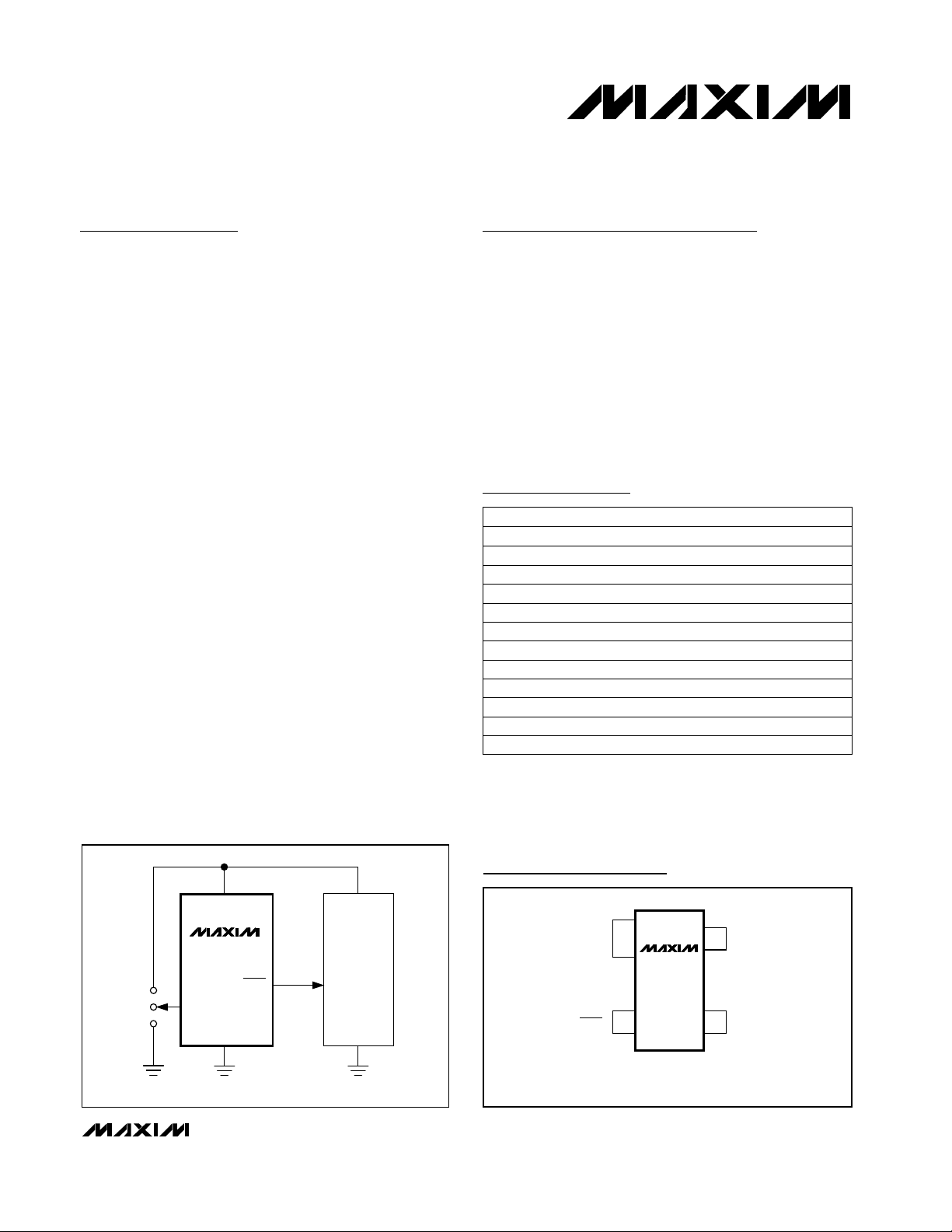
Pin Configuration
MAX821
MAX822
V
CC
RESET
(RESET)
RESET
INPUT
GND
V
CC
GND
µP
( ) ARE FOR MAX822
SRT
20ms
100ms
1ms
__________Typical Operating Circuit
19-1122; Rev 1; 12/99
PART
MAX821LUS-T
MAX821MUS-T 4.38
4.63
NOMINAL VTH(V) TOP MARK*
AZ_ _
BA_ _
Ordering Information
* The first two letters in the package top mark identify the part,
while the remaining two letters are the lot-tracking code.
For free samples & the latest literature: http://www.maxim-ic.com, or phone 1-800-998-8800.
For small orders, phone 1-800-835-8769.
MAX821PUS-T 4.00 BM_ _
MAX821TUS-T 3.08 BB_ _
MAX821SUS-T 2.93 BC_ _
MAX821UUS-T 2.78 BL_ _
MAX821RUS-T 2.63 BD_ _
MAX822LUS-T
4.63 BF_ _
MAX822MUS-T 4.38 BG_ _
MAX822TUS-T 3.08 BH_ _
MAX822SUS-T 2.93 BJ_ _
MAX822RUS-T 2.63 BK_ _
Note: These parts are offered in the SOT143-4 package, in the
extended temperature range (-40°C to +85°C).
MAX821/MAX822
4-Pin µP Voltage Monitors with Pin-Selectable
Power-On Reset Timeout Delay
2 _______________________________________________________________________________________
ABSOLUTE MAXIMUM RATINGS
ELECTRICAL CHARACTERISTICS
(VCC= full range, TA= -40°C to +125°C, unless otherwise noted. Typical values are at TA= +25°C.)
Stresses beyond those listed under “Absolute Maximum Ratings” may cause permanent damage to the device. These are stress ratings only, and functional
operation of the device at these or any other conditions beyond those indicated in the operational sections of the specifications is not implied. Exposure to
absolute maximum rating conditions for extended periods may affect device reliability.
Terminal Voltage (with respect to GND)
V
CC
......................................................................-0.3V to 6.0V
All Other Inputs.......................................-0.3V to (V
CC
+ 0.3V)
Input Current, V
CC
, SRT......................................................20mA
Output Current, RESET or RESET .......................................20mA
Continuous Power Dissipation (T
A
= +70°C)
SOT143-4 (derate 4mW/°C above +70°C)...................320mW
Operating Temperature Range .........................-40°C to +125°C
Storage Temperature Range.............................-65°C to +160°C
Lead Temperature (soldering, 10sec).............................+300°C
SRT = unconnected
V
0.5V
CC
V
OPEN
SRT Input Threshold
0.9V
CC
V
IH
0.07V
CC
V
IL
ms
100 160 200
t
RP
Reset Active Timeout Period 20 32 40
2.5 7.0
V
1.2 5.5
1.0 5.5
VCCRange
0.5 0.8 1
µs50VCCto Reset Delay (Note 1)
ppm/°C30Reset Threshold Tempco
V
2.55 2.70
V
TH
Reset Threshold (Note 1)
12
1.8 5.5
µA
9
I
CC
Supply Current
2.59 2.63 2.66
UNITSMIN TYP MAXSYMBOLPARAMETER
TA= -40°C to +85°C
TA= 0°C to +70°C
VCCfalling at 1mV/µs
RESET = low for MAX821,
RESET = high for MAX822
MAX82_R
MAX82_L/M/P,
VCC= 5.5V, I
OUT
= 0
MAX82_R/S/T/U,
V
CC
= 5.5V, I
OUT
= 0
CONDITIONS
4.56 4.63 4.70
4.50 4.75
4.31 4.38 4.45
4.25 4.50
MAX82_L
MAX82_M
3.97 4.00 4.04
3.91 4.09
2.89 2.93 2.96
3.04 3.08 3.11
2.85 3.00
3.00 3.15
MAX82_P
2.74 2.78 2.81
2.70 2.85
MAX82_S
MAX82_U
µA
-1 1
SRT Input Current (Note 2) 100
-100
RESET = low for MAX821,
RESET = high for MAX822
SRT = GND
SRT = V
CC
TA= +25°C
TA= +25°C
TA= +25°C
TA= +25°C
TA= +25°C
MAX82_T
TA= +25°C
TA= +25°C
TA= +25°C
TA= +25°C
SRT = GND
SRT = unconnected
SRT = V
CC
TA= -40°C to +125°C
TA= -40°C to +125°C
TA= -40°C to +125°C
TA= -40°C to +125°C
TA= -40°C to +125°C
TA= -40°C to +125°C
TA= -40°C to +125°C
TA= T
MIN
to T
MAX
TA= T
MIN
to T
MAX
MAX821/MAX822
4-Pin µP Voltage Monitors with Pin-Selectable
Power-On Reset Timeout Delay
_______________________________________________________________________________________ 3
Note 1: RESET output for MAX821; RESET output for MAX822.
Note 2: During reset active timeout period only.
Note 3: Guaranteed by design.
ELECTRICAL CHARACTERISTICS (continued)
(VCC= full range, TA= -40°C to +125°C, unless otherwise noted. Typical values are at TA= +25°C.)
0.3
0.4
pF20
SRT Input Capacitance
(Note 3) (see Setting
the Reset Timeout Delay
section)
UNITSMIN TYP MAXSYMBOLPARAMETER
MAX821R/S/T/U only, I
SINK
= 1.2mA,
VCC= V
TH(MIN)
MAX821L/M/P only, I
SINK
= 3.2mA,
VCC= V
TH(MIN)
Internal
CONDITIONS
0.3
V
OL
0.3
I
SINK
= 50µA
0.3
0.4
MAX822R/S/T only, I
SINK
= 1.2mA,
V
CC
= V
TH(MAX)
MAX822L/M only, I
SINK
= 3.2mA,
V
CC
= VTH(MAX)
V
0.8V
CC
V
OH
RESET Output Voltage
(MAX821)
VCC-1.5
MAX821R/S/T/U only, I
SOURCE
= 500µA,
VCC≥ V
TH(MAX)
MAX821L/M/P only, I
SOURCE
= 800µA,
VCC≥ V
TH(MAX)
0.6
-40
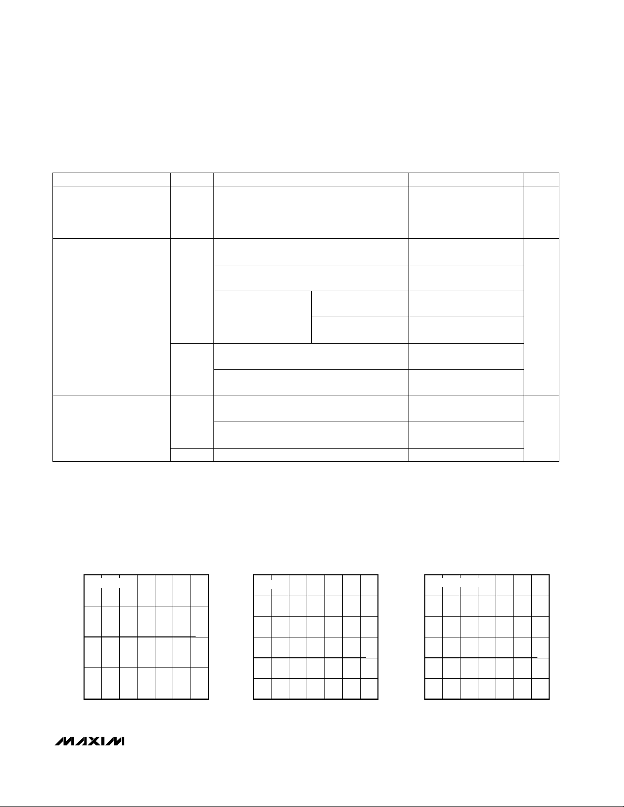
RESET TIMEOUT PERIOD
vs. TEMPERATURE
0.7
MAX 821/822 TOC-04
TEMPERATURE (°C)
RESET TIMEOUT PERIOD (ms)
40 60 80
0.9
0.8
-20 20 100
1.0
0
SRT = GND
30
-40
RESET TIMEOUT PERIOD
vs. TEMPERATURE
32
31
MAX 821/822 TOC-05
TEMPERATURE (°C)
RESET TIMEOUT PERIOD (ms)
40 60 80
35
34
33
-20 20 100
36
0
SRT = V
CC
150
-40
RESET TIMEOUT PERIOD
vs. TEMPERATURE
160
155
MAX 821/822 TOC-06
TEMPERATURE (°C)
RESET TIMEOUT PERIOD (ms)
40 60 80
175
170
165
-20 20 100
180
0
SRT = UNCONNECTED
V
OL
V
V
OH
RESET Output Voltage
(MAX822)
0.8V
CC
I
SOURCE
= 150µA, 1.4V ≤ VCC≤ V
TH(MIN)
__________________________________________Typical Operating Characteristics
(TA = +25°C, unless otherwise noted.)
TA= 0°C to +70°C,
VCC≥ 1V
TA = -40°C to +85°C,
VCC≥ 1.2V

MAX821/MAX822
4-Pin µP Voltage Monitors with Pin-Selectable
Power-On Reset Timeout Delay
4 _______________________________________________________________________________________
____________________________Typical Operating Characteristics (continued)
(TA = +25°C, unless otherwise noted.)
0.997
-40
NORMALIZED RESET THRESHOLD
vs. TEMPERATURE
0.999
0.998
MAX 821/822 TOC-07
TEMPERATURE (°C)
NORMALIZED RESET THRESHOLD (V)
40 60 80
1.002
1.001
1.000
-20 20 100
1.003
0
______________________________________________________________Pin Description
1
GND Ground
2
RESET
Active-Low Reset Output. RESET is low while VCCis below the reset threshold. It remains
low for the reset timeout period after the reset condition is terminated. The reset timeout
period is determined by the SRT input.
–
RESET
Active-High Reset Output. RESET is high while VCCis below the reset threshold. It remains
high for the reset timeout period after the reset condition is terminated. The reset timeout
period is determined by the SRT input.
3 SRT
Set Reset Timeout Input. Connect to GND for 1ms (max) delay; connect to VCCfor 20ms
(min) delay; leave unconnected for 100ms (min) delay.
4 V
CC
Supply Voltage
1
–
PIN
2
3
4
NAME FUNCTION
MAX821 MAX822
MAX82_R/S/T POWER-DOWN RESET DELAY
vs. TEMPERATURE
45
40
35
30
25
20
15
10
POWER-DOWN RESET DELAY (µs)
5
0
-40
VCC FALLING AT 1mV/µs
VCC FALLING AT 10mV/µs
-20 20 100
0
TEMPERATURE (°C)
NORMALIZED SUPPLY
CURRENT vs. TEMPERATURE
1.10
1.05
1.00
40 60 80
MAX 821/822 TOC-02
MAX 821/822 TOC-01
MAX82_L/M POWER-DOWN RESET DELAY
vs. TEMPERATURE
60
50
40
30
20
10
POWER-DOWN RESET DELAY (µs)
0
-40
FALLING AT 1mV/µs
V
CC
FALLING AT 10mV/µs
V
CC
-20 20 100
0
TEMPERATURE (°C)
40 60 80
MAX 821/822 TOC-03
0.95
NORMALIZED SUPPLY CURRENT (µA)
0.90
-40
-20 20 100
0
TEMPERATURE (°C)
40 60 80

_______________Detailed Description
Reset Output
A microprocessor’s (µP’s) reset input starts the µP in a
known state. These µP supervisory circuits assert reset
to prevent code-execution errors during power-up,
power-down, or brownout conditions. They also provide
a reset timeout delay that is pin programmable to 1ms
(max), 20ms (min), or 100ms (min). This feature allows
flexibility in designing bar-code scanners, hand-held
devices, and other applications that require quick or
nonstandard power-up times.
The MAX821’s RESET output is guaranteed to be a
logic low for V
CC
> 1V. Once VCCexceeds the reset
threshold, an internal timer keeps RESET low for the
reset timeout period, as determined by the Set Reset
Timeout (SRT) input. See the Setting the Reset Timeout
Delay section.
If a brownout condition occurs (VCCdips below the
reset threshold), RESET goes low. Any time VCCgoes
below the reset threshold, the internal timer resets to
zero, and RESET goes low. The internal timer begins
counting after VCCreturns above the reset threshold,
and RESET remains low for the reset timeout period.
The MAX822 has an active-high RESET output that is
the inverse of the MAX821’s RESET output.
Setting the Reset Timeout Delay
Use the three-level Set Reset Timeout (SRT) input to set
the reset timeout delay. Connect SRT to GND for a 1ms
(max) delay; connect it to VCCfor a 20ms (min) delay;
or leave it unconnected for a 100ms (min) delay.
If you choose to drive the SRT pin with an external signal, make sure the signal source can charge/discharge
the capacitance on SRT quickly enough (<500µs) to
avert an unintended reset timeout delay.
To ensure proper operation when selecting the 100ms
timeout (SRT = unconnected), minimize capacitive
loading on the SRT pin (< 200pF). Excessive capacitive
loading can select an unintended faster timeout mode.
Reset Threshold Accuracy
The MAX821/MAX822 are designed to meet their worstcase specifications over their entire operating temperature range. Choose a reset threshold guaranteed to
assert at a voltage below the power supply’s regulation
range and above the minimum specified operating voltage range for the system’s ICs.
__________Applications Information
Negative-Going VCCTransients
While designed to issue a reset to the microprocessor
(µP) during power-up, power-down, and brownout conditions, the MAX821/MAX822 are relatively immune to
short-duration, negative-going VCCtransients (glitches).
Figure 1 shows the maximum transient duration vs. reset
comparator overdrive for which the MAX821/MAX822
typically do not generate a reset pulse. This graph was
generated using a negative-going pulse applied to VCC,
starting above the actual reset threshold and ending
below it by the magnitude indicated (reset comparator
overdrive). The graph indicates the typical maximum
pulse width a negative-going VCCtransient may have
without causing a reset pulse to be issued. As the magnitude of the transient increases (goes farther below the
reset threshold), the maximum allowable pulse width
decreases. Typically, for the MAX821/MAX822, a V
CC
transient that goes 100mV below the reset threshold and
lasts 12µs or less will not cause a reset pulse to be
issued. A 0.1µF capacitor mounted as close as possible
to VCCcan provide additional transient immunity, if
desired.
MAX821/MAX822
4-Pin µP Voltage Monitors with Pin-Selectable
Power-On Reset Timeout Delay
_______________________________________________________________________________________ 5
300
250
0
1 10 100 1000
50
MAX821/822 FIG-01
RESET COMPARATOR OVERDRIVE, VTH-VCC (mV)
MAXIMUM TRANSIENT DURATION (µs)
100
150
200
TA = +25°C
Figure 1. Maximum Transient Duration Without Causing a
Reset Pulse vs. Comparator Overdrive

MAX821/MAX822
Ensuring a Valid
RESET
Output
Down to V
CC
= 0V
When VCCfalls below 1V, the MAX821 RESET output
no longer sinks current—it becomes an open circuit.
Therefore, high-impedance CMOS logic inputs connected to the RESET output can drift to undetermined
voltages. This presents no problem in most applications, since most µP and other circuitry is inoperative
with VCCbelow 1V. However, in applications where the
RESET output must be valid down to 0V, adding a pulldown resistor to the RESET pin will cause any stray
leakage currents to flow to ground, holding RESET low
(Figure 2a). R1’s value is not critical; 100kΩ is large
enough not to load RESET, and small enough to pull
RESET to ground.
A 100kΩ pull-up resistor to VCCis also recommended
for the MAX822 if RESET is required to remain valid for
VCC< 1V (Figure 2b).
Interfacing to µPs with
Bidirectional Reset Pins
µPs with bidirectional reset pins (such as the Motorola
68HC11 series) can contend with the MAX821 reset
output. For example, if the MAX821 RESET output is
asserted high and the µP wants to pull it low, indeterminate logic levels may result. To correct such cases,
connect a 4.7kΩ resistor between the MAX821 RESET
output and the µP reset I/O (Figure 3). Buffer the reset
output to other system components.
___________________Chip Information
TRANSISTOR COUNT: 492
4-Pin µP Voltage Monitors with Pin-Selectable
Power-On Reset Timeout Delay
6 _______________________________________________________________________________________
4.7k
V
CC
GND
RESET
MAX821
RESET
V
CC
GND
µP
BUFFER
BUFFERED RESET
TO OTHER SYSTEM
COMPONENTS
Figure 3. Interfacing to µPs with Bidirectional Reset I/O
R1
V
CC
V
CC
GND
MAX821
RESET
R1
V
CC
V
CC
GND
MAX822
RESET
a)
b)
Figure 2.
RESET/
RESET Valid to VCC= Ground Circuit

MAX821/MAX822
4-Pin µP Voltage Monitors with Pin-Selectable
Power-On Reset Timeout Delay
_______________________________________________________________________________________ 7
________________________________________________________Package Information
SOT1434.EPS

MAX821/MAX822
4-Pin µP Voltage Monitors with Pin-Selectable
Power-On Reset Timeout Delay
NOTES
Maxim cannot assume responsibility for use of any circuitry other than circuitry entirely embodied in a Maxim product. No circuit patent licenses are
implied. Maxim reserves the right to change the circuitry and specifications without notice at any time.
8 _____________________Maxim Integrated Products, 120 San Gabriel Drive, Sunnyvale, CA 94086 408-737-7600
© 1999 Maxim Integrated Products Printed USA is a registered trademark of Maxim Integrated Products.
 Loading...