Maxim MAX822SUS-T, MAX822TUS-T, MAX821LUS-T, MAX821MUS-T, MAX822LUS-T Datasheet
...
General Description
The MAX821/MAX822 microprocessor (µP) supervisory
circuits monitor power supplies in µP and digital systems. They provide excellent circuit reliability and low
cost by eliminating external components and adjustments when used with 5V-powered or 3V-powered circuits. The MAX821/MAX822 also provide a power-on
reset timeout delay that is pin selectable to 1ms (max),
20ms (min), or 100ms (min).
These devices perform a single function: they assert a
reset signal whenever the VCCsupply voltage falls
below a preset threshold, and they keep reset asserted
for the pin-selected reset timeout delay after VCChas
risen above the reset threshold. The only difference
between the two devices is that the MAX821 has an
active-low RESET output (which is guaranteed to be in
the correct state for VCCdown to 1V), while the
MAX822 has an active-high RESET output. The reset
comparator is designed to ignore fast transients on
VCC. Reset thresholds suitable for operation with a variety of supply voltages are available.
Low supply current makes the MAX821/MAX822 ideal
for use in portable equipment. These devices come in a
4-pin SOT143 package.
________________________Applications
Bar-Code Scanners
Computers
Controllers
Intelligent Instruments
Critical µP and µC Power Monitoring
Portable/Battery-Powered Equipment
Features
♦ Pin-Selectable, Precision Power-On Reset Delay:
1ms (max), 20ms (min), or 100ms (min)
♦ Precision Monitoring of +3V to +5V Power-Supply
Voltages
♦ 2.5µA Supply Current
♦ Guaranteed Over Temperature (-40°C to +125°C)
♦ Guaranteed RESET Valid to VCC= 1V (MAX821)
♦ Power-Supply Transient Immunity
♦ No External Components
♦ SOT143 Package
MAX821/MAX822
4-Pin µP Voltage Monitors with Pin-Selectable
Power-On Reset Timeout Delay
________________________________________________________________ Maxim Integrated Products 1
1
2
4
3
V
CC
SRT
(RESET) RESET
GND
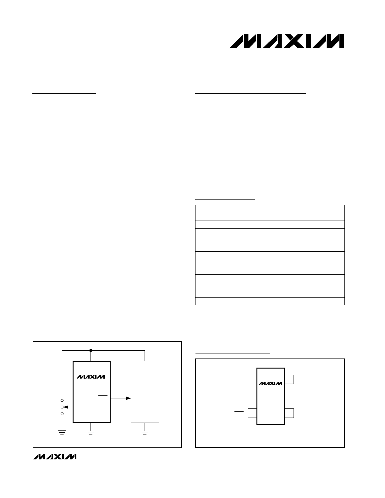
MAX821
MAX822
SOT143
TOP VIEW
( ) ARE FOR MAX822
Pin Configuration
MAX821
MAX822
V
CC
RESET
(RESET)
RESET
INPUT
GND
V
CC
GND
µP
( ) ARE FOR MAX822
SRT
20ms
100ms
1ms
__________Typical Operating Circuit
19-1122; Rev 1; 12/99
PART
MAX821LUS-T
MAX821MUS-T 4.38
4.63
NOMINAL VTH(V) TOP MARK*
AZ_ _
BA_ _
Ordering Information
* The first two letters in the package top mark identify the part,
while the remaining two letters are the lot-tracking code.
For free samples & the latest literature: http://www.maxim-ic.com, or phone 1-800-998-8800.
For small orders, phone 1-800-835-8769.
MAX821PUS-T 4.00 BM_ _
MAX821TUS-T 3.08 BB_ _
MAX821SUS-T 2.93 BC_ _
MAX821UUS-T 2.78 BL_ _
MAX821RUS-T 2.63 BD_ _
MAX822LUS-T
4.63 BF_ _
MAX822MUS-T 4.38 BG_ _
MAX822TUS-T 3.08 BH_ _
MAX822SUS-T 2.93 BJ_ _
MAX822RUS-T 2.63 BK_ _
Note: These parts are offered in the SOT143-4 package, in the
extended temperature range (-40°C to +85°C).

MAX821/MAX822
4-Pin µP Voltage Monitors with Pin-Selectable
Power-On Reset Timeout Delay
2 _______________________________________________________________________________________
ABSOLUTE MAXIMUM RATINGS
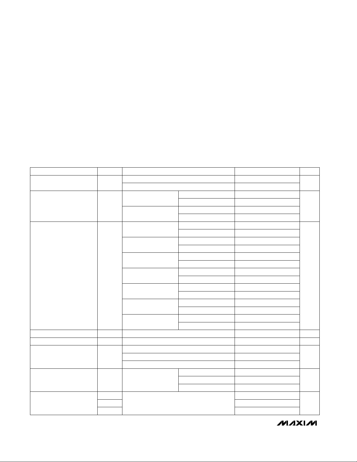
ELECTRICAL CHARACTERISTICS
(VCC= full range, TA= -40°C to +125°C, unless otherwise noted. Typical values are at TA= +25°C.)
Stresses beyond those listed under “Absolute Maximum Ratings” may cause permanent damage to the device. These are stress ratings only, and functional
operation of the device at these or any other conditions beyond those indicated in the operational sections of the specifications is not implied. Exposure to
absolute maximum rating conditions for extended periods may affect device reliability.
Terminal Voltage (with respect to GND)
V
CC
......................................................................-0.3V to 6.0V
All Other Inputs.......................................-0.3V to (V
CC
+ 0.3V)
Input Current, V
CC
, SRT......................................................20mA
Output Current, RESET or RESET .......................................20mA
Continuous Power Dissipation (T
A
= +70°C)
SOT143-4 (derate 4mW/°C above +70°C)...................320mW
Operating Temperature Range .........................-40°C to +125°C
Storage Temperature Range.............................-65°C to +160°C
Lead Temperature (soldering, 10sec).............................+300°C
SRT = unconnected
V
0.5V
CC
V
OPEN
SRT Input Threshold
0.9V
CC
V
IH
0.07V
CC
V
IL
ms
100 160 200
t
RP
Reset Active Timeout Period 20 32 40
2.5 7.0
V
1.2 5.5
1.0 5.5
VCCRange
0.5 0.8 1
µs50VCCto Reset Delay (Note 1)
ppm/°C30Reset Threshold Tempco
V
2.55 2.70
V
TH
Reset Threshold (Note 1)
12
1.8 5.5
µA
9
I
CC
Supply Current
2.59 2.63 2.66
UNITSMIN TYP MAXSYMBOLPARAMETER
TA= -40°C to +85°C
TA= 0°C to +70°C
VCCfalling at 1mV/µs
RESET = low for MAX821,
RESET = high for MAX822
MAX82_R
MAX82_L/M/P,
VCC= 5.5V, I
OUT
= 0
MAX82_R/S/T/U,
V
CC
= 5.5V, I
OUT
= 0
CONDITIONS
4.56 4.63 4.70
4.50 4.75
4.31 4.38 4.45
4.25 4.50
MAX82_L
MAX82_M
3.97 4.00 4.04
3.91 4.09
2.89 2.93 2.96
3.04 3.08 3.11
2.85 3.00
3.00 3.15
MAX82_P
2.74 2.78 2.81
2.70 2.85
MAX82_S
MAX82_U
µA
-1 1
SRT Input Current (Note 2) 100
-100
RESET = low for MAX821,
RESET = high for MAX822
SRT = GND
SRT = V
CC
TA= +25°C
TA= +25°C
TA= +25°C
TA= +25°C
TA= +25°C
MAX82_T
TA= +25°C
TA= +25°C
TA= +25°C
TA= +25°C
SRT = GND
SRT = unconnected
SRT = V
CC
TA= -40°C to +125°C
TA= -40°C to +125°C
TA= -40°C to +125°C
TA= -40°C to +125°C
TA= -40°C to +125°C
TA= -40°C to +125°C
TA= -40°C to +125°C
TA= T
MIN
to T
MAX
TA= T
MIN
to T
MAX

MAX821/MAX822
4-Pin µP Voltage Monitors with Pin-Selectable
Power-On Reset Timeout Delay
_______________________________________________________________________________________ 3
Note 1: RESET output for MAX821; RESET output for MAX822.
Note 2: During reset active timeout period only.
Note 3: Guaranteed by design.
ELECTRICAL CHARACTERISTICS (continued)
(VCC= full range, TA= -40°C to +125°C, unless otherwise noted. Typical values are at TA= +25°C.)
0.3
0.4
pF20
SRT Input Capacitance
(Note 3) (see Setting
the Reset Timeout Delay
section)
UNITSMIN TYP MAXSYMBOLPARAMETER
MAX821R/S/T/U only, I
SINK
= 1.2mA,
VCC= V
TH(MIN)
MAX821L/M/P only, I
SINK
= 3.2mA,
VCC= V
TH(MIN)
Internal
CONDITIONS
0.3
V
OL
0.3
I
SINK
= 50µA
0.3
0.4
MAX822R/S/T only, I
SINK
= 1.2mA,
V
CC
= V
TH(MAX)
MAX822L/M only, I
SINK
= 3.2mA,
V
CC
= VTH(MAX)
V
0.8V
CC
V
OH
RESET Output Voltage
(MAX821)
VCC-1.5
MAX821R/S/T/U only, I
SOURCE
= 500µA,
VCC≥ V
TH(MAX)
MAX821L/M/P only, I
SOURCE
= 800µA,
VCC≥ V
TH(MAX)
0.6
-40
RESET TIMEOUT PERIOD
vs. TEMPERATURE
0.7
MAX 821/822 TOC-04
TEMPERATURE (°C)
RESET TIMEOUT PERIOD (ms)
40 60 80
0.9
0.8
-20 20 100
1.0
0
SRT = GND
30
-40
RESET TIMEOUT PERIOD
vs. TEMPERATURE
32
31
MAX 821/822 TOC-05
TEMPERATURE (°C)
RESET TIMEOUT PERIOD (ms)
40 60 80
35
34
33
-20 20 100
36
0
SRT = V
CC
150
-40
RESET TIMEOUT PERIOD
vs. TEMPERATURE
160
155
MAX 821/822 TOC-06
TEMPERATURE (°C)
RESET TIMEOUT PERIOD (ms)
40 60 80
175
170
165
-20 20 100
180
0
SRT = UNCONNECTED
V
OL
V
V
OH
RESET Output Voltage
(MAX822)
0.8V
CC
I
SOURCE
= 150µA, 1.4V ≤ VCC≤ V
TH(MIN)
__________________________________________Typical Operating Characteristics
(TA = +25°C, unless otherwise noted.)
TA= 0°C to +70°C,
VCC≥ 1V
TA = -40°C to +85°C,
VCC≥ 1.2V
 Loading...