

Page 1
MAX705–MAX708/MAX813L
Low-Cost, µP Supervisory Circuits
________________________________________________________________
Maxim Integrated Products
1
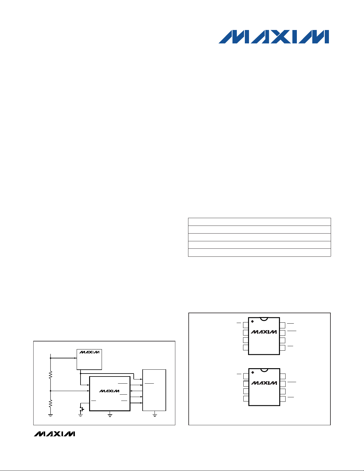
_________________Pin Configurations
V
CC
PFI
MR
PFO
WDO
RESET
UNREGULATED DC
PUSHBUTTON
SWITCH
PFI
I/O LINE
INTERRUPT
µP
MAX705
MAX706
MAX813L
MAX667
+5V DC LINEAR
REGULATOR
V
CC
RESET
NMI
__________Typical Operating Circuit
19-4334; Rev. 8; 3/10
_______________General Description
The MAX705-MAX708/MAX813L microprocessor (µP)
supervisory circuits reduce the complexity and number
of components required to monitor power-supply and
battery functions in µP systems. These devices significantly improve system reliability and accuracy compared to separate ICs or discrete components.
The MAX705/MAX706/MAX813L provide four functions:
1) A reset output during power-up, power-down, and
brownout conditions.
2) An independent watchdog output that goes low if
the watchdog input has not been toggled within 1.6
seconds.
3) A 1.25V threshold detector for power-fail warning,
low-battery detection, or for monitoring a power supply other than +5V.
4) An active-low manual-reset input.
The MAX707/MAX708 are the same as the MAX705/
MAX706, except an active-high reset is substituted for
the watchdog timer. The MAX813L is the same as the
MAX705, except RESET is provided instead of RESET.
Two supply-voltage monitor levels are available: The
MAX705/MAX707/MAX813L generate a reset pulse when
the supply voltage drops below 4.65V, while the
MAX706/MAX708 generate a reset pulse below 4.40V.
All four parts are available in 8-pin DIP, SO and µMAX
®
packages.
_______________________Applications
Computers
Controllers
Intelligent Instruments
Automotive Systems
Critical µP Power Monitoring
___________________________Features
o Available in Tiny µMAX Package
o Guaranteed RESET Valid at V
CC
= 1V
o Precision Supply-Voltage Monitor
4.65V in MAX705/MAX707/MAX813L
4.40V in MAX706/MAX708
o 200ms Reset Pulse Width
o Debounced TTL/CMOS-Compatible
Manual-Reset Input
o Independent Watchdog Timer—1.6s Timeout
(MAX705/MAX706)
o Active-High Reset Output
(MAX707/MAX708/MAX813L)
o Voltage Monitor for Power-Fail or Low-Battery
Warning
______________Ordering Information
PART TEMP RANGE PIN-PACKAGE
MAX705CPA
8 Plastic DIP
MAX705CSA 0°C to +70°C 8 SO
MAX705C/D 0°C to +70°C Dice*
Ordering Information continued at end of data sheet.
*
Dice are specified at TA= +25°C.
**
Contact factory for availability and processing to MIL-STD-883.
Devices in PDIP, SO and µMAX packages are available in both
leaded and lead-free packaging. Specify lead free by adding
the + symbol at the end of the part number when ordering.
Lead-free not available for CERDIP package.
0°C to +70°C
MAX705CUA 0°C to +70°C 8 µMAX
For pricing, delivery, and ordering information, please contact Maxim Direct at 1-888-629-4642,
or visit Maxim’s website at www.maxim-ic.com.
µMAX is a registered trademark of Maxim Integrated Products, Inc.
TOP VIEW
V
GND
MR
1
2
CC
MAX705
3
MAX706
MAX813L
PFI
4
WDO
8
RESET (RESET)
7
WDI
6
5
PFO
( ) ARE FOR MAX813L ONLY.
Pin Configurations continued at end of data sheet.
V
GND
DIP/SO
MR
1
2
CC
MAX707
3
PFI
MAX708
4
DIP/SO
RESET
8
RESET
7
N.C.
6
5
PFO
Page 2
MAX705–MAX708/MAX813L
Low-Cost, µP Supervisory Circuits
2 _______________________________________________________________________________________
Terminal Voltage (with respect to GND)
V
CC
.............................................. -0.3V to 6.0V
All Other Inputs (Note 1) ............... -0.3V to (V
CC
+ 0.3V)
Input Current
V
CC
...................................................... 20mA
GND .................................................... 20mA
Output Current (all outputs) ............................. 20mA
Continuous Power Dissipation (T
A
= +70°C)
Plastic DIP (derate 9.09mW/°C above +70°C) ....... 727mW
SO (derate 5.88mW/°C above +70°C) ............... 471mW
µMAX (derate 4.10mW/°C above +70°C) ............ 330mW
CERDIP (derate 8.00mW/°C above +70°C) .......... 640mW
Operating Temperature Ranges
MAX70_C__, MAX813LC__ .................... 0°C to +70°C
MAX70_E__, MAX813LE__ ................... -40°C to +85°C
MAX70_MJA ................................ -55°C to +125°C
Storage Temperature Range ................ -65°C to +160°C
Lead Temperature (soldering, 10s) ................... +300°C
Soldering Temperature (reflow)
Lead(Pb)-free.................................................................+260°C
Containing Lead(Pb)......................................................+240°C
ELECTRICAL CHARACTERISTICS
(VCC= 4.75V to 5.5V for MAX705/MAX707/MAX813L, VCC= 4.5V to 5.5V for MAX706/MAX708, TA= T
MIN
to T
MAX
, unless otherwise noted.)
Stresses beyond those listed under "Absolute Maximum Ratings" may cause permanent damage to the device. These are stress ratings only, and functional
operation of the device at these or any other conditions beyond those indicated in the operational sections of the specifications is not implied. Exposure to
absolute maximum rating conditions for extended periods may affect device reliability.
PARAMETER SYMBOL CONDITIONS MIN TYP MAX UNITS
Operating Voltage Range V
CC
MAX70_C 1.0 5.5
V
MAX813LC 1.1 5.5
MAX70_E/M, MAX813LE/M 1.2 5.5
Reset Threshold (Note 2) V
RT
MAX705, MAX707, MAX813L 4.50 4.65 4.75
MAX706, MAX708 4.25 4.40 4.50
40 mV
Reset Pulse Width (Note 2) t
RS
140 200 280 ms
RESET Output Voltage
I
SOURCE
= 800µA VCC- 1.5
V
ABSOLUTE MAXIMUM RATINGS
Note 1: The input voltage limits on PFI and MR can be exceeded if the input current is less than 10mA.
Reset Threshold Hysteresis (Note 2)
I
SINK
= 3.2mA 0.4
0.3
0.3
RESET Output Voltage
MAX707, MAX708, I
SOURCE
= 800µA
V
MAX707, MAX708, I
SINK
= 1.2mA 0.4
0.8
0.9
MAX813L
VCC- 1.5
0.4
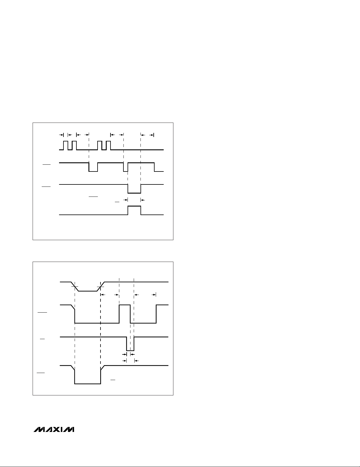
Watchdog Timeout Period t
WD
MAX705, MAX706, MAX813L
1.00 1.60 2.25 s
WDI Pulse Width t
WP
VIL= 0.4V, VIH= (VCC) (0.8) 50 ns
WDI Input Threshold
0.8
V
3.5
MAX70_C, VCC= 1V, I
SINK
= 50µA
MAX70_E/M, VCC= 1.2V, I
SINK
= 100µA
MAX813LC, I
SOURCE
= 4µA, VCC= 1.1V
MAX813LE/M, I
SOURCE
= 4µA, VCC= 1.2V
I
SOURCE
= 800µA
I
SINK
= 3.2mA
Low
High
WDI Input Current
MAX705, MAX706, MAX813L, WDI = V
CC
50 150
µA
MAX705, MAX706, MAX813L, WDI = 0V -150 -50
WDO Output Voltage
VCC- 1.5
V
0.4
MAX705, MAX706, MAX813L,
V
CC
= 5V
MAX705, MAX706, MAX813L,
I
SOURCE
= 800µA
MAX705, MAX706, MAX813L,
I
SINK
= 1.2mA
V
VCC- 1.5
MAX707C, MAX708C 50 350
MAX707E/M, MAX708E/M 50 500
Supply Current I
SUPPLY
MAX705C, MAX706C, MAX813LC 150 350
µA
MAX705E/M, MAX706E/M, MAX813LE/M 150 500
Page 3
MAX705–MAX708/MAX813L
Low-Cost, µP Supervisory Circuits
_______________________________________________________________________________________ 3
ELECTRICAL CHARACTERISTICS (continued)
(VCC= 4.75V to 5.5V for MAX705/MAX707/MAX813L, VCC= 4.5V to 5.5V for MAX706/MAX708, TA= T
MIN
to T
MAX
, unless otherwise noted.)
PARAMETER
SYMBOL CONDITIONS MIN TYP MAX UNITS
0.8
V
2.0
MR Pull-Up Current MR = 0V
100 250 600 µA
MR Pulse Width
t
MR
150 ns
Low
High
MR Input Threshold
MR to Reset Out Delay (Note 2)
t
MD
250 ns
PFI Input Threshold VCC= 5V 1.20 1.25 1.30 V
PFI Input Current -25.00 +0.01 +25.00 nA
PFO Output Voltage
I
SOURCE
= 800µA VCC- 1.5
V
I
SINK
= 3.2mA 0.4
Note 2: Applies to both RESET in the MAX705–MAX708 and RESET in the MAX707/MAX708/MAX813L.
Page 4
MAX705–MAX708/MAX813L
Low-Cost, µP Supervisory Circuits
4 _______________________________________________________________________________________
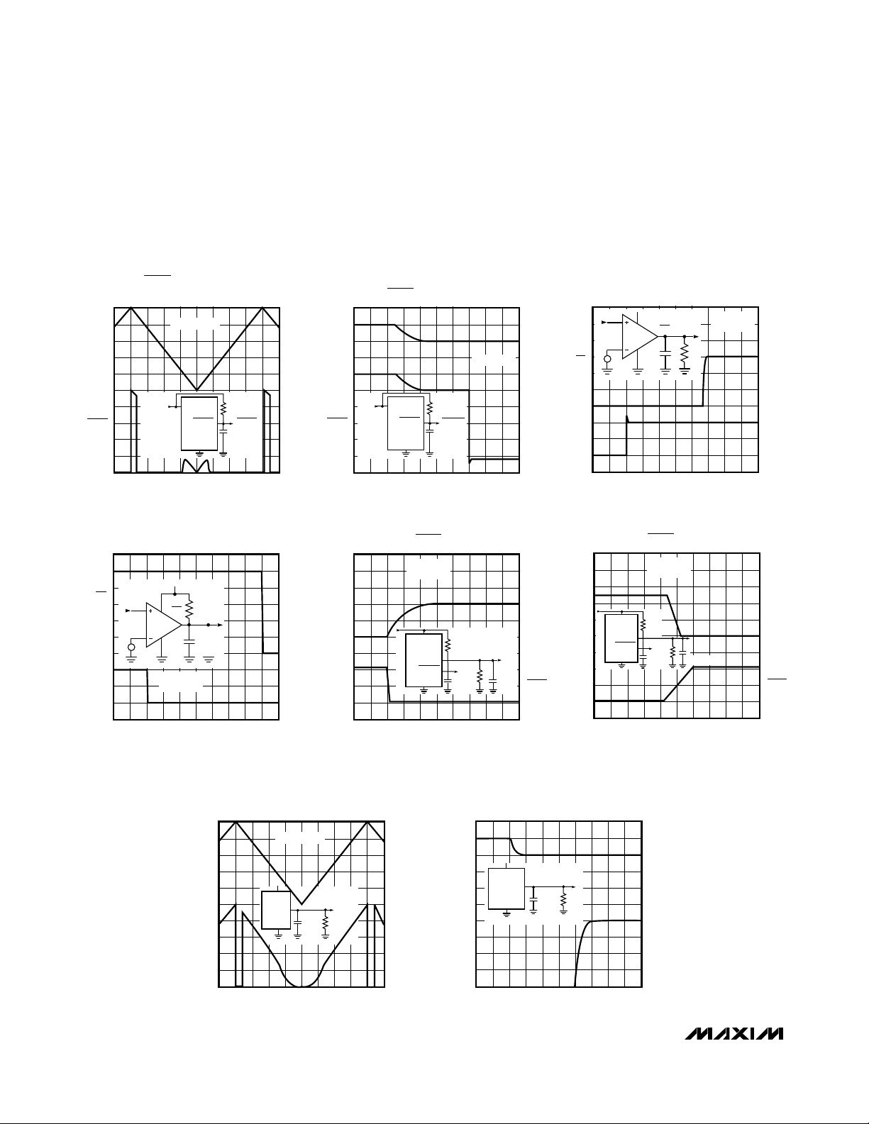
__________________________________________Typical Operating Characteristics
MAX707/MAX708/MAX813L
RESET OUTPUT VOLTAGE
vs. SUPPLY VOLTAGE
500ms/div
V
CC
0V
RESET
0V
+5V
1V/div
+5V
1V/div
TA = +25°C
GND
RESET
V
CC
330pF
10k
Ω
MAX813L
RESET RESPONSE TIME
2µs/div
+5V
V
CC
0V
0V
+4V
+4V
GND
RESET
V
CC
330pF
10k
Ω
MAX705/MAX707
RESET OUTPUT VOLTAGE
vs. SUPPLY VOLTAGE
500ms/div
V
CC
0V
RESET
0V
+5V
1V/div
+5V
1V/div
V
CC
GND
RESET
V
CC
2k
Ω
RESET
330pF
TA = +25°C
MAX705/MAX707
RESET RESPONSE TIME
2µs/div
V
CC
+5V
RESET
+5V
+4V
1V/div
0V
TA = +25°C
V
CC
GND
RESET
V
CC
10k
Ω
RESET
30pF
POWER-FAIL COMPARATOR
DE-ASSERTION RESPONSE TIME
400ns/div
PFI
+1.20V
PFO
0V
+3V
+1.30V
VCC = +5V
T
A
= +25°C
+5V
PFO
30pF
1k
Ω
+1.25V
PFI
POWER-FAIL COMPARATOR
ASSERTION RESPONSE TIME
400ns/div
PFI
+1.30V
PFO
+5V
0V
+1.20V
1V/div 50mV/div
+5V
PFO
30pF
1k
Ω
+1.25V
PFI
VCC = +5V
T
A
= +25°C
MAX707
RESET, RESET ASSERTION
400ns/div
0V
+5V
RESET
RESET
1V/div
VCC = V
RT
TA = +25°C
+5V
0V
V
CC
GND
RESET
10k
Ω
330pF
RESET
10k
Ω
330pF
MAX707
RESET, RESET DE-ASSERTION
400ns/div
0V
+5V
RESET
RESET
2V/div
VCC = V
RT
TA = +25°C
+5V
0V
V
CC
GND
RESET
RESET
10k
Ω
330pF
10k
Ω
330pF
Page 5
MAX705–MAX708/MAX813L
Low-Cost, µP Supervisory Circuits
_______________________________________________________________________________________ 5
______________________________________________________________Pin Description
Watchdog Output pulls low when the internal watchdog timer finishes its 1.6sec count and does not go
high again until the watchdog is cleared. WDO also
goes low during low-line conditions. Whenever V
CC
is
below the reset threshold, WDO stays low; however,
unlike RESET, WDO does not have a minimum pulse
width. As soon as V
CC
rises above the reset thresh-
old, WDO goes high with no delay.
Active-High Reset Output is the inverse of RESET.
Whenever RESET is high, RESET is low, and vice
versa (Figure 2). The MAX813L has a RESET output
only.
Active-Low Reset Output pulses low for 200ms when
triggered, and stays low whenever V
CC
is below the
reset threshold (4.65V in the MAX705 and 4.40V in the
MAX706). It remains low for 200ms after V
CC
rises
above the reset threshold or MR goes from low to high
(Figure 3). A watchdog timeout will not trigger RESET
unless WDO is connected to MR.
Watchdog Input. If WDI remains high or low for
1.6sec, the internal watchdog timer runs out and
WDO goes low (Figure 1). Floating WDI or connecting WDI to a high-impedance three-state buffer disables the watchdog feature. The internal watchdog
timer clears whenever reset is asserted, WDI is threestated, or WDI sees a rising or falling edge.
Power-Fail Output goes low and sinks current when
PFI is less than 1.25V; otherwise PFO stays high.
Power-Fail Voltage Monitor Input. When PFI is less
than 1.25V, PFO goes low. Connect PFI to GND or
V
CC
when not used.
FUNCTION
MAX705/MAX706
RESET78—
WDO
8—8
RESET
—77
No ConnectN.C.—6—
WDI6—6
PFO
555
PFI444
0V Ground Reference for all signalsGND333
+5V Supply Input
V
CC
222
NAME
DIP/SODIP/SODIP/SO
MAX707/MAX708
PIN
—
2
1
—
8
7
6
5
4
µMAX
2
—
1
—
—
7
6
5
4
µMAX
1
2
—
—
8
7
6
5
4
µMAX
MAX813L
Manual-Reset Input triggers a reset pulse when
pulled below 0.8V. This active-low input has an internal 250µA pull-up current. It can be driven from a TTL
or CMOS logic line as well as shorted to ground with
a switch.
MR
111 3 3 3
Page 6

MAX705–MAX708/MAX813L
_______________Detailed Description
Reset Output
A microprocessor’s (µP’s) reset input starts the µP in a
known state. Whenever the µP is in an unknown state, it
should be held in reset. The MAX705-MAX708/MAX813L
assert reset during power-up and prevent code execution errors during power-down or brownout conditions.
On power-up, once VCCreaches 1V, RESET is a guaranteed logic low of 0.4V or less. As VCCrises, RESET stays
low. When VCCrises above the reset threshold, an internal timer releases RESET after about 200ms. RESET pulses low whenever V
CC
dips below the reset threshold, i.e.
brownout condition. If brownout occurs in the middle of
a previously initiated reset pulse, the pulse continues for
at least another 140ms. On power-down, once V
CC
falls
below the reset threshold, RESET stays low and is guaranteed to be 0.4V or less until V
CC
drops below 1V.
The MAX707/MAX708/MAX813L active-high RESET output
is simply the complement of the RESET output, and is
guaranteed to be valid with VCCdown to 1.1V. Some µPs,
such as Intel’s 80C51, require an active-high reset pulse.
Watchdog Timer
The MAX705/MAX706/MAX813L watchdog circuit monitors the µP’s activity. If the µP does not toggle the watchdog input (WDI) within 1.6sec and WDI is not three-stated, WDO goes low. As long as RESET is asserted or the
WDI input is three-stated, the watchdog timer will stay
cleared and will not count. As soon as reset is released
and WDI is driven high or low, the timer will start counting.
Pulses as short as 50ns can be detected.
Typically, WDO will be connected to the non-maskable
interrupt input (NMI) of a µP. When V
CC
drops below
the reset threshold, WDO will go low whether or not the
watchdog timer has timed out yet. Normally this would
trigger an NMI interrupt, but RESET goes low simultaneously, and thus overrides the NMI interrupt.
If WDI is left unconnected, WDO can be used as a lowline output. Since floating WDI disables the internal
timer, WDO goes low only when VCCfalls below the
reset threshold, thus functioning as a low-line output.
The MAX705/MAX706 have a watchdog timer and a
RESET output. The MAX707/MAX708 have both activehigh and active-low reset outputs. The MAX813L has
both an active-high reset output and a watchdog timer.
Manual Reset
The manual-reset input (MR) allows reset to be triggered
by a pushbutton switch. The switch is effectively
debounced by the 140ms minimum reset pulse width.
MR is TTL/CMOS logic compatible, so it can be driven by
an external logic line. MR can be used to force a watchdog timeout to generate a reset pulse in the MAX705/
MAX706/MAX813L. Simply connect WDO to MR.
Low-Cost, µP Supervisory Circuits
6 _______________________________________________________________________________________
Figure 1. MAX705/MAX706/MAX813L Block Diagram
Figure 2. MAX707/MAX708 Block Diagram
WATCHDOG
6
1
2
4
TRANSITION
DETECTOR
V
CC
250µA
4.65V*
1.25V
WDI
MR
V
CC
PFI
* 4.40V FOR MAX7O6.
( ) ARE FOR MAX813L ONLY.
WATCHDOG
TIMER
TIMEBASE FOR
RESET AND
WATCHDOG
RESET
GENERATOR
MAX705
MAX706
MAX813L
3
GND
8
WDO
MR
7
RESET
(RESET)
5
PFO
V
PFI
V
CC
1
2
CC
4
* 4.40V FOR MAX7O6.
250µA
4.65V*
1.25V
RESET
GENERATOR
3
MAX707
MAX708
GND
8
RESET
7
RESET
5
PFO
Page 7
Power-Fail Comparator
The power-fail comparator can be used for various purposes because its output and noninverting input are
not internally connected. The inverting input is internally connected to a 1.25V reference.
To build an early-warning circuit for power failure, connect the PFI pin to a voltage divider (see
Typical
Operating Circuit
). Choose the voltage divider ratio so
that the voltage at PFI falls below 1.25V just before the
+5V regulator drops out. Use PFO to interrupt the µP
so it can prepare for an orderly power-down.
__________Applications Information
Ensuring a Valid RESET
Output Down to V
CC
= 0V
When VCCfalls below 1V, the MAX705-MAX708 RESET
output no longer sinks current—it becomes an open circuit. High-impedance CMOS logic inputs can drift to
undetermined voltages if left undriven. If a pull-down
resistor is added to the RESET pin as shown in Figure 5,
any stray charge or leakage currents will be drained to
ground, holding RESET low. Resistor value (R1) is not
critical. It should be about 100kΩ, large enough not to
load RESET and small enough to pull RESET to ground.
Monitoring Voltages Other Than the
Unregulated DC Input
Monitor voltages other than the unregulated DC by
connecting a voltage divider to PFI and adjusting the
ratio appropriately. If required, add hysteresis by connecting a resistor (with a value approximately 10 times
the sum of the two resistors in the potential divider network) between PFI and PFO. A capacitor between PFI
and GND will reduce the power-fail circuit’s sensitivity
to high-frequency noise on the line being monitored.
RESET can be asserted on other voltages in addition to
the +5V VCCline. Connect PFO to MR to initiate a RESET
pulse when PFI drops below 1.25V. Figure 6 shows the
MAX705-MAX708 configured to assert RESET when the
+5V supply falls below the reset threshold, or when the
+12V supply falls below approximately 11V.
Monitoring a Negative Voltage
The power-fail comparator can also monitor a negative
supply rail (Figure 7). When the negative rail is good (a
negative voltage of large magnitude), PFO is low, and
when the negative rail is degraded (a negative voltage
of lesser magnitude), PFO is high. By adding the resistors and transistor as shown, a high PFO triggers reset.
As long as PFO remains high, the MAX705MAX708/MAX813L will keep reset asserted (RESET =
low, RESET = high). Note that this circuit’s accuracy
depends on the PFI threshold tolerance, the VCCline,
and the resistors.
MAX705–MAX708/MAX813L
Low-Cost, µP Supervisory Circuits
_______________________________________________________________________________________ 7
Figure 3. MAX705/MAX706/MAX813L Watchdog Timing
Figure 4. MAX705/MAX706 RESET, MR, and WDO Timing with
WDI Three-Stated. The MAX707/MAX708/MAX813L RESET
output is the inverse of RESET shown.
t
WP
t
WD
+5V
WDI
0V
+5V
WDO
0V
+5V
RESET
0V
RESET EXTERNALLY
V
RT
TRIGGERED BY MR
V
RT
+5V
(RESET)
0V
( ) ARE FOR MAX813L ONLY.
V
CC
+5V
RESET
0V
+5V
MR
0V
+5V
WDO
0V
t
WD
t
RS
MR EXTERNALLY DRIVEN LOW
t
WD
t
RS
t
RS
t
MD
t
MR
Page 8

MAX705–MAX708/MAX813L
Interfacing to µPs with
Bidirectional Reset Pins
µPs with bidirectional reset pins, such as the Motorola
68HC11 series, can contend with the MAX705-MAX708
RESET output. If, for example, the RESET output is driven
high and the µP wants to pull it low, indeterminate logic
levels may result. To correct this, connect a 4.7kΩ
resistor between the RESET output and the µP reset I/O,
as in Figure 8. Buffer the RESET output to other system
components.
Low-Cost, µP Supervisory Circuits
8 _______________________________________________________________________________________
Figure 7. Monitoring a Negative Voltage
Figure 8. Interfacing to µPs with Bidirectional Reset I/O
Figure 5. RESET Valid to Ground Circuit
Figure 6. Monitoring Both +5V and +12V
MAX70_
RESET
R1
+5V
V
CC
MAX70_
GND
MR
100kΩ
PFO
RESET
R1
PFI
R2
100kΩ
2N3904
TO µP
1MΩ
1%
130kΩ
1%
V
MAX70_
+12V
+12V Reset
Threshold at +25°C
CC
+5V
PARAMETER
RESET
V
RESET
CC
TO µP
MAX70_
MR
PFI
MIN TYP
10.67
BUFFERED RESET TO OTHER SYSTEM COMPONENTS
4.7kΩ
GND
10.87
PFO
MAX UNIT
11.50 V
RESET
V
CC
µP
V-
MR
PFO
+5V
+5V
0V
0V
−
5 1.25
R1
V-
1.25 V
=
−
R2
V
TRIP 0V
TRIP
,V
TRIP
0
<
GND
GND
Page 9

MAX705–MAX708/MAX813L
Low-Cost, µP Supervisory Circuits
_______________________________________________________________________________________ 9
__Ordering Information (continued)
8 CERDIP**-55°C to +125°CMAX813LMJA
8 Plastic DIP0°C to +70°C
MAX708CPA
8SO0°C to +70°CMAX708CSA
Dice*0°C to +70°CMAX708C/D
8 Plastic DIP-40°C to +85°CMAX708EPA
8SO-40°C to +85°CMAX708ESA
8 CERDIP**-55°C to +125°CMAX708MJA
8 Plastic DIP0°C to +70°C
MAX813LCPA
8SO0°C to +70°CMAX813LCSA
Dice*0°C to +70°CMAX813LC/D
8 Plastic DIP-40°C to +85°CMAX813LEPA
8SO-40°C to +85°CMAX813LESA
8 CERDIP**-55°C to +125°CMAX707MJA
8SO-40°C to +85°CMAX707ESA
8 Plastic DIP-40°C to +85°CMAX707EPA
Dice*0°C to +70°CMAX707C/D
8SO0°C to +70°CMAX707CSA
8 Plastic DIP0°C to +70°C
MAX707CPA
8 CERDIP**-55°C to +125°CMAX706MJA
8SO-40°C to +85°CMAX706ESA
8 Plastic DIP-40°C to +85°CMAX706EPA
8 CERDIP**-55°C to +125°CMAX705MJA
8SO-40°C to +85°CMAX705ESA
8 Plastic DIP-40°C to +85°CMAX705EPA
PIN-PACKAGETEMP RANGEPART
Dice*0°C to +70°CMAX706C/D
8SO0°C to +70°CMAX706CSA
8 Plastic DIP0°C to +70°C
MAX706CPA
8 µMAX0°C to +70°CMAX706CUA
8 µMAX0°C to +70°CMAX707CUA
8 µMAX0°C to +70°CMAX708CUA
8 µMAX0°C to +70°CMAX813LCUA
_____Pin Configurations (continued)
____________________Chip Topography
( ) ARE FOR MAX813L ONLY.
TRANSISTOR COUNT: 572
SUBSTRATE MUST BE LEFT UNCONNECTED.
8 µMAX-40°C to +85°CMAX705EUA
8 µMAX-40°C to +85°CMAX706EUA
8 µMAX-40°C to +85°CMAX707EUA
8 µMAX-40°C to +85°CMAX708EUA
8 µMAX-40°C to +85°CMAX813LEUA
*
Dice are specified at TA= +25°C.
**
Contact factory for availability and processing to MIL-STD-883.
Devices in PDIP, SO and µMAX packages are available in both
leaded and lead-free packaging. Specify lead free by adding
the + symbol at the end of the part number when ordering.
Lead free not available for CERDIP package.
TOP VIEW
(RESET) RESET
( ) ARE FOR MAX813L ONLY.
WDO
MR
V
RESET
RESET
MR
V
1
2
MAX705
3
MAX706
MAX813L
4
CC
µ
MAX
1
2
MAX707
3
MAX708
4
CC
µ
MAX
WDI
8
7
PFO
PFI
6
GND
5
N.C.
8
PFO
7
PFI
6
5
GND
MR
V
CC
GND
WDO/RESET
PFO
PFI
0.074"
(1.88mm)
RESET (RESET)
WDI/N.C.
0.051"
(1.30mm)
Page 10

MAX705–MAX708/MAX813L
Low-Cost, µP Supervisory Circuits
10 ______________________________________________________________________________________
1000-up ($)
Price
†
Pins
max (typ)
µA
Backup Mode
SUPPLY
I
max (typ)
mA
Operating Mode
SUPPLY
I
Output
Battery-On
Output
Low-Line
Input
Manual-Reset
Comparator
Power-Fail
Protect
Write
–C—E–
Max (Ω)
On Resistance
BATT
OUT
-to-V
V
Max (Ω)
OUT
Valid
= 1V
-to-V
CC
On Resistance
CC
V
Switch
Backup-Battery
Output
Watchdog
Separate
(sec), if Available
Timeout Period
Watchdog
Nominal
to V
–R—E—S—E—T–
Reset
Active-High
Reset
Active-Low
Pulse Width (ms)
Minimum Reset
Threshold (V)
Nominal Reset
Number
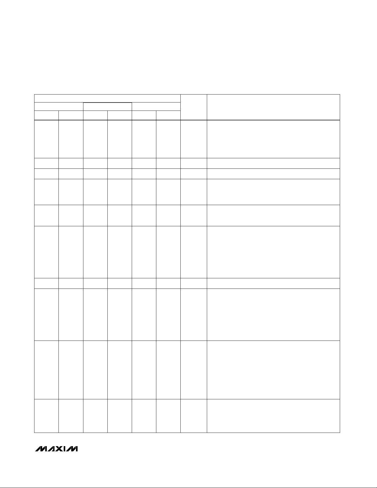
___________________________________________µP Supervisory Circuits
Part
MAX1232 4.37/4.62 250 ✔✔✔0.15/0.6/1.2 ✔ 0.2(0.05) 8 1.71
MAX690A/692A 4.65/4.40 140 ✔✔1.6 ✔ 10 400 ✔ 0.35(0.2) 5(0.05) 8 3.26
MAX690R/S/T 2.63/2.93/3.08 140 ✔✔1.6 ✔ 6 400 ✔ 0.5(0.4) 1(0.4) 8 3.23
MAX691A/693A 4.65/4.40 140/adj. ✔✔ ✔1.6/adj. ✔✔1.2 25 ✔/10ns ✔✔0.1(0.035) 5(0.04) 16 3.61
MAX1691 The MAX1691 is a module with the MAX691A and a 125mAh lithium battery 16 ††
MAX696 Adj. 35/adj. ✔✔ 1.6/adj. ✔✔ ✔ ✔ 16 3.55
MAX697 Adj. 35/adj. ✔✔ 1.6/adj. ✔✔✔ 16 3.58
MAX700 4.65/adj. 200 ✔✔ ✔ 0.2(0.1) 8 2.17
MAX703/704 4.65/4.40 140 ✔✔ ✔10 400 ✔✔ 0.35(0.2) 5(0.05) 8 1.38*
MAX704R/S/T 2.63/2.93/3.08 140 ✔✔ ✔6 400 ✔✔ 0.5(0.4) 1(0.4) 8 2.93
MAX705/706 4.65/4.40 140 ✔✔1.6 ✔✔✔0.35(0.2) 8 1.02*
MAX706P 2.63 140 ✔✔1.6 ✔✔✔0.35(0.2) 8 1.71
MAX706R/S/T 2.63/2.93/3.08 140 ✔✔1.6 ✔✔✔0.35(0.2) 8 1.71
MAX707/708 4.65/4.40 140 ✔✔ ✔ ✔ ✔ 0.35(0.2) 8 0.88*
MAX708R/S/T 2.63/2.93/3.08 140 ✔✔ ✔ ✔ ✔ 0.35(0.2) 8 1.63
MAX791 4.65 140 ✔✔ ✔1 ✔✔1.2 25 ✔/10ns ✔ ✔✔✔0.15(0.06) 5(0.04) 16 3.90
MAX792L/M/R/S/T 4.65/4.40/ 140 ✔✔ ✔1 ✔✔/10ns ✔✔✔ 0.15(0.07) 16 3.42
2.63/2.93/3.08
MAX793R/S/U/T 2.63/2.93/3.07/3.08 140 ✔✔ ✔1.6 ✔✔TBD TBD ✔✔✔✔ TBD TBD 16 ††
MAX794 Adj. 140 ✔✔ ✔1.6 ✔✔TBD TBD ✔✔✔✔ TBD TBD 16 ††
MAX795R/S/U/T 2.63/2.93/3.07/3.08 140 ✔✔ ✔TBD TBD ✔✔TBD TBD 8 ††
MAX800L/M 4.60/4.40 140 ✔✔ ✔1.6/adj. ✔✔1.2 25 ✔/10ns ✔/±2% ✔ 0.1(0.035) 5(0.04) 16 3.88
MAX801L/N/M 4.68/4.58/4.43 140 ✔/±1.5% ✔ 1.6 ✔ TBD TBD ✔ TBD TBD 8 ††
MAX802L/M/R/S/T 4.60/4.40/ 140 ✔✔1.6 ✔ 10 400 ✔/±2% 0.35(0.2) 5(0.05) 8 3.59
2.63/2.93/3.08
2.63/2.93/3.08
MAX804R/S/T 2.63/2.93/3.08 140 ✔✔1.6 ✔ 6 400 ✔/±2% 0.5(0.4) 1(0.4) 8 3.66
MAX805L/M/R/S/T 4.65/4.40/ 140 ✔✔1.6 ✔ 10 400 ✔ 0.35(0.2) 5(0.05) 8 3.26
MAX806R/S/T 2.63/2.93/3.08 140 ✔✔ ✔ ✔6 400 ✔/±2% ✔ 0.5(0.4) 1(0.4) 8 3.90
MAX807L/N/M 4.68/4.58/4.43 140 ✔/±1.5% ✔/±1.5% ✔ 1.6 ✔✔TBD TBD ✔ ✔ ✔✔✔TBD TBD 8 ††
MAX808L/N/M 4.68/4.58/4.43 140 ✔/±1.5% ✔✔TBD TBD ✔✔TBD TBD 16 ††
MAX809L/M/R/S/T 4.65/4.40/ 140 ✔✔ 0.06(0.024) 3 ††
2.63/2.93/3.08
2.63/2.93/3.08
MAX810L/M/R/S/T 4.65/4.40/ 140 ✔✔ 0.06(0.024) 3 ††
MAX813L 4.65 140 ✔✔1.6 ✔✔/±2% ✔ 0.35(0.2) 8 1.02*
2.63/2.93/3.08
MAX814K/L/N/T 4.80/4.70/4.55/3.03 140 ✔/±1% ✔/±1% ✔✔/±2% ✔✔ TBD TBD 8 ††
MXD1210 4.37/4.62 ✔ 2.5 667 ✔ 0.5(0.23) 0.1(0.002) 8 2.44
MAX815K/L/N/T 4.80/4.70/4.55/3.03 140 ✔/±1% ✔ 1.6 ✔✔/±2% ✔ TBD TBD 8 ††
MAX816 Adj./±1% 140 ✔✔✔ ✔/±2% ✔ TBD TBD 8 ††
MAX820L/M/R/S/T 4.65/4.40/ 140 ✔✔ ✔1 ✔✔/10ns ✔/±2% ✔✔ 0.15(0.07) 16 3.82
Prices provided are for design guidance and are FOB USA (unless otherwise noted). International prices will differ due to local duties, taxes, and exchange rates.
Future product—contact factory for pricing and availability. Specifications are preliminary.
†
††
* 25,000 pc. price, factory direct
Page 11
MAX705–MAX708/MAX813L
Low-Cost, µP Supervisory Circuits
______________________________________________________________________________________ 11
PACKAGE TYPE PACKAGE CODE DOCUMENT NO.
8 µMAX U8-1
21-0036
8 Plastic DIP P8-1
21-0043
8 SO S8-1
21-0041
Package Information
For the latest package outline information and land patterns, go to www.maxim-ic.com/packages. Note that a “+”, “#”, or “-” in the
package code indicates RoHS status only. Package drawings may show a different suffix character, but the drawing pertains to the
package regardless of RoHS status.
Page 12

MAX705–MAX708/MAX813L
Low-Cost, µP Supervisory Circuits
Maxim cannot assume responsibility for use of any circuitry other than circuitry entirely embodied in a Maxim product. No circuit patent licenses are
implied. Maxim reserves the right to change the circuitry and specifications without notice at any time.
12
____________________Maxim Integrated Products, 120 San Gabriel Drive, Sunnyvale, CA 94086 408-737-7600
© 2010 Maxim Integrated Products Maxim is a registered trademark of Maxim Integrated Products, Inc.
Revision History
REVISION
NUMBER
0 2/92 Initial release —
8 3/10
REVISION
DATE
DESCRIPTION
Updated the Features, Absolute Maximum Ratings, Typical Operating
Characteristics, Figures 3, 7, 8, and the Package Information sections.
PAGES
CHANGED
1, 2, 4, 7, 8, 10
 Loading...