

Page 1
19-0433; Rev 0; 9/95
Full-Featured µP Supervisory Circuit with
±1.5% Reset Accuracy
_______________General Description
The MAX807 microprocessor (µP) supervisory circuit
reduces the complexity and number of components
needed to monitor power-supply and battery-control functions in µP systems. A 70µA supply current makes the
MAX807 ideal for use in portable equipment, while a 2ns
chip-enable propagation delay and 250mA output current
capability (20mA in battery-backup mode) make it suitable for larger, higher-performance equipment.
The MAX807 comes in 16-pin DIP and SO packages, and
provides the following functions:
1) µP reset. The active-low RESEToutput is asserted during power-up, power-down, and brownout conditions,
and is guaranteed to be in the correct state for V
down to 1V.
CC
2) Active-high RESET output.
3) Manual-reset input.
4) Two-stage power-fail warning. A separate low-line
comparator compares VCCto a threshold 52mV above
the reset threshold. This low-line comparator is more
accurate than those in previous µP supervisors.
5) Backup-battery switchover for CMOS RAM, real-time
clocks, µPs, or other low-power logic.
6) Write protection of CMOS RAM or EEPROM.
7) 2.275V threshold detector—provides for power-fail
warning and low-battery detection, or monitors a
power supply other than +5V.
8) BATT OK status flag indicates that the backup-battery
voltage is above 2.275V.
9) Watchdog-fault output—asserted if the watchdog input
has not been toggled within a preset timeout period.
________________________Applications
Computers
Controllers
Intelligent Instruments
Critical µP Power Monitoring
Portable/Battery-Powered Equipment
____________________________Features
♦ Precision 4.675V (MAX807L) or 4.425V
(MAX807M), or 4.575V (MAX807N) Voltage
Monitoring
♦ 200ms Power OK / Reset Time Delay
♦ RESET
and RESET Outputs
♦ Independent Watchdog Timer
♦ 1µA Standby Current
♦ Power Switching:
250mA in V
CC
Mode
20mA in Battery-Backup Mode
♦ On-Board Gating of Chip-Enable Signals:
2ns CE Gate Propagation Delay
♦ MaxCap™ and SuperCap™ Compatible
♦ Voltage Monitor for Power-Fail
♦ Backup-Battery Monitor
♦ Guaranteed RESET
Valid to VCC= 1V
♦ ±1.5% Low-line Threshold Accuracy 52mV above
Reset Threshold
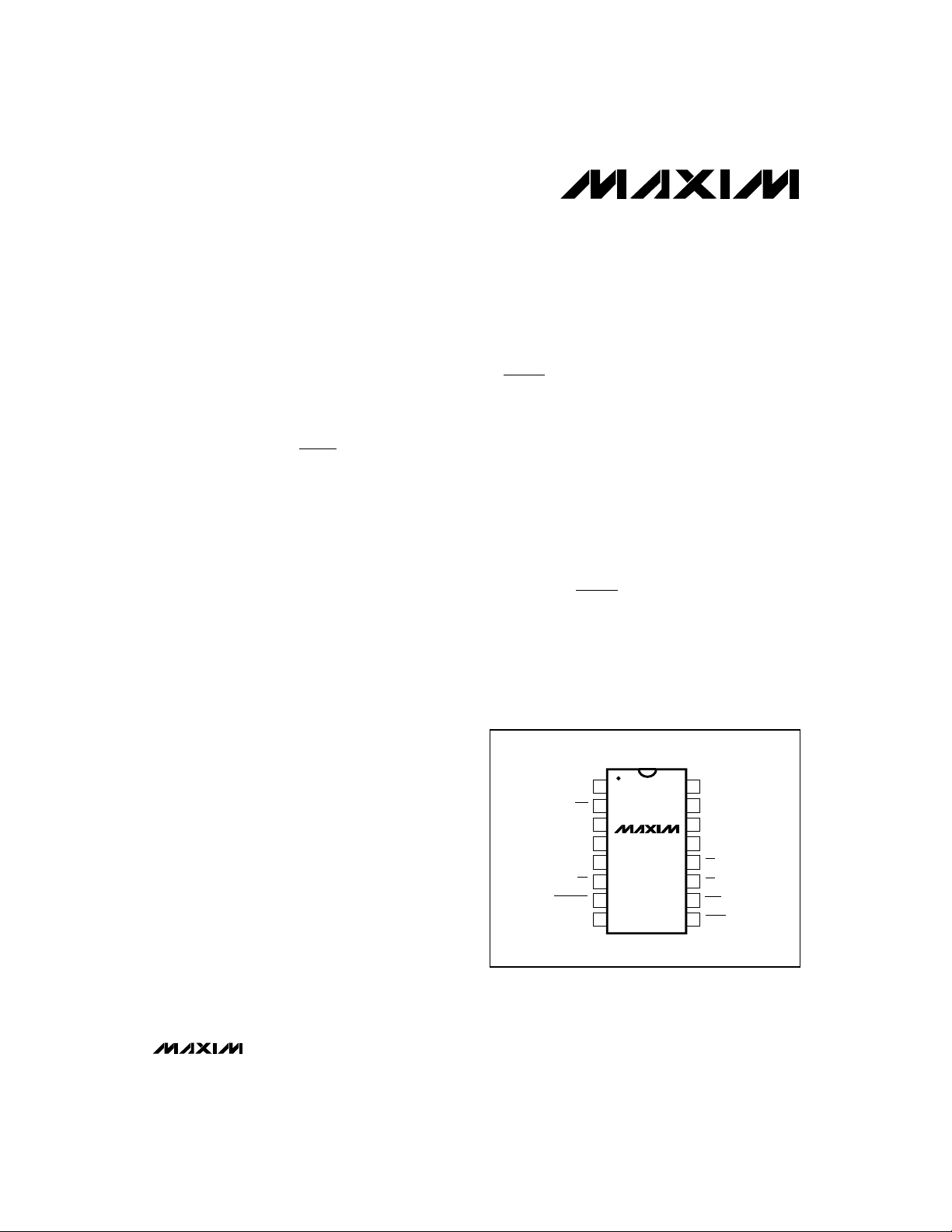
__________________Pin Configuration
TOP VIEW
WDI
GND
LOW LINE
RESET
PFO
V
PFI
1
2
CC
3
MAX807
4
5
MR
6
7
8
16
15
14
13
12
11
10
9
OUT
BATT OK
BATT
BATT ON
CE IN
CE OUT
WDO
RESET
MAX807L/M/N
DIP/SO
Ordering Information and Typical Operating Circuit appear at end of data sheet.
SuperCap is a trademark of Baknor Industries. MaxCap is a trademark of The Carborundum Corp.
________________________________________________________________
Maxim Integrated Products
Call toll free 1-800-998-8800 for free samples or literature.
1
Page 2
Full-Featured µP Supervisory Circuit with
±1.5% Reset Accuracy
ABSOLUTE MAXIMUM RATINGS
Input Voltages (with respect to GND)
..........................................................................-0.3V to 6V
V
CC
.......................................................................-0.3V to 6V
V
BATT
All Other Inputs......................................-0.3V to (V
Input Current
Peak ...........................................................................1.0A
V
CC
Continuous .............................................................500mA
V
CC
Peak......................................................................250mA
I
BATT
Continuous .............................................................50mA
I
BATT
GND.................................................................................50mA
OUT
+ 0.3V)
All Other Inputs................................................................50mA
Stresses beyond those listed under “Absolute Maximum Ratings” may cause permanent damage to the device. These are stress ratings only, and functional
operation of the device at these or any other conditions beyond those indicated in the operational sections of the specifications is not implied. Exposure to
MAX807L/M/N
absolute maximum rating conditions for extended periods may affect device reliability.
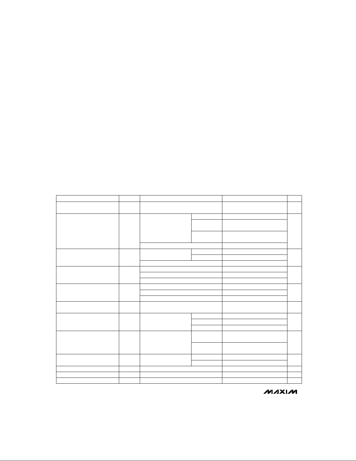
ELECTRICAL CHARACTERISTICS
(VCC= 4.60V to 5.5V for the MAX807L, VCC= 4.50V to 5.5V for the MAX807N, VCC= 4.35V to 5.5V for the MAX807M,
V
= 2.8V, V
BATT
Operating Voltage Range
, VCC(Note 1)
V
BATT
V
in Normal Operating
OUT
Mode
VCCto OUT On-Resistance
V
in Battery-Backup Mode V
OUT
BATT to OUT On-Resistance 12 25
Supply Current in Normal
Operating Mode (excludes I
Supply Current in BatteryBackup Mode (excludes I
(Note 2)
BATT Standby Current (Note 3)
Battery-Switchover Threshold
Battery-Switchover Hysteresis 50
BATT ON Output, Low Voltage V
= 0V, TA= T
PFI
OUT
OUT
)
MIN
to T
. Typical values are tested with VCC= 5V and TA= +25°C, unless otherwise noted.)
MAX
VCC= 4.5V
VCC= 3V, V
BATT
VCC= 4.5V,
I
= 250mA
OUT
VCC= 3V, I
V
BATT
V
BATT
V
BATT
V
BATT
V
BATT
V
BATT
OUT
= 4.5V, I
= 2.8V, I
= 2.0V, I
= 4.5V, I
= 2.8V, I
= 2.0V, I
)
VCC= 0V, V
V
BATT
V
BATT
RST (max)
BATT
+ 0.2V ≤ V
= 2.8V
, I
SINK
SOURCE
Continuous Power Dissipation (T
Plastic DIP (derate 10.53mW/°C above +70°C) ...........842mW
= +70°C)
A
Wide SO (derate 9.52mW/°C above +70°C).................762mW
CERDIP (derate 10.00mW/°C above +70°C)................800mW
Operating Temperature Ranges
MAX807_C_E.......................................................0°C to +70°C
MAX807_E_E ....................................................-40°C to +85°C
MAX807_MJE .................................................-55°C to +125°C
Storage Temperature Range.............................-65°C to +160°C
Lead Temperature (soldering, 10sec).............................+300°C
CONDITIONS
- 0.25 V
- 0.20 V
2 2.7BATT ON Output, High Voltage VCC= 0V, I
VCC- 0.02I
1.0 1.4
1.2 2.5
V
BATT
BATT
BATT
8.5
16 40
0.4 1
V
+ 0.05
BATT
V
BATT
0.1 0.4
1.8
- 0.17
- 0.12
- 0.08
5
50
= 25mA
OUT
I
= 250mA,
= 2.8V, I
OUT
MAX807C/E
I
OUT
MAX807M
= 100mA
OUT
= 250mA,
VCC- 0.35 VCC- 0.22
VCC- 0.45
VCC- 0.25 VCC- 0.12
MAX807C/E
MAX807M
= 100mA
= 20mA, VCC= 0V
OUT
= 10mA, VCC= 0V
OUT
= 5mA, VCC= 0V
OUT
= 20mA
OUT
= 10mA
OUT
= 5mA
OUT
V
BATT
BATT
TA= +25°C
= 2.8V
MAX807C/E
MAX807M
-0.1 0.1
to
-1.0 1.0
CC
TA= +25°C
TA= T
MIN
T
MAX
Power up
Power down
= 3.2mA V
= 0.1mA, V
= 2.8V V
BATT
UNITSMIN TYP MAXSYMBOLPARAMETER
V0 5.5
V
Ω
V
Ω
µA70 110
µA
µA
V
mV
2 _______________________________________________________________________________________
Page 3
Full-Featured µP Supervisory Circuit with
±1.5% Reset Accuracy
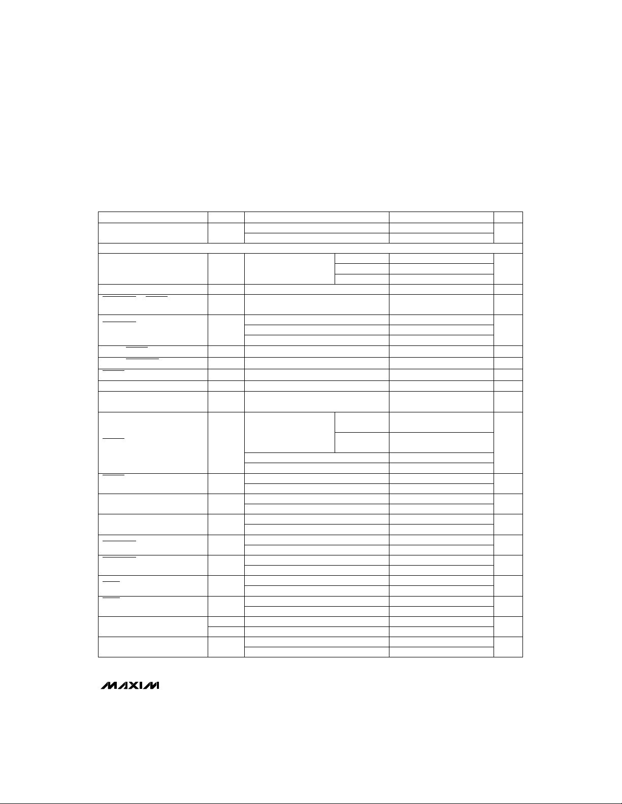
ELECTRICAL CHARACTERISTICS (continued)
(VCC= 4.60V to 5.5V for the MAX807L, VCC= 4.50V to 5.5V for the MAX807N, VCC= 4.35V to 5.5V for the MAX807M,
V
= 2.8V, V
BATT
BATT ON Output
Short-Circuit Current
RESET, LOW LINE, AND WATCHDOG TIMER
Reset Threshold VCCrising and falling
Reset Threshold Hysteresis
LOW LINE to RESET
Threshold Voltage
LOW LINE Threshold,
VCCRising
VCCto LOW LINE Delay VCCfalling at 1mV/µs 24 µs
RESET Active Timeout Period VCCrising
Watchdog Timeout Period
Minimum Watchdog Input
Pulse Width
RESET Output Voltage
RESET Output
Short-Circuit Current
RESET Output Voltage
RESET Output
Short-Circuit Current
LOW LINE Output Voltage
LOW LINE Output
Short-Circuit Current
WDO Output Voltage
WDO Output
Short-Circuit Current
WDI Threshold Voltage
(Note 4)
WDI Input Current
= 0V, TA= T
PFI
MIN
to T
. Typical values are tested with VCC= 5V and TA= +25°C, unless otherwise noted.)
MAX
CONDITIONS UNITSMIN TYP MAXSYMBOLPARAMETER
Sink current 70
Source current, VCC= 0V, V
RST
V
VCCfalling 30 52 70 mV
LR
V
LL
RP
t
WD
VIL= 0.8V, VIH= 0.75 x V
I
= 50µA,
SINK
V
= 0V, VCCfalling
BATT
= 3.2mA, VCC= 4.25V
SINK
I
= 0.1mA
SOURCE
I
SC
Output source current
= 3.2mA
SINK
I
= 5mA
SOURCE
I
SC
Output source current, VCC= 4.25V
= 3.2mA, VCC= 4.25V
SINK
I
= 5mA
SOURCE
I
SC
Output source current
= 3.2mA
SINK
I
= 5mA
SOURCE
I
SC
Output source current
V
IH
V
IL
V
IH
Reset deasserted, WDI = V
BATT
MAX807L
MAX807N
MAX807M
CC
VCC= 1V,
MAX807_C
VCC= 1.2V,
MAX807_E/M
CC
= 2.8V
4.600 4.675 4.750
4.500 4.575 4.650V
4.350 4.425 4.500
1.12 1.6 2.24 sec
100 ns
VCC- 1.5 VCC- 0.1
VCC- 1.5
VCC- 1.5
VCC- 1.5
0.75 x V
-50 -10Reset deasserted, WDI = 0V
5
13 mV
4.73 4.81MAX807L
4.63 4.71MAX807N
4.48 4.56MAX807M
0.1 0.4I
60Output sink current, VCC= 4.25V
1.6
60Output sink current
15
28Output sink current, VCC= 4.25V
20
35Output sink current
20
CC
16 50
0.3
0.3
0.4I
0.4I
0.4I
0.8
mA
V
V
µs26VCCto RESET Delay VCCfalling at 1mV/µs
ms140 200 280t
V
mA
V
mA
V
mA
V
mA
V
µA
MAX807L/M/N
_______________________________________________________________________________________ 3
Page 4
Full-Featured µP Supervisory Circuit with
±1.5% Reset Accuracy
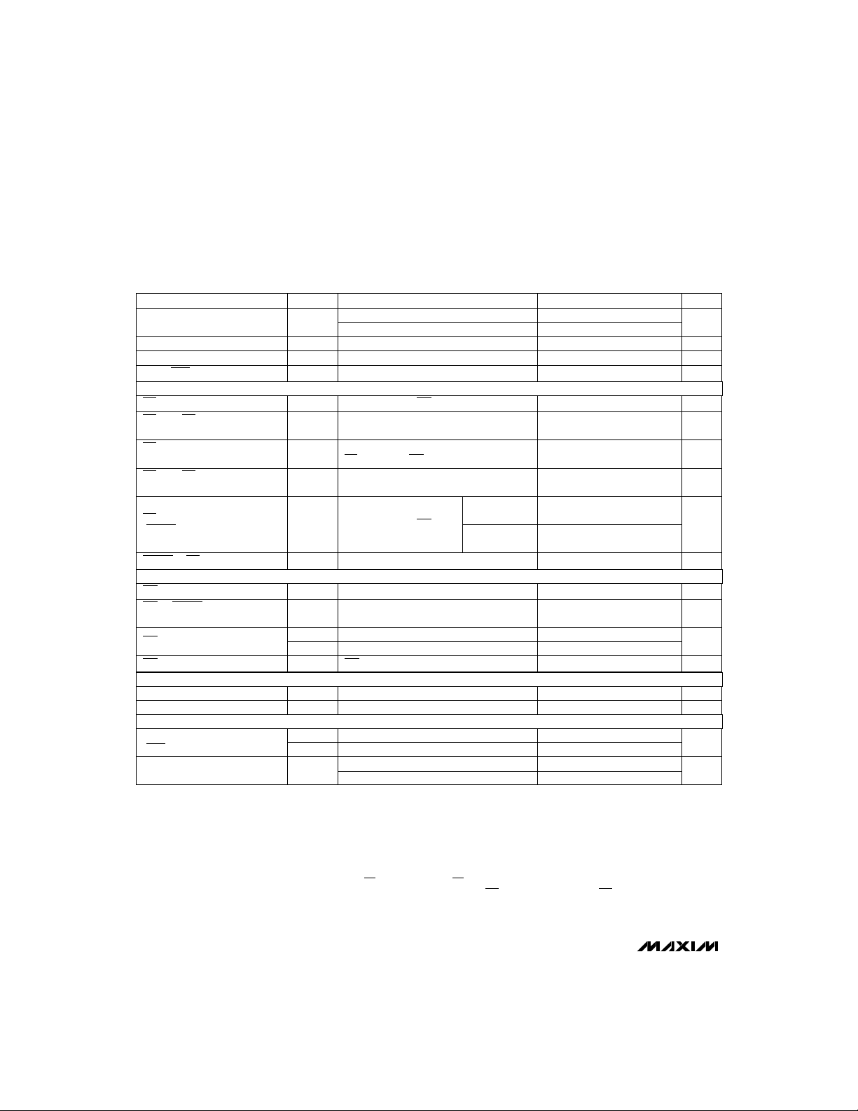
ELECTRICAL CHARACTERISTICS (continued)
(VCC= 4.60V to 5.5V for the MAX807L, VCC= 4.50V to 5.5V for the MAX807N, VCC= 4.35V to 5.5V for the MAX807M,
V
= 2.8V, V
BATT
PFI Input Threshold V
PFI Leakage Current ±0.005 ±40 nA
CHIP-ENABLE GATING
MAX807L/M/N
CE IN to CE OUT Resistance
(Note 6)
CE OUT Short-Circuit Current
(RESET active)
CE IN to CE OUT
Propagation Delay (Note 7)
CE OUT Output Voltage High
(RESET active)
RESET to CE OUT Delay VCCfalling 28 µs
MANUAL RESET INPUT
MR Minimum Pulse Input 1 µs
MR-to-RESET Propagation
Delay
MR Threshold
MR Pull-Up Current MR = 0V 50 100 200 µA
BATT OK COMPARATOR
BATT OK Threshold V
BATT OK Hysteresis 20 mV
LOGIC OUTPUTS
Output Voltage
(PFO, BATT OK)
Output Short-Circuit Current I
Note 1: Either VCCor V
Note 2: The supply current drawn by the MAX807 from the battery (excluding I
< V
Note 3: “+”= battery discharging current, “-”= battery charging current.
Note 4: WDI is internally connected to a voltage divider between V
disabling the watchdog function.
Note 5: Overdrive (V
Note 6: The chip-enable resistance is tested with V
Note 7: The chip-enable propagation delay is measured from the 50% point at CE
CC
= 0V, TA= T
PFI
BATT
< V
. In most applications, this is a brief period as VCCfalls through this region (see
BATT
) is measured from center of hysteresis band.
OD
to T
MIN
can go to 0V, if the other is greater than 2.0V.
. Typical values are tested with VCC= 5V and TA= +25°C, unless otherwise noted.)
MAX
CONDITIONS UNITSMIN TYP MAXSYMBOLPARAMETER
V
falling
PFI
PFT
V
rising
PFI
VOD= 30mV, V
Enabled mode, VCC= V
VCC= 5V, disabled mode,
CE OUT = 0V, MR = 0V
VCC= 5V, C
50Ω source impedance driver
Disabled mode, MR = 0V
V
IH
V
IL
BOK
V
OLISINK
V
OHISOURCE
SC
= 3.2mA 0.4
Output sink current 35
Output source current 20
CE IN
falling
PFI
RST
= 50pF,
LOAD
= 5mA VCC- 1.5
and GND. If unconnected, WDI is driven to 1.8V (typical),
CC
= VCC/2, and I
(max)
VCC= 5V,
I
OUT
VCC= 0V,
I
OUT
) typically goes to 15µA when (V
OUT
= 1mA.
CE IN
2.20 2.265 2.33
2.22 2.285 2.35
= 2mA
= 10µA
3.5
V
- 0.1 V
BATT
2.4
2.200 2.265 2.350 V
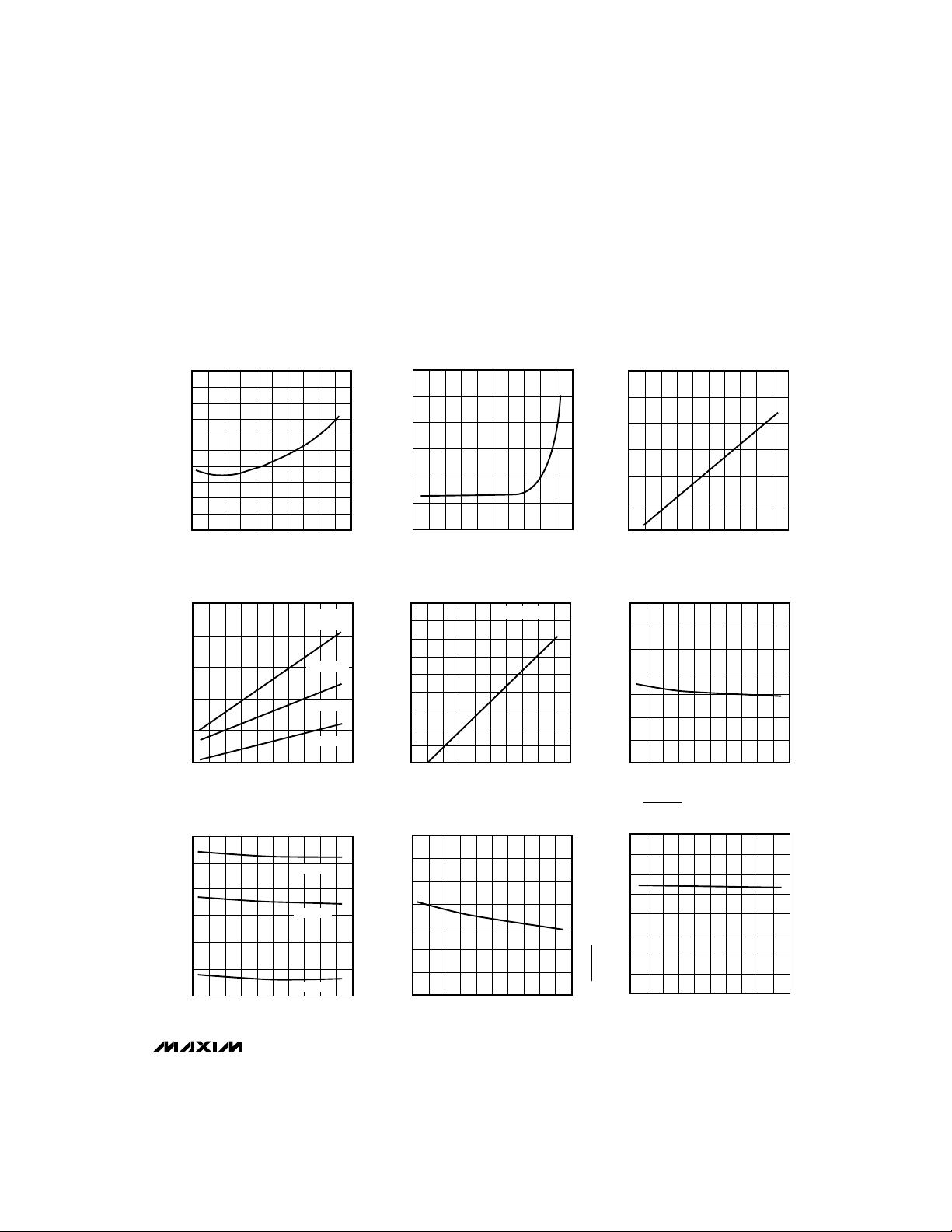
Typical Operating Characteristics
IN to the 50% point at CE OUT.
BATT
BATT
0.8
- 0.1V)
V
mV20PFI Hysteresis
µs14PFI to PFO Delay (Note 5)
µA±0.00002 ±1CE IN Leakage Current Disabled mode, MR = 0V
Ω75 150
mA17
ns28
V
ns170
V
V
mA
).
4 _______________________________________________________________________________________
Page 5
Full-Featured µP Supervisory Circuit with
±1.5% Reset Accuracy
__________________________________________Typical Operating Characteristics
(VCC= 5V, V
VCC SUPPLY CURRENT vs. TEMPERATURE
80
78
76
74
72
70
68
SUPPLY CURRENT (µA)
66
CC
V
64
62
60
-60 -20 60 140
30
25
20
15
10
BATT-to-OUT ON-RESISTANCE (Ω)
5
-60 -20 60 140
4.70
4.65
4.60
4.55
4.50
RESET THRESHOLD (V)
4.45
4.40
-60 -20 60 140
= 2.8V, PFI = 0V, no load, TA= +25°C, unless otherwise noted.)
BATT
BATTERY SUPPLY CURRENT vs.
(NORMAL OPERATING MODE)
20 100-40 40 120080
TEMPERATURE (°C)
BATT-to-OUT ON-RESISTANCE
vs. TEMPERATURE
V
CC
I
OUT
V
BATT
V
BATT
V
BATT
20 100-40 40 120080
TEMPERATURE (°C)
RESET THRESHOLD
vs. TEMPERATURE
MAX807L
MAX807N
MAX807M
20 100-40 40 120080
TEMPERATURE (°C)
= 0V
= 10mA
= 2.0V
= 2.8V
= 4.5V
MAX807-01
MAX807-04
MAX807-07
TEMPERATURE (BATTERY-BACKUP MODE)
3.0
2.5
2.0
1.5
1.0
0.5
BATTERY SUPPLY CURRENT (µA)
0
-60 -20 60 140
1.6
1.5
1.4
1.3
1.2
1.1
1.0
-to-OUT ON-RESISTANCE (Ω)
0.9
CC
V
0.8
0.7
-60 -20 60 140
vs. TEMPERATURE (V
280
260
240
220
200
180
RESET TIMEOUT PERIOD (ms)
160
140
-60 -20 60 140
20 100-40 40 120080
TEMPERATURE (°C)
VCC-to-OUT ON-RESISTANCE
vs. TEMPERATURE
20 100-40 40 120080
TEMPERATURE (°C)
RESET TIMEOUT PERIOD
20 100-40 40 120080
TEMPERATURE (°C)
I
= 250mA
OUT
RISING)
CC
CHIP-ENABLE PROPAGATION DELAY
6
MAX807-02
5
4
3
2
PROPAGATION DELAY (ns)
1
0
2.340
MAX807-05
2.320
2.300
2.280
2.260
PFI THRESHOLD (V)
2.240
2.220
2.200
80
MAX807-08
70
60
50
40
30
20
10
LOW LINE-to-RESET THRESHOLD (mV)
0
vs. TEMPERATURE
-60 -20 60 140
vs. TEMPERATURE (V
-60 -20 60 140
vs. TEMPERATURE (V
-60 -20 60 140
20 100-40 40 120080
TEMPERATURE (°C)
PFI THRESHOLD
20 100-40 40 120080
TEMPERATURE (°C)
LOW LINE -to-RESET THRESHOLD
20 100-40 40 120080
TEMPERATURE (°C)
PFI
CC
FALLING)
FALLING)
MAX807L/M/N
MAX807-03
MAX807-06
MAX807-09
_______________________________________________________________________________________
5
Page 6

Full-Featured µP Supervisory Circuit with
±1.5% Reset Accuracy
____________________________Typical Operating Characteristics (continued)
(VCC= 5V, V
= 2.8V, PFI = 0V, no load, TA= +25°C, unless otherwise noted.)
BATT
LOW LINE THRESHOLD
vs. TEMPERATURE (V
4.80
4.75
4.70
4.65
4.60
MAX807L/M/N
4.55
4.50
LOW LINE THRESHOLD (V)
4.45
4.40
-60 -20 60 140
16
14
12
10
8
6
4
BATTERY CURRENT (µA)
2
0
2.5 2.6 2.7 2.8 2.9 3.0
TEMPERATURE (°C)
BATTERY CURRENT
vs. INPUT SUPPLY VOLTAGE
1000
CC
“L” VERSION
“N” VERSION
“M” VERSION
20 100-40 40 120080
VCC (V)
RISING)
MAX807-10
MAX807-13
VCC-to-OUT vs.
OUTPUT CURRENT
LOW LINE COMPARATOR PROPAGATION
DELAY vs. TEMPERATURE (V
40
35
V
FALLING AT 1mV/µs
CC
30
25
20
15
10
5
LOW LINE COMPARATOR PROP. DELAY (µs)
0
-60 -20 60 140
CHIP-ENABLE PROPAGATION DELAY
8
6
4
2
PROPAGATION DELAY (ns)
0
0 50 100
20 100-40 40 120080
TEMPERATURE (°C)
vs. CE OUT LOAD CAPACITANCE
50Ω DRIVER
C
(pF)
LOAD
MAX807-16
FALLING)
CC
MAX807-11
MAX807-14
MAXIMUM TRANSIENT DURATION vs.
RESET COMPARATOR OVERDRIVE
1000
RESET COMPARATOR PROPAGATION
DELAY vs. TEMPERATURE (V
40
35
30
25
20
15
10
5
RESET COMPARATOR PROP. DELAY (µs)
0
-60 -20 60 140
1000
100
BATT-to-OUT (mV)
10
1 10 100
V
FALLING AT 1mV/µs
CC
TEMPERATURE (°C)
BATT-to-OUT vs.
OUTPUT CURRENT
V
= 0V
CC
SLOPE = 12Ω
FALLING)
CC
20 100-40 40 120080
I
(mA)
OUT
MAX807-17
MAX807-12
MAX807-15
100
-VOUT (mV)
CC
V
10
1
1 10010 1000
SLOPE = 1.0Ω
I
(mA)
OUT
100
10
MAXIMUM TRANSIENT DURATION (µs)
1
1 10010 1000
RESET COMPARATOR OVERDRIVE (mV)
RESET OCCURS
6 _______________________________________________________________________________________
Page 7

Full-Featured µP Supervisory Circuit with
±1.5% Reset Accuracy
______________________________________________________________Pin Description
PIN
Power-Fail Input. When PFI is less than V
PFO2
3
CC
WDI4
MR6
LOW LINE7
RESET8
RESET9
WDO10
CE OUT11
BATT ON13
BATT14
BATT OK15
OUT16
Power-Fail Output. This CMOS-logic output goes low when PFI is less than V
V
≥ 4V. PFO swings between VCCand GND.
CC
Input Supply Voltage, nominally +5V. Bypass with a 0.1µF capacitor to GND.V
Watchdog Input. If WDI remains high or low longer than the the watchdog timeout period (1.6sec
typical), WDO goes low. Leave unconnected to disable the watchdog function.
GroundGND5
Manual-Reset Input. A logic low on MR asserts reset. Reset remains asserted as long as MR remains low
and for 200ms after MR returns high. MR is an active-low input with an internal pull-up to VCC. It can be
driven using TTL or CMOS logic, or shorted to ground with a switch. Connect to VCC, or leave unconnected if not used.
Low-Line Comparator Output. This CMOS-logic output goes low when VCCfalls to 52mV above the reset
threshold. Use this output to generate an NMI to initiate an orderly shutdown routine when VCCis falling.
LOW LINE swings between VCCand GND.
Active-High Reset Output. RESET is the inverse of RESET. It is a CMOS output that sources and sinks
current. RESET swings between VCCand GND.
Active-Low Reset Output. RESET is triggered and stays low when VCCis below the reset threshold or
when MR is low. It remains low 200ms after VCCrises above the reset threshold or MR returns high.
RESET has a strong pull-down but a relatively weak pull-up, and can be wire-OR connected to logic
gates. Valid for VCC≥ 1V. RESET swings between VCCand GND.
Watchdog Output. This CMOS-logic output goes low if WDI remains high or low longer than the watchdog timeout period (tWD), and remains low until the next transition of WDI. WDO remains high if WDI is
unconnected. WDO is high during reset. WDO swings between VCCand GND. Connect WDO to MR to
generate resets during watchdog faults.
Chip-Enable Output. Output to the chip-enable gating circuit. CE OUT is pulled up to the higher of V
or V
, when the chip-enable gate is disabled.
BATT
Chip-Enable InputCE IN12
Battery On Output. CMOS-logic output/external bypass switch driver. High when OUT is connected to
BATT and low when OUT is connected to VCC. Connect the base of a PNP transistor or gate of a PMOS
transistor to BATT ON for I
VCCand V
Backup-Battery Input. When VCCfalls below the reset threshold and V
BATT. V
BATT is bypassed with a 0.1µF capacitor to GND. If no battery is used, connect BATT to ground, and
connect VCCand OUT together.
Battery OK Signal Output. High in normal operating mode when V
VCC≥ 4V.
Output Supply Voltage to CMOS RAM. When VCCexceeds the reset threshold or VCC> V
connected to VCC. When VCCfalls below the reset threshold and V
OUT with a 0.1µF capacitor to GND.
, and GND.
BATT
may exceed VCC. The battery can be removed while the MAX807 is powered-up, provided
BATT
requirements exceeding 250mA. BATT ON swings between the higher of
OUT
PFT
FUNCTIONNAME
(2.265V), PFO goes low. Connect to ground when unused.PFI1
(2.265V). Valid for
PFT
CC
, OUT switches from VCCto
BATT
exceeds V
BATT
, OUT connects to BATT. Bypass
BATT
(2.265V). Valid for
BOK
BATT
, OUT is
MAX807L/M/N
_______________________________________________________________________________________ 7
Page 8

Full-Featured µP Supervisory Circuit with
±1.5% Reset Accuracy
_______________Detailed Description
The MAX807 microprocessor (µP) supervisory circuit
provides power-supply monitoring, backup-battery
switchover, and program execution watchdog functions
in µP systems (Figure 1). Use of BiCMOS technology
results in an improved 1.5% reset-threshold precision,
while keeping supply currents typically below 70µA.
The MAX807 is intended for battery-powered applications that require high reset-threshold precision, allowing a wide power-supply operating range while
preventing the system from operating below its specified voltage range.
MAX807L/M/N
V
CC
BATT
GND
PFI
BATTERY-BACKUP
COMPARATOR
RESET
COMPARATOR
LOW-LINE
COMPARATOR
BATTERY-OK
COMPARATOR
POWER-FAIL
COMPARATOR
2.275V
OSCILLATOR
The MAX807’s RESET output ensures that the µP pow-
RESET and RESET Outputs
ers up in a known state, and prevents code execution
errors during power-down and brownout conditions. It
accomplishes this by resetting the µP, terminating program execution when VCCdips below the reset threshold or MR is pulled low. Each time RESET is asserted it
stays low for the 200ms reset timeout period, which is
set by an internal timer to ensure the µP has adequate
time to return to an initial state. Any time VCCgoes
below the reset threshold before the reset timeout period is completed, the internal timer restarts. The watchdog timer can also initiate a reset if WDO is connected
to MR. See the
WATCHDOG
TRANSITION
DETECTOR
STATE
MACHINE
Watchdog Input
P
N
V
CC
50kΩ
THE HIGHER
OF V
OR V
CC
BATT
section.
OUT
BATT ON
LOW LINE
BATT OK
PFO
WDI
MR
RESET
RESET
WDO
MAX807
P
CE IN
N
P
CE OUT
Figure 1. Block Diagram
8 _______________________________________________________________________________________
Page 9

Full-Featured µP Supervisory Circuit with
±1.5% Reset Accuracy
V
V
V
RSTVLL
RST
+ V
RST
LR
MAX807L/M/N
V
LOW LINE
V
V
V
CE OUT
V
RESET
RESET
CC
V
BATT
SHOWN FOR V
= 0V to 5V, V
CC
t
RP
t
RP
= 2.8V, CE IN = GND
BATT
V
LOW LINE
V
V
V
CE OUT
V
RESET
RESET
CC
SHOWN FOR V
= 5V to 0V, V
CC
V
BATT
= 2.8V, CE IN = GND
BATT
Figure 2a. Timing Diagram, VCCRising Figure 2b. Timing Diagram, VCCFalling
The RESET output is active low and implemented with a
strong pull-down/relatively weak pull-up structure. It is
guaranteed to be a logic low for 0V < VCC< V
vided V
is greater than 2V. Without a backup bat-
BATT
RST
, pro-
MANUAL RESET
tery, RESET is guaranteed valid for VCC≥ 1. It typically
sinks 3.2mA at 0.1V saturation voltage in its active state.
The RESET output is the inverse of the RESET output; it
both sources and sinks current and cannot be wire-OR
connected.
OTHER
RESET
SOURCES
*
*
Manual Reset Input
Many µP-based products require manual-reset capability to allow an operator or test technician to initiate a
* DIODES NOT REQUIRED ON OPEN-DRAIN OUTPUTS
reset. The Manual Reset (MR) input permits the generation of a reset in response to a logic low from a switch,
WDO, or external circuitry. Reset remains asserted
while MR is low, and for 200ms after MR returns high.
Figure 3. Diode “OR” connections allow multiple reset sources
to connect to MR
.
MR has an internal 50µA to 200µA pull-up current, so it
can be left open if it is not used. MR can be driven with
TTL or CMOS-logic levels, or with open-drain/collector
outputs. Connect a normally open momentary switch
from MR to GND to create a manual-reset function;
external debounce circuitry is not required. If MR is driven from long cables or if the device is used in a noisy
environment, connect a 0.1µF capacitor from MR to
ground to provide additional noise immunity. As shown
in Figure 3, diode-ORed connections can be used to
allow manual resets from multiple sources. Figure 4
shows the reset timing.
The watchdog circuit monitors the µP’s activity. If the
µP does not toggle the watchdog input (WDI) within
1.6sec, WDO goes low. The internal 1.6sec timer is
cleared and WDO returns high when reset is asserted
or when a transition (low-to-high or high-to-low) occurs
at WDI while RESET is high. As long as reset is asserted, the timer remains cleared and does not count. As
soon as reset is released, the timer starts counting
(Figure 5). Supply current is typically reduced by 10µA
when WDI is at a valid logic level.
MR
MAX807
Watchdog Timer
Watchdog Input
_______________________________________________________________________________________ 9
Page 10

Full-Featured µP Supervisory Circuit with
±1.5% Reset Accuracy
MR
RESET
CE IN
0V
CE OUT
Figure 4. Manual-Reset Timing Diagram
MAX807L/M/N
1µs MIN
170ns
28µs TYP
Watchdog Output
WDO remains high if there is a transition or pulse at
WDI during the watchdog timeout period. WDO goes
low if no transition occurs at WDI during the watchdog
timeout period. The watchdog function is disabled and
WDO is a logic high when VCCis below the reset
threshold or WDI is an open circuit. To generate a system reset on every watchdog fault, simply diode-OR
connect WDO to MR (Figure 6). When a watchdog fault
occurs in this mode, WDO goes low, which pulls MR
low, causing a reset pulse to be issued. As soon as
reset is asserted, the watchdog timer clears and WDO
returns high. With WDO connected to MR, a continuous
high or low on WDI will cause 200ms reset pulses to be
issued every 1.6sec.
The MAX807 provides internal gating of chip-enable
Chip-Enable Signal Gating
(CE) signals to prevent erroneous data from corrupting
the CMOS RAM in the event of a power failure. During
normal operation, the CE gate is enabled and passes
all CE transitions. When reset is asserted, this path
becomes disabled, preventing erroneous data from
corrupting the CMOS RAM. The MAX807 uses a series
transmission gate from the Chip-Enable Input (CE IN) to
the Chip-Enable Output (CE OUT) (Figure 1).
The 8ns max chip-enable propagation from CEIN to CE
OUT enables the MAX807 to be used with most µPs.
Chip-Enable Input
CE IN is high impedance (disabled mode) while RESET
is asserted. During a power-down sequence when V
CC
passes the reset threshold, the CE transmission gate
disables and CE IN becomes high impedance 28µs
after reset is asserted (Figure 7). During a power-up
sequence, CE IN remains high impedance (regardless
of CE IN activity) until reset is deasserted following the
reset-timeout period.
In the high-impedance mode, the leakage currents into
this input are ±1µA max over temperature. In the lowimpedance mode, the impedance of CE IN appears as
a 75Ω resistor in series with the load at CE OUT.
The propagation delay through the CE transmission
gate depends on both the source impedance of the
drive to CE IN and the capacitive loading on CE OUT
V
RST
V
CC
t
RESET
WDO
WDI
WDO CONNECTED TO µP INTERRUPT
Figure 5. Watchdog Timing Relationship
10 ______________________________________________________________________________________
RP
V
CC
t
WD
WDO
t
RESET
WDI
Figure 6. Generating a Reset on Each Watchdog Fault
RP
WDO
MR
t
WD
V
CC
MAX807
RESET
∼50µs
t
RP
4.7k
TO µP
Page 11

Full-Featured µP Supervisory Circuit with
±1.5% Reset Accuracy
V
MAX
CE IN
LOAD
RST
V
CC
MAX807
GND
V
CC
MAX807
x t
SHDN
CE OUT
LOW LINE
GND
) / VLR(min)
V
CC
RESET
THRESHOLD
CE IN
CE OUT
RESET
RESET
Figure 7. Reset and Chip-Enable Timing Figure 8. CE Propagation Delay Test Circuit
28µs
26µs
26µs
50Ω DRIVER
(see the Chip-Enable Propagation Delay vs. CE OUT
Load Capacitance graph in the
Characteristics
). The CE propagation delay is produc-
Typical Operating
tion tested from the 50% point on CE IN to the 50%
point on CE OUT using a 50Ω driver and 50pF of load
capacitance (Figure 8). For minimum propagation
delay, minimize the capacitive load at CE OUT and use
a low output-impedance driver.
REGULATOR
4.5V to 5.5V
C
HOLD
Chip-Enable Output
In the enabled mode, the impedance of CEOUT is equivalent to 75Ω in series with the source driving CE IN. In the
disabled mode, the 75Ω transmission gate is off and CE
OUT is actively pulled to the higher of VCCor V
BATT
. This
source turns off when the transmission gate is enabled.
C
> I
HOLD
LOAD
V
x t
SHDN
LR
Low-Line Comparator
The low-line comparator monitors VCCwith a threshold
voltage typically 52mV above the reset threshold, with
13mV of hysteresis. Use LOW LINE to provide a nonmaskable interrupt (NMI) to the µP when power begins
to fall, to initiate an orderly software shutdown routine.
In most battery-operated portable systems, reserve
energy in the battery provides ample time to complete
the shutdown routine once the low-line warning is
encountered, and before reset asserts. If the system
must contend with a more rapid VCCfall time—such as
when the main battery is disconnected, a DC-DC converter shuts down, or a high-side switch is opened during normal operation—use capacitance on the VCCline
to provide time to execute the shutdown routine (Figure
9). First calculate the worst-case time required for the
system to perform its shutdown routine. Then, with the
Figure 9. Using LOW LINE to Provide a Power-Fail Warning to
the µP
worst-case shutdown time, the worst-case load current,
and the minimum low-line to reset threshold (V
calculate the amount of capacitance required to allow the
shutdown routine to complete before reset is asserted:
C
= (I
HOLD
where t
is the time required for the system to com-
SHDN
plete the shutdown routine, and includes the VCCto
low-line propagation delay; and where I
rent being drained from the capacitor, VLRis the lowline to reset threshold.
LOAD
50pF
C
LOAD
TO µP NMI
LR(min)
is the cur-
MAX807L/M/N
),
______________________________________________________________________________________ 11
Page 12

Full-Featured µP Supervisory Circuit with
±1.5% Reset Accuracy
V
IN
V
R1
R2
V
IN
V
CC
PFO
MAX807L/M/N
1
V
= R2
(V
TRIP
V
+ V
PFT
= R2
(V
)
L
PFT
+
)
PFH
(
R1
1
1
+
(
)
R2
R1
CC
MAX807
PFI PFO
GND
V
V
TRIP
L
1
V
CC
–
)
R2
R1
V
CC
–
R1
WHERE
NOTE: V
0V
V
PFT
V
PFH
TRIP, VL
V
IN
= 2.265V
= 20mV
ARE NEGATIVE
R1
R2
V
CC
PFO
R2
R1
+
V
V
=
TRIP
PFT
(
)
R2
R2
R1
VH = (V
b)a)
PFT + VPFH
+
)
(
R2
Figure 10. Using the Power-Fail Comparator to Monitor an Additional Power Supply: a) VINis Negative, b) VINis Positive
FROM
REGULATED
SUPPLY
0.1µF
a)
CC
MAX807
LOW LINE
GND
OUTV
BATT
RESET
WDI
0.1µF
2.8V
µP POWER
POWER TO
CMOS RAM
µP
RESET
NMI
I/O LINE
PFI is the noninverting input to an uncommitted comparator. If PFI is less than V
The power-fail comparator is intended to monitor the
preregulated input of the power supply, providing an
early power-fail warning so software can conduct an
orderly shutdown. It can also be used to monitor supplies other than 5V. Set the power-fail threshold with a
resistor divider, as shown in Figure 10.
PFI is the input to the power-fail comparator. The typical
comparator delay is 14µs from VILto VOL(power failing),
and 32µs from VIHto VOH(power being restored). If
unused, connect this input to ground.
VOLTAGE
REGULATOR
0.1µF
CC
PFI
MAX807
GND
OUTV
BATT
RESET
PFO
WDI
0.1µF
2.8V
µP POWER
POWER TO
CMOS RAM
µP
RESET
NMI
I/O LINE
The Power-Fail Output (PFO) goes low when PFI goes
below V
. It typically sinks 3.2mA with a saturation
PFT
voltage of 0.1V. With PFI above V
pulled to VCC. Connecting PFI through a voltage divider
to a preregulated supply allows PFO to generate an
NMI as the preregulated power begins to fall (Figure
11b). If the preregulated supply is inaccessible, use
LOW LINE to generate the NMI (Figure 11a). The LOW
LINE threshold is typically 52mV above the reset
threshold (see
Low-Line Comparator
V
CC
MAX807
PFI PFO
GND
V
TRIPVH
)
Power-Fail Comparator
(2.265V), PFO goes low.
PFT
MR
V
Power-Fail Input
Power-Fail Output
, PFO is actively
PFT
section).
IN
b)
Figure 11. a) If the preregulated supply is inaccessible, LOW
LINE generates the NMI for the µP. b) Use PFO to generate the
µP NMI if the preregulated supply is accessible.
12 ______________________________________________________________________________________
Page 13

Full-Featured µP Supervisory Circuit with
±1.5% Reset Accuracy
Table 1. Input and Output Status in Battery-Backup Mode
PIN
The power-fail comparator remains active in battery-backup mode for VCC≥ 4V.PFI1
The power-fail comparator remains active in battery-backup mode for VCC≥ 4V. Below 4V, PFO is forced low.PFO2
3
V
CC
BATT
Figure 12. VCCand BATT-to-OUT Switch
CC
CONTROL
CIRCUITRY
Battery switchover comparator monitors VCCfor active switchover.V
WDI is ignored and goes high impedance.WDI4
Ground—0V reference for all signals.GND5
MR is ignored.MR6
Logic low.LOW LINE7
Logic high; the open-circuit output voltage is equal to VCC.RESET8
Logic low.RESET9
Logic high. The open-circuit output voltage is equal to VCC.WDO10
Logic high. The open-circuit output voltage is equal to V
High impedance.CE IN12
Logic high. The open-circuit output voltage is equal to V
Supply current is 1µA maximum for V
Logic high when V
OUT is connected to BATT through two internal PMOS switches in series.OUT16
MAX807
P
PP
BATT
exceeds 2.285V. Valid for VCC≥ 4V. Below 4V, BATT OK is forced low.BATT OK15
OUT
0.1µF
Battery-Backup Mode
Battery backup preserves the contents of RAM in the
event of a brownout or power failure. With a backup
battery installed at BATT, the MAX807 automatically
switches RAM to backup power when VCCfalls. Two
conditions are required for switchover to battery-backup mode: 1) VCCmust be below the reset threshold; 2)
VCCmust be below V
. Table 1 lists the status of
BATT
inputs and outputs during battery-backup mode.
FUNCTIONNAME
BATT
BATT
BATT
≤ 2.8V.BATT14
The BATT input is similar to VCC, except the PMOS
switch is much smaller. This input is designed to conduct up to 20mA to OUT during battery backup. The
on-resistance of the PMOS switch is approximately
13Ω. Figure 12 shows the two series pass elements
between the BATT input and OUT that facilitates UL
approval. V
BATT
tion without causing a reset.
The output supply (OUT) transfers power from VCCor
BATT to the µP, RAM, and other external circuitry. At
the maximum source current of 250mA, V
cally be 260mV below VCC. Decouple this terminal with
a 0.1µF capacitor.
The battery on (BATT ON) output indicates the status of
the internal battery switchover comparator, which controls the internal VCCand BATT switches. For V
greater than V
effect), BATT ON typically sinks 3.2mA at 0.4V. In battery-backup mode, this output sources approximately
5mA. Use BATT ON to indicate battery switchover status, or to supply gate or base drive for an external pass
transistor for higher current applications (see
Operating Circuit
.CE OUT11
.BATT ON13
Backup-Battery Input
can exceed VCCduring normal opera-
Output Supply Voltage
will typi-
OUT
BATT ON Output
(ignoring the small hysteresis
BATT
Typical
).
MAX807L/M/N
CC
______________________________________________________________________________________ 13
Page 14
Full-Featured µP Supervisory Circuit with
±1.5% Reset Accuracy
The BATT OK comparator monitors the backup battery
BATT OK Output
voltage, comparing it with a 2.265V reference (VCC≥
4V). BATT OK remains high as long as the backup battery voltage remains above 2.265V, signaling that the
backup battery has sufficient voltage to maintain the
memory of static RAM. When the battery voltage drops
below 2.265V, the BATT OK output drops low, signaling
that the backup battery needs to be changed.
__________Applications Information
The MAX807 is not short-circuit protected. Shorting
OUT to ground, other than power-up transients such as
MAX807L/M/N
charging a decoupling capacitor, may destroy the
device. If long leads connect to the IC’s inputs, ensure
that these lines are free from ringing and other conditions that would forward bias the IC’s protection diodes.
There are two distinct modes of operation:
1) Normal Operating Mode, with all circuitry powered
up. Typical supply current from VCCis 70µA, while
only leakage currents flow from the battery.
2) Battery-Backup Mode, where VCCis below V
and V
ically less than 1µA.
BATT has the same operating voltage range as VCC, and
the battery-switchover threshold voltage is typically
V
BATT
VCCis increasing. This hysteresis allows use of a
. The supply current from the battery is typ-
RST
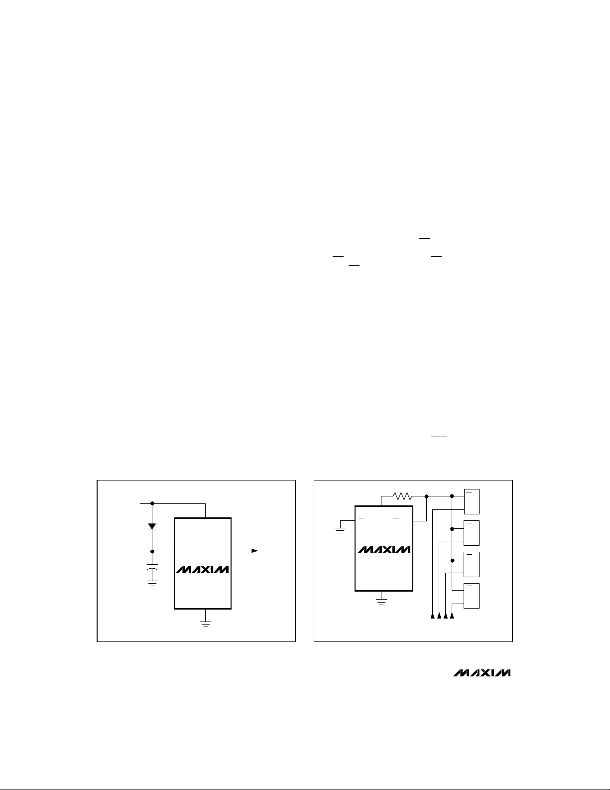
Using SuperCaps™ or
MaxCaps™ with the MAX807
when VCCis decreasing or V
BATT
+ 0.06V when
BATT
SuperCap (e.g., order of 0.47F) and a simple charging
circuit as a backup source (Figure 13). Since V
BATT
can
exceed VCCwhile VCCis above the reset threshold,
there are no special precautions when using these µP
supervisors with a SuperCap.
Alternative Chip-Enable Gating
Using memory devices with CE and CE inputs allows
the MAX807 CE loop to be bypassed. To do this, connect CE IN to ground, pull up CE OUT to OUT, and
connect CE OUT to the CE input of each memory
device (Figure 14). The CE input of each part then connects directly to the chip-select logic, which does not
have to be gated by the MAX807.
Adding Hysteresis to the
Power-Fail Comparator
The power-fail comparator has a typical input hysteresis of 20mV. This is sufficient for most applications
where a power-supply line is being monitored through
an external voltage divider (Figure 10).
Figure 15 shows how to add hysteresis to the power-fail
comparator. Select the ratio of R1 and R2 such that PFI
sees 2.265V when VINfalls to the desired trip point
(V
). Resistor R3 adds hysteresis. It will typically be
TRIP
an order of magnitude greater than R1 or R2. The current through R1 and R2 should be at least 1µA to
ensure that the 25nA (max) PFI input current does not
shift the trip point. R3 should be larger than 10kΩ to
prevent it from loading down the PFO pin. Capacitor C1
adds additional noise rejection.
Rp*
+5V
V
1N4148
0.47F
Figure 13. SuperCap or MaxCap on BATT
14 ______________________________________________________________________________________
CC
BATT OUT
MAX807
GND
*MAXIMUM Rp VALUE DEPENDS ON
THE NUMBER OF RAMS.
MINIMUM Rp VALUE IS 1kΩ
Figure 14. Alternate CE Gating
CE IN
OUT
MAX807
GND
CE OUT
ACTIVE-HIGH CE
LINES FROM LOGIC
CE
RAM 1
CE
CE
RAM 2
CE
CE
RAM 3
CE
CE
RAM 4
CE
Page 15

Full-Featured µP Supervisory Circuit with
±1.5% Reset Accuracy
The backup battery may be disconnected while VCCis
Backup-Battery Replacement
above the reset threshold, provided BATT is bypassed
with a 0.1µF capacitor to ground. No precautions are
necessary to avoid spurious reset pulses.
Negative-Going VCCTransients
While issuing resets to the µP during power-up, powerdown, and brownout conditions, these supervisors are
relatively immune to short-duration negative-going V
CC
transients (glitches). It is usually undesirable to reset
the µP when VCCexperiences only small glitches.
The
Typical Operating Characteristics
show Maximum
Transient Duration vs. Reset Comparator Overdrive, for
which reset pulses are not generated. The graph was
produced using negative-going VCCpulses, starting at
5V and ending below the reset threshold by the magnitude indicated (reset comparator overdrive). The graph
shows the maximum pulse width that a negative-going
VCCtransient may typically have without causing a
reset pulse to be issued. As the amplitude of the transient increases (i.e., goes farther below the reset
threshold), the maximum allowable pulse width
decreases.
Typically, a VCCtransient that goes 40mV below the
reset threshold and lasts for 3µs or less will not cause a
reset pulse to be issued.
V
IN
R1
C1*
R3
R2
TO µP
+5V
PFO
0V
0V
Figure 15. Adding Hysteresis to the Power-Fail Comparator
R1 + R2
= 2.265
V
TRIP
R2
= 2.265 /
V
H
R1 + R2
R2
|| R3
V
R3 R1 R3 R2
||
+5V
V
CC
PFI
MAX807
PFO
GND
VL
V
HVTRIP
V
IN
- 2.265 + 5 - 2.265 = 2.265
L
*OPTIONAL
START
SET
WDI
LOW
SUBROUTINE
OR PROGRAM LOOP,
SET WDI
HIGH
RETURN
END
Figure 16. Watchdog Flow Diagram
A 0.1µF bypass capacitor mounted close to the V
CC
pin provides additional transient immunity.
Watchdog Software Considerations
To help the watchdog timer keep a closer watch on software execution, you can use the method of setting and
resetting the watchdog input at different points in the
program, rather than “pulsing” the watchdog input highlow-high or low-high-low. This technique avoids a “stuck”
loop where the watchdog timer continues to be reset
within the loop, keeping the watchdog from timing out.
Figure 16 shows an example flow diagram where the
I/O driving the watchdog input is set high at the beginning of the program, set low at the beginning of every
subroutine or loop, then set high again when the program returns to the beginning. If the program should
“hang” in any subroutine, the I/O is continually set low
and the watchdog timer is allowed to time out, causing
a reset or interrupt to be issued.
Maximum VCCFall Time
The VCCfall time is limited by the propagation delay of
the battery switchover comparator and should not
exceed 0.03V/µs. A standard rule for filter capacitance
on most regulators is on the order of 100µF per amp of
current. When the power supply is shut off or the main
battery is disconnected, the associated initial VCCfall
rate is just the inverse or 1A / 100µF = 0.01V/µs. The
VCCfall rate decreases with time as VCCfalls exponentially, which more than satisfies the maximum fall-time
requirement.
MAX807L/M/N
______________________________________________________________________________________ 15
Page 16

Full-Featured µP Supervisory Circuit with
±1.5% Reset Accuracy
__________Typical Operating Circuit
+5V
0.1µF
BATT
V
CC
ON
™
+12V
BATT
MR
PFI
MAX807
LOW LINE
GND
CE OUT
CE IN
RESET RESET
RESET
BATT OK
WDO
0.47F*
OTHER
SYSTEM
RESET
MAX807L/M/N
SOURCES
PUSH-
BUTTON
SWITCH
SUPPLY
*
MaxCap
OUT
WDI
PFO
0.1µF
ADDRESS
DECODE
CMOS
RAM
A0–A15
I/O
NMI
RESET
INTERRUPT
+12V SUPPLY FAILURE
WATCHDOG FAILURE
___________________Chip Information
______________Ordering Information
†
PART
0°C to +70°C
-40°C to +85°C
-55°C to +125°CMAX807_MJE
REAL-
TIME
CLOCK
MAX807_CPE
MAX807_EWE
†
This part offers a choice of reset threshold voltage. From the
table below, select the suffix corresponding to the desired
threshold and insert it into the blank to complete the part number.
SUFFIX
µP
L
N
RESET THRESHOLD (V)
MIN
4.60
4.50
4.675
4.575 4.65
4.425 4.504.35M
TYP
PIN-PACKAGETEMP. RANGE
16 Plastic DIP
16 Wide SO0°C to +70°CMAX807_CWE
16 Plastic DIP-40°C to +85°CMAX807_EPE
16 Wide SO
16 CERDIP
MAX
4.75
TRANSISTOR COUNT: 984
Maxim cannot assume responsibility for use of any circuitry other than circuitry entirely embodied in a Maxim product. No circuit patent licenses are
Maxim cannot assume responsibility for use of any circuitry other than circuitry entirely embodied in a Maxim product. No circuit patent licenses are
Maxim cannot assume responsibility for use of any circuitry other than circuitry entirely embodied in a Maxim product. No circuit patent licenses are
Maxim cannot assume responsibility for use of any circuitry other than circuitry entirely embodied in a Maxim product. No circuit patent licenses are
implied. Maxim reserves the right to change the circuitry and specifications without notice at any time.
implied. Maxim reserves the right to change the circuitry and specifications without notice at any time.
implied. Maxim reserves the right to change the circuitry and specifications without notice at any time.
implied. Maxim reserves the right to change the circuitry and specifications without notice at any time.
16
__________________Maxim Integrated Products, 120 San Gabriel Drive, Sunnyvale, CA 94086 (408) 737-7600
16
__________________Maxim Integrated Products, 120 San Gabriel Drive, Sunnyvale, CA 94086 (408) 737-7600
16
__________________Maxim Integrated Products, 120 San Gabriel Drive, Sunnyvale, CA 94086 (408) 737-7600
16
__________________Maxim Integrated Products, 120 San Gabriel Drive, Sunnyvale, CA 94086 (408) 737-7600
© 1995 Maxim Integrated Products Printed USA is a registered trademark of Maxim Integrated Products.
© 1995 Maxim Integrated Products Printed USA is a registered trademark of Maxim Integrated Products.
© 1995 Maxim Integrated Products Printed USA is a registered trademark of Maxim Integrated Products.
© 1995 Maxim Integrated Products Printed USA is a registered trademark of Maxim Integrated Products.
 Loading...