19-0243; Rev 1; 9/94
3.0V/3.3V Microprocessor Supervisory Circuits
_______________General Description
These microprocessor (µP) supervisory circuits reduce
the complexity and number of components required for
power-supply monitoring and battery-control functions
in µP systems. They significantly improve system reliability and accuracy compared to separate ICs or
discrete components.
These devices are designed for use in systems powered
by 3.0V or 3.3V supplies. See the selector guide in the
back of this data sheet for similar devices designed for
5V systems. The suffixes denote different reset threshold
voltages: 3.075V (T), 2.925V (S), and 2.625V (R) (see
Reset Threshold
section in the
Detailed Description
). All
these parts are available in 8-pin DIP and SO packages.
Functions offered in this series are as follows:
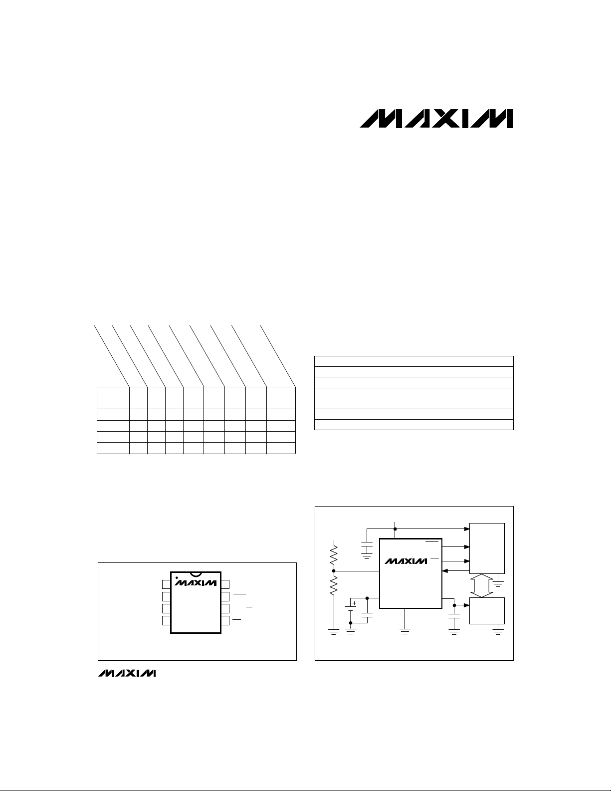
Active-High Reset
Active-Low Reset
Part
MAX690
MAX704
MAX802
MAX804
MAX805
MAX806
Watchdog Input
✓✓ ✓
✓✓✓
✓✓ ✓
✓✓✓
✓✓ ✓
✓✓ ✓
Threshold Accuracy
Backup-Battery
Manual Reset
Switch
Input
Comparator
Power-Fail
Power-Fail
±4%
±4%
±2%
±2%
±4%
±2%
Reset Window
✓
±75mV
✓
±75mV
✓
±2%
✓
±2%
✓
±75mV
✓
±2%
________________________Applications
Battery-Powered Computers and Controllers
Embedded Controllers
Intelligent Instruments
Automotive Systems
Critical µP Power Monitoring
Portable Equipment
__________________Pin Configuration
TOP VIEW
1
V
OUT
MAX690T/S/R
2
MAX704T/S/R
V
CC
MAX802T/S/R
3
GND
MAX804T/S/R
MAX805T/S/R
4
PFI
MAX806T/S/R
( )
ARE FOR MAX804T/S/R, MAX805T/S/R
< > ARE FOR MAX704T/S/R, MAX806T/S/R
DIP/SO
8
VBATT
7
RESET (RESET)
6
WDI
<MR>
5
PFO
____________________________Features
♦–R—E—S—E—T–and RESET Outputs
♦ Manual Reset Input
♦ Precision Supply-Voltage Monitor
♦ 200ms Reset Time Delay
♦ Watchdog Timer (1.6sec timeout)
♦ Battery-Backup Power Switching—
Battery Can Exceed VCCin Normal Operation
♦ 40µA VCCSupply Current
♦ 1µA Battery Supply Current
♦ Voltage Monitor for Power-Fail or
Low-Battery Warning
♦ Guaranteed –R—E—S—E—T– Assertion to VCC= 1V
♦ 8-Pin DIP and SO Packages
______________Ordering Information
PART** TEMP. RANGE
MAX690_CPA
MAX690_CSA 0°C to +70°C
MAX690_C/D 0°C to +70°C Dice*
MAX690_EPA -40°C to +85°C
MAX690_ESA -40°C to +85°C
MAX690_MJA -55°C to +125°C 8 CERDIP
0°C to +70°C
Ordering Information continued on last page.
* Contact factory for dice specifications.
** These parts offer a choice of reset threshold voltage. Select
the letter corresponding to the desired nominal reset threshold
voltage (T = 3.075V, S = 2.925V, R = 2.625V) and insert it into
the blank to complete the part number.
PIN-PACKAGE
8 Plastic DIP
8 SO
8 Plastic DIP
8 SO
_________Typical Operating Circuits
REGULATED +3.3V OR +3.0V
V
UNREGULATED
DC
0.1µF
R1
3.6V
R2
LITHIUM
BATTERY
( ) ARE FOR MAX804T/S/R, MAX805T/S/R
See last page for MAX704T/S/R, MAX806T/S/R.
PFI
VBATT
0.1µF
V
CC
MAX690T/S/R
MAX802T/S/R
MAX804T/S/R
MAX805T/S/R
GND
RESET
(RESET)
PFO
V
WDI
OUT
0.1µF
CC
RESET
NMI
I/O LINE
BUS
V
CC
CMOS RAM
µP
GND
GND
MAX690T/S/R, 704T/S/R, 802T/S/R, 804–806T/S/R
________________________________________________________________
Maxim Integrated Products
Call toll free 1-800-998-8800 for free samples or literature.
1

3.0V/3.3V Microprocessor Supervisory Circuits
ABSOLUTE MAXIMUM RATINGS
Terminal Voltage (with respect to GND)
.........................................................................-0.3V to 6.0V
V
CC
VBATT....................................................................-0.3V to 6.0V
All Other Inputs ...................-0.3V to the higher of V
Continuous Input Current
..................................................................................100mA
V
CC
VBATT...............................................................................18mA
or VBATT
CC
GND..................................................................................18mA
Output Current
–R—E—S—E—T–, –P—F—O–
V
OUT
Stresses beyond those listed under “Absolute Maximum Ratings” may cause permanent damage to the device. These are stress ratings only, and functional
operation of the device at these or any other conditions beyond those indicated in the operational sections of the specifications is not implied. Exposure to
absolute maximum rating conditions for extended periods may affect device reliability.
....................................................................18mA
................................................................................100mA
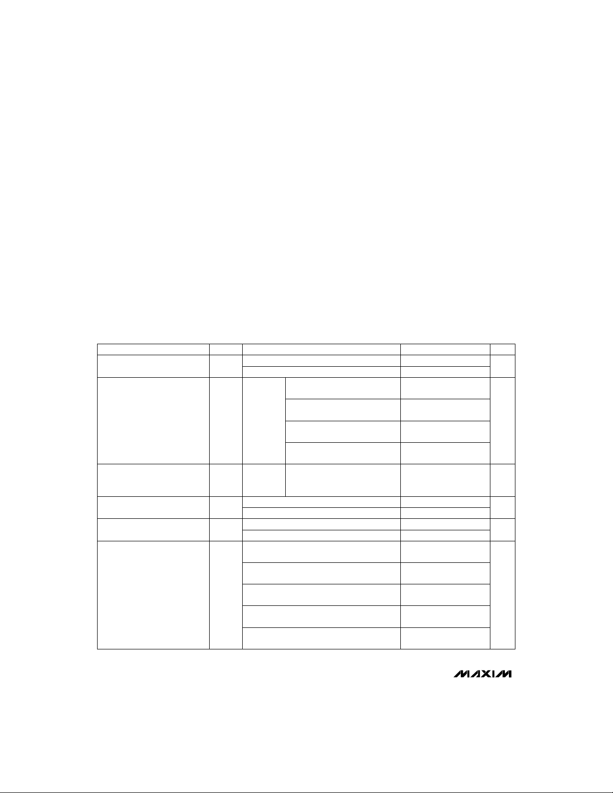
ELECTRICAL CHARACTERISTICS
(VCC= 3.17V to 5.5V for the MAX690T/MAX704T/MAX80_T, VCC= 3.02V to 5.5V for the MAX690S/MAX704S/MAX80_S, VCC= 2.72V to
5.5V for the MAX690R/MAX704R/MAX80_R; VBATT = 3.6V; T
Operating Voltage Range,
, VBATT (Note 1)
V
CC
MAX690_C, MAX704_C, MAX80_ _C
MAX690_E/M, MAX704_E/M, MAX80_ _E/M
–M—R–
VCCSupply Current
(excluding I
OUT
)
I
SUPPLY
(MAX704_/
MAX806_)
–M—R–
VCCSupply Current in BatteryBackup Mode (excluding I
OUT
)
VBATT Supply Current, Any Mode
(excluding I
OUT
) (Note 2)
Battery Leakage Current
(Note 3)
(MAX704_/
MAX806_)
MAX690_C/E, MAX704_C/E, MAX80_ _C/E
MAX690_M, MAX704_M, MAX80_ _M
MAX690_C/E, MAX704_C/E, MAX80_ _C/E
MAX690_M, MAX704_M, MAX80_ _M
MAX690_C/E, MAX704_C/E, MAX80_ _C/E,
I
OUT
MAX690_C/E, MAX704_C/E, MAX80_ _C/E
I
OUT
V
Output Voltage V
OUT
MAX690T/S/R, 704T/S/R, 802T/S/R, 804–806T/S/R
MAX690_M, MAX704_M, MAX80_ _M
I
OUT
MAX690_M, MAX704_M, MAX80_ _M
I
OUT
I
OUT
A
= V
CC
= V
CC
= 5mA (Note 4)
= 50mA
= 5mA (Note 4)
= 50mA
= 250µA, VCC> 2.5V (Note 4)
Continuous Power Dissipation (T
Plastic DIP (derate 9.09mW/°C above +70°C) ..............727mW
= +70°C)
A
SO (derate 5.88mW/°C above +70°C)...........................471mW
CERDIP (derate 8.00mW/°C above +70°C)...................640mW
Operating Temperature Ranges
MAX690_C_ _/MAX704_C_ _/MAX80_ _C_ _........0°C to +70°C
MAX690_E_ _/MAX704_E_ _/MAX80_ _E_ _......-40°C to +85°C
MAX690_M_ _/MAX704_M_ _/MAX80_ _M_ _...-55°C to +125°C
Storage Temperature Range.............................-65°C to +160°C
Lead Temperature (soldering, 10sec).............................+300°C
= T
to T
MIN
; unless otherwise noted. Typical values are at TA= +25°C.)
MAX
CONDITIONS
1.0 5.5
1.1 5.5
MAX690_C/E, MAX704_C/E,
MAX80_ _C/E, VCC< 3.6V
MAX690_C/E, MAX704_C/E,
MAX80_ _C/E, VCC< 5.5V
MAX690_M, MAX704_M,
MAX80_ _M, VCC< 3.6V
MAX690_M, MAX704_M,
MAX80_ _M, V
CC
< 5.5V
40 50
50 65
40 55
50 70
VCC= 2.0V, VBATT = 2.3V
0.4 1
0.4 10
0.01 0.5
0.01 5
V
-V
CC
CC
0.03 0.015
V
-V
CC
CC
0.3 0.15
V
-V
CC
CC
0.035 0.015
V
-V
CC
CC
0.35 0.15
V
-V
CC
CC
0.0015 0.0006
UNITSMIN TYP MAXSYMBOLPARAMETER
V
µA
µA25 50
µA
µA
-
-
-
-
-
2 _______________________________________________________________________________________

3.0V/3.3V Microprocessor Supervisory Circuits
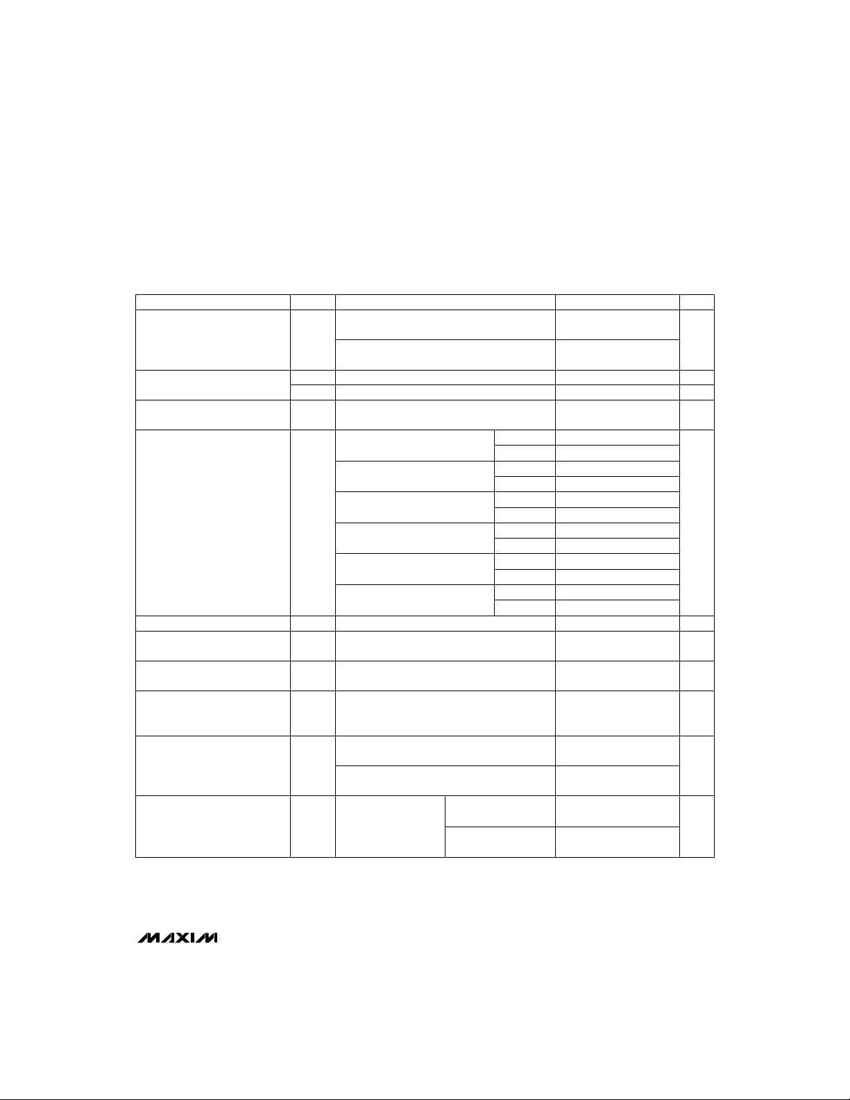
ELECTRICAL CHARACTERISTICS (continued)
(VCC= 3.17V to 5.5V for the MAX690T/MAX704T/MAX80_T, VCC= 3.02V to 5.5V for the MAX690S/MAX704S/MAX80_S, VCC= 2.72V to
5.5V for the MAX690R/MAX704R/MAX80_R; VBATT = 3.6V; T
I
V
in Battery-Backup Mode
OUT
Battery Switch Threshold,
VCCFalling
Battery Switch Threshold,
VCCRising (Note 7)
OUT
I
OUT
VBATT - V
VBATT > VCC(Note 6)
SW
This value is identical to the reset threshold,
VCCrising
MAX690T/704T/805T
MAX802T/804T/806T
MAX690S/704S/805S
Reset Threshold (Note 8)
V
RST
MAX802S/804S/806S
MAX690R/704R/805R
MAX802R/804R/806S
Reset Timeout Period
–P—F—O–, –R—E—S—E—T–
–P—F—O–, –R—E—S—E—T–
Output Voltage
Output Short to
GND Current (Note 4)
–P—F—O–, –R—E—S—E—T–
, RESET
Output Voltage
VCC< 3.6V
WP
V
I
OH
SOURCE
VCC= 3.3V, VOH= 0V
OS
I
SINK
MAX690_/704_/802_/806_, VCC= V
OL
MAX804_/805_, VCC= V
VBATT = 0V, VCC= 1.0V, I
–P—F—O–, –R—E—S—E—T–
Output Voltage
MAX690_C, MAX704_C, MAX80_ _C
V
OL
VBATT = 0V, VCC= 1.2V, I
MAX690_E/M, MAX704_E/M, MAX80_ _E/M
RESET Output Leakage Current
(Note 9)
VBATT = 0V,
VCC= V
V
RESET
= T
to T
A
MIN
MAX
CONDITIONS
= 250µA, VBATT = 2.3V
= 1mA, VBATT = 2.3V
> VCC> 1.75V (Note 5)
CC,VSW
= 50µA
= 1.2mA;
RST
MAX804_C,
min;
RST
= 0V, V
CC
MAX805_C
MAX804_E/M,
MAX805_E/M
; unless otherwise noted. Typical values are at TA= +25˚C.)
UNITSMIN TYP MAXSYMBOLPARAMETER
VBATT VBATT
- 0.1 - 0.034
VBATT
- 0.14
mV65 25
VCCfalling
VCCrising
VCCfalling
VCCrising
VCCfalling
VCCrising
VCCfalling
VCCrising
VCCfalling
VCCrising
VCCfalling
VCCrising
3.00 3.075 3.15
3.00 3.085 3.17
3.00 3.075 3.12
3.00 3.085 3.14
2.85 2.925 3.00
2.85 2.935 3.02
2.88 2.925 3.00
2.88 2.935 3.02
2.55 2.625 2.70
2.55 2.635 2.72
2.59 2.625 2.70
2.59 2.635 2.72
ms140 200 280t
V
V
CC
CC
- 0.3 - 0.05
µV180 500I
min;
RST
max
= 40µA,
SINK
SINK
= 200µA,
0.13 0.3
0.17 0.3
-1 1
µA
-10 10
V
V2.30 2.40 2.50V
V
V
V
V0.06 0.3V
V
MAX690T/S/R, 704T/S/R, 802T/S/R, 804–806T/S/R
_______________________________________________________________________________________ 3

3.0V/3.3V Microprocessor Supervisory Circuits
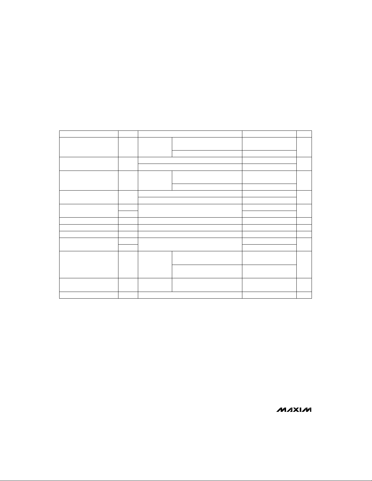
ELECTRICAL CHARACTERISTICS (continued)
(VCC= 3.17V to 5.5V for the MAX690T/MAX704T/MAX80_T, VCC= 3.02V to 5.5V for the MAX690S/MAX704S/MAX80_S, VCC= 2.72V to
5.5V for the MAX690R/MAX704R/MAX80_R; VBATT = 3.6V; T
SYMBOLPARAMETER UNITS
VCC< 3.6V
PFI Input Threshold
PFI Input Current
PFI Hysteresis, PFI Rising
PFI Input Current
–M—R–
Input Threshold
–M—R–
Pulse Width
–M—R–
to Reset Delay
–M—R–
Pull-Up Current
WDI Input Threshold
V
PFT
V
falling
PFI
MAX690_C/E, MAX704_C/E, MAX80_ _C/E
MAX690_M, MAX704_M, MAX80_ _M
V
VCC< 3.6V
PFH
MAX690_C/E, MAX704_C/E, MAX80_ _C/E
MAX690_M, MAX704_M, MAX80_ _M
V
IH
MAX704_/MAX806_ only
V
IL
MAX704_/MAX806_ only
MR
MAX704_/MAX806_ only
MD
MAX704_/MAX806_ only, –M—R–= 0V, VCC= 3V
V
IH
MAX690_/MAX802_/MAX804_/MAX805_ only
V
IL
0V< VCC< 5.5V
Watchdog Timeout Period
WD
VCC< 3.6V
MAX690_/MAX802_/MAX804_/MAX805_ only
Note 1: VCCsupply current, logic input leakage, watchdog functionality (MAX690_/802_/805_/804_), –M—R–functionality
(MAX704_/806_), PFI functionality, state of –R—E—S—E—T–(MAX690_/704_/802_/806_), and RESET (MAX804_/805_) tested at
VBATT = 3.6V, and V
Note 2: Tested at VBATT = 3.6V, V
= 1.9V.
V
Note 3: Leakage current into the battery is tested under the worst-case conditions at V
CC
= 5.5V. The state of –R—E—S—E—T–or RESET and –P—F—O–is tested at VCC= VCCmin.
CC
= 3.5V and 0V. The battery current will rise to 10µA over a narrow transition window around
CC
VBATT= 1.0V.
Note 4: Guaranteed by design.
Note 5: When V
has a small 25mV typical hysteresis to prevent oscillation. For V
MAX690T/S/R, 704T/S/R, 802T/S/R, 804–806T/S/R
voltage on VBATT.
Note 6: When VBATT > V
Note 7: V
V
switchover occurs 200ms prior to reset.
> VCC> VBATT, V
SW
> VSW, V
switches from VBATT to VCCwhen VCCrises above the reset threshold, independent of VBATT. Switchover back to
OUT
occurs at the exact voltage that causes –R—E—S—E—T–to go high (on the MAX804_/805_, RESET goes low); however
CC
CC
remains connected to VCCuntil VCCdrops below VBATT. The VCC-to-VBATT comparator
OUT
remains connected to VCCuntil VCCdrops below the battery switch threshold (VSW).
OUT
Note 8: The reset threshold tolerance is wider for V
prevents internal oscillation.
Note 9: The leakage current into or out of the RESET pin is tested with RESET asserted (RESET output high impedance).
= T
to T
A
MIN
CONDITIONS
MAX802_C/E, MAX804_C/E,
MAX806_C/E
MAX690_/MAX704_/MAX805_
; unless otherwise noted. Typical values are at TA= +25˚C.)
MAX
MIN TYP MAX
1.212 1.237 1.262
1.187 1.237 1.287
-25 2 25
-500 2 500
MAX690_C/E, MAX704_C/E,
MAX80_ _C/E
MAX690_M, MAX704_M, MAX80_ _M
10 20
10 25
-25 2 25
-500 2 500
0.7 x V
CC
0.3 x V
CC
0.7 x V
CC
0.3 x V
CC
MAX690_C/E, MAX802_C/E,
MAX804_C/E, MAX805_C/E
MAX690_M, MAX802_M,
MAX804_M, MAX805_M
MAX690/MAX802/MAX804/
MAX805 only
CC
< 1.75V (typ), V
CC
rising than for VCCfalling to accommodate the 10mV typical hysteresis, which
CC
-1 0.01 1
-10 0.01 10
1.12 1.60 2.24
= 5.5V, VBATT = 1.8V and at VCC= 1.5V,
switches to VBATT regardless of the
OUT
V
nA
mV
nA
V
ns100 20t
ns60 500t
µA20 60 350
V
µAWDI Input Current
sect
ns100 20WDI Pulse Width
4 _______________________________________________________________________________________
 Loading...