

19-4333; Rev 3; 9/93
RESET
Microprocessor Supervisory Circuits
__________________General Description
The MAX690A/MAX692A/MAX802L/MAX802M/MAX805L
reduce the complexity and number of components
required for power-supply monitoring and battery-control
functions in microprocessor (µP) systems. They significantly improve system reliability and accuracy compared
to separate ICs or discrete components.
These parts provide four functions:
1) A reset output during power-up, power-down, and
brownout conditions.
2) Battery-backup switching for CMOS RAM, CMOS
µP, or other low-power logic.
3) A reset pulse if the optional watchdog timer has not
been toggled within 1.6sec.
4) A 1.25V threshold detector for power-fail warning or
low-battery detection, or to monitor a power supply
other than +5V.
The parts differ in their reset-voltage threshold levels
and reset outputs. The MAX690A/MAX802L/MAX805L
generate a reset pulse when the supply voltage drops
below 4.65V, and the MAX692A/MAX802M generate a
reset below 4.40V. The MAX802L/MAX802M guarantee power-fail accuracies to ±2%. The MAX805L is the
same as the MAX690A except that RESET is provided
instead of RESET.
All parts are available in 8-pin DIP and SO packages.
The MAX690A/MAX802L are pin compatible with the
MAX690 and MAX694. The MAX692A/MAX802M are
pin compatible with the MAX692.
_______________________Applications
Battery-Powered Computers and Controllers
Intelligent Instruments
Automotive Systems
Critical µP Power Monitoring
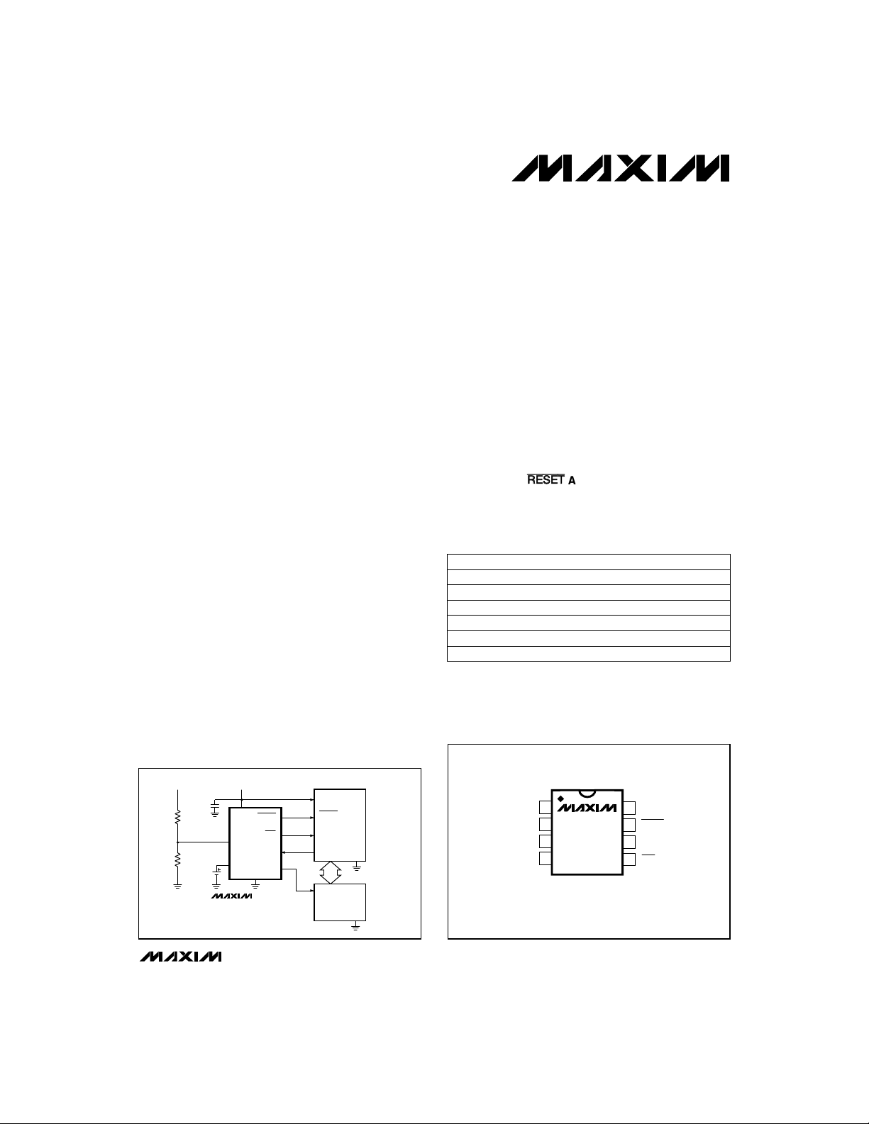
__________Typical Operating Circuit
UNREGULATED DC REGULATED +5V
V
O.1µF
R
1
3.6V
R
2
LITHIUM
BATTERY
PFI
V
MAX690A
MAX802L
V
BATT
CC
RESET
PFO
WDI
V
OUT
GND
CC
RESET
NMI
I/O LINE
BUS
V
CC
CMOS
RAM
µP
GND
GND
___________________________Features
♦ Precision Supply-Voltage Monitor:
4.65V for MAX690A/MAX802L/MAX805L
4.40V for MAX692A/MAX802M
♦ Reset Time Delay – 200ms
♦ Watchdog Timer – 1.6sec Timeout
♦ Battery-Backup Power Switching
♦ 200µA Quiescent Supply Current
♦ 50nA Quiescent Supply Current in Battery-
Backup Mode
♦ Voltage Monitor for Power-Fail or Low-Battery
Warning
♦ Power-Fail Accuracy Guaranteed to ±2%
(MAX802L/M)
♦ Guaranteed
♦ 8-Pin SO and DIP Packages
Assertion to VCC= 1V
______________Ordering Information
PART TEMP. RANGE PIN-PACKAGE
MAX690ACPA
MAX690ACSA 0°C to +70°C 8 SO
MAX690AC/D 0°C to +70°C Dice*
MAX690AEPA -40°C to +85°C 8 Plastic DIP
MAX690AESA -40°C to +85°C 8 SO
MAX690AMJA -55°C to +125°C 8 CERDIP**
Ordering Information continued on last page.
* Dice are specified at T
**Contact factory for availability and processing to MIL-STD-883.
0°C to +70°C
= +25°C
A
8 Plastic DIP
_________________Pin Configurations
TOP VIEW
V
OUT
1
PFI
MAX690A
2
CC
MAX692A
MAX802L
3
MAX802M
4
MAX805L
DIP/SO
V
GND
( ) ARE FOR MAX805L ONLY.
8
BATT
V
RESET (RESET)
7
WDI
6
5
PFO
MAX690A/MAX692A/MAX802L/MAX802M/MAX805L
________________________________________________________________
Maxim Integrated Products
Call toll free 1-800-998-8800 for free samples or literature.
1
Microprocessor Supervisory Circuits
ABSOLUTE MAXIMUM RATINGS
Terminal Voltage (with respect to GND)
............................................... -0.3V to 6.0V
V
CC
.............................................. -0.3V to 6.0V
V
BATT
All Other Inputs (Note 1) ................ -0.3V to (V
Input Current
...................................................... 200mA
V
CC
..................................................... 50mA
V
BATT
GND ...................................................... 20mA
Output Current
................... Short-Circuit Protected for up to 10sec
V
OUT
All Other Outputs ........................................ 20mA
CC
+ 0.3V)
Note 1: The input voltage limits on PFI and WDI may be exceeded if the current into these pins is limited to less than 10mA.
Stresses beyond those listed under "Absolute Maximum Ratings" may cause permanent damage to the device. These are stress ratings only, and functional
operation of the device at these or any other conditions beyond those indicated in the operational sections of the specifications is not implied. Exposure to
absolute maximum rating conditions for extended periods may affect device reliability.
ELECTRICAL CHARACTERISTICS
(VCC= 4.75V to 5.5V for MAX690A/MAX802L/MAX805L, VCC= 4.5V to 5.5V for MAX692A/MAX802M, V
= T
to T
T
A
MIN
Operating Voltage Range,
, V
V
CC
BATT
Supply Current (Excluding I
I
SUPPLY
(Excluding I
V
Standby Current (Note 3)
BATT
V
Output
OUT
V
in Battery-Backup Mode I
OUT
Battery Switch Threshold, V
to V
BATT
Battery Switchover Hysteresis 40 mV
Reset Threshold
Reset Threshold Hysteresis 40 mV
Reset Pulse Width
MAX690A/MAX692A/MAX802L/MAX802M/MAX805L
RESET Output Voltage
, unless otherwise noted.)
MAX
PARAMETER SYMBOL CONDITIONS MIN TYP MAX UNITS
MAX69_AC, MAX802_C 1.0 5.5
(Note 2)
OUT
in Battery-Backup Mode
)
OUT
) I
SUPPLY
MAX69_AE/M, MAX80_ _E 1.2 5.5
MAX69_AC, MAX802_C 200 350
MAX69_AE/M, MAX802_E, MAX805LE/M 200 500
VCC= 0V,
V
BATT
5.5V > VCC>
V
BATT
I
= 5mA VCC- 0.05 VCC- 0.025
OUT
I
= 50mA
OUT
= 250µA, VCC< V
OUT
CC
VCC< V
MAX690A, MAX802L, MAX805L
MAX692A, MAX802M 4.25 4.40 4.50
V
RT
MAX802L, TA= +25°C, VCCfalling
MAX802M, TA= +25°C, VCCfalling
t
RS
I
SOURCE
I
= 3.2mA
SINK
MAX69_AC, MAX802_C, VCC= 1.0V
= 50µA
I
SINK
MAX69_AE/M, MAX802_E,
= 1.2V, I
V
CC
Rate of Rise, V
Continuous Power Dissipation
, V
CC
................................ 100V/µs
BATT
Plastic DIP (derate 9.09mW/°C above +70°C) ........ 727mW
SO (derate 5.88mW/°C above +70°C) ................ 471mW
CERDIP (derate 8.00mW/°C above +70°C) ........... 640mW
Operating Temperature Ranges:
MAX69_AC_ _, MAX80_ _ C_ _ .................. 0°C to +70°C
MAX69_AE_ _, MAX80_ _ E_ _ ................ -40°C to +85°C
MAX69_AMJA, MAX805LMJA................ -55°C to +125°C
Storage Temperature Range .................. -65°C to +160°C
Lead Temperature (soldering, 10sec) .................. +300°C
1.1 5.5
= 2.8V
+0.2V
TA= +25°C
TA= T
MIN
TA= +25°C
TA= T
MIN
to T
to T
MAX
MAX
0.05 1.0
-0.1 0.02
-1.0 0.02
VCC- 0.5 VCC- 0.25
- 0.2V V
BATT
RT
Power-up
Power-down
BATT
- 0.1 V
BATT
20
-20
4.50 4.65 4.75
4.55 4.70
4.30 4.45
140 200 280 ms
= 800µA VCC- 1.5
= 100µA
SINK
- 0.02
5.0
0.4
0.3
0.3
BATT
= 2.8V,
VMAX805LC
µA
µA
µA
V
V
mV
V
V
2 _______________________________________________________________________________________
Microprocessor Supervisory Circuits
ELECTRICAL CHARACTERISTICS (continued)
(VCC= 4.75V to 5.5V for MAX690A/MAX802L/MAX805L, VCC= 4.5V to 5.5V for MAX692A/MAX802M, V
= T
to T
T
A
MIN
, unless otherwise noted.)
MAX
PARAMETER SYMBOL CONDITIONS MIN TYP MAX UNITS
RESET Output Voltage
Watchdog Timeout
WDI Pulse Width
WDI Input Threshold (Note 4)
WDI Input Current
PFI Input Threshold
MAX805LC, I
MAX805LE/M, I
MAX805L, I
MAX805L, I
t
WD
t
VIL= 0.4V, VIH= (0.8) (VCC)
WP
VCC= 5V
WDI = V
CC
WDI = 0V -150 -50
MAX69_A, MAX805L, VCC= 5V
MAX802_C/E, VCC= 5V
= 4µA, VCC= 1.1V
SOURCE
SOURCE
SINK
= 4µA, VCC= 1.2V
SOURCE
= 800µA VCC- 1.5
= 3.2mA
Logic low
Logic high
0.8
0.9
1.00 1.60 2.25 sec
50 ns
3.5
50 150
1.20 1.25 1.30
1.225 1.250 1.275
PFI Input Current -25 0.01 25 nA
I
= 800µA VCC- 1.5
PFO Output Voltage
Note 2: Either VCCor V
Note 3: "-" = battery-charging current, "+" = battery-discharging current.
can go to 0V, if the other is greater than 2.0V.
BATT
Note 4: WDI is guaranteed to be in an intermediate, non-logic level state if WDI is floating and V
WDI is internally biased to 35% of V
SOURCE
I
= 3.2mA
SINK
with an input impedance of 50kΩ.
CC
is in the operating voltage range.
CC
BATT
0.4
0.8
0.4
MAX690A/MAX692A/MAX802L/MAX802M/MAX805L
= 2.8V,
V
V
µA
V
V
_______________________________________________________________________________________ 3
Microprocessor Supervisory Circuits
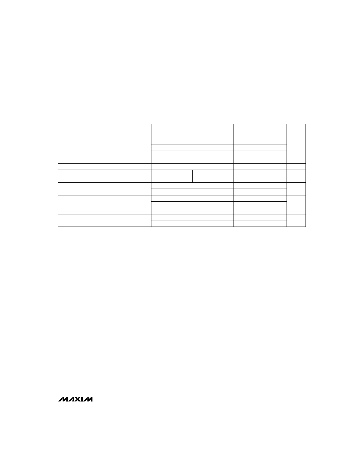
__________________________________________Typical Operating Characteristics
5.00
4.95
4.90
(V)
OUT
V
4.85
4.80
4.75
RESET
+5V
V
+5V
0
CC
V
CC
OUTPUT VOLTAGE
vs. LOAD CURRENT
VCC = +5V
= +2.8V
V
BATT
= +25°C
T
A
SLOPE = 5Ω
20
10 30 50
I
OUT
MAX690A
RESET RESPONSE TIME
V
CC
10k
RESET
30pF
GND
2µs/div
40
(mA)
TA = +25°C
RESET
+4V
1V/div
0V
2.80
2.78
2.76
(V)
OUT
V
2.74
2.72
2.70
+1.30V
SLOPE = 80Ω
0
0.2 0.6 1.0
POWER-FAIL COMPARATOR
+5V
PFO
PFI
+1.25V
PFI
OUTPUT VOLTAGE
vs. LOAD CURRENT
0.4
I
(mA)
OUT
RESPONSE TIME
+5V
1k
PFO
30pF
VCC = +5V
= +25°C
T
A
400ns/div
VCC = 0V
V
BATT
= +25°C
T
A
= +2.8V
0.8
+0V
+1.2V
V
CC
0V
RESET
0V
PFO
PFI
+1.20V
RESET OUTPUT VOLTAGE
vs. SUPPLY VOLTAGE
V
CC
POWER-FAIL COMPARATOR
PFI
+1.25V
0V
MAX690A
V
= OV
BATT
TA = +25°C
V
CC
RESET
GND
500ms/div
RESPONSE TIME
+5V
PFO
30pF 1k
400ns/div
2k
RESET
330pF
VCC = +5V
T
= +25°C
A
+5V
1V/div
+5V
1V/div
+3V
+1.3V
MAX805L
RESET OUTPUT VOLTAGE
vs. SUPPLY VOLTAGE
V
CC
V
0V
MAX690A/MAX692A/MAX802L/MAX802M/MAX805L
RESET
0V
V
BATT
RESET
GND
CC
500ms/div
10k
330
pF
+5V
1V/div
+5V
1V/div
+5V
V
CC
RESET
0V
0V
RESET RESPONSE TIME
V
CC
GND
MAX805L
10k
+4V
330pF
+4V
2µs/div
4 _______________________________________________________________________________________

Microprocessor Supervisory Circuits
______________________________________________________________Pin Description
PIN
MAX690A/MAX692A
MAX802L/MAX802M
MAX805L
1 1
2 2
3 3 GND Ground
4 4 PFI
5 5
6 6 WDI
7
NAME FUNCTION
Supply Output for CMOS RAM. When VCCis above the reset threshold,
connects to VCCthrough a P-channel MOSFET switch. When V
V
V
OUT
V
CC
OUT
is below the reset threshold, the higher of VCCor V
connected to V
OUT
.
+5V Supply Input
Power-Fail Comparator Input. When PFI is less than 1.25V, PFO goes
when not used.
CC
PFO
low. Connect PFI to GND or V
Power-Fail Output. When PFI is less than 1.25V, PFO goes low;
otherwise PFO stays high.
Watchdog Input. If WDI remains high or low for 1.6sec, the internal
watchdog timer runs out and reset is triggered. If WDI is left floating or
connected to a high-impedance three-state buffer, the watchdog
feature is disabled. The internal watchdog timer clears whenever reset
is asserted, WDI is three-stated, or WDI sees a rising or falling edge.
Reset Output. Whenever RESET is triggered, it pulses low for 200ms. It
RESET
stays low when V
MAX690A/MAX802L and 4.4V in the MAX692A/MAX802M) and remains
low for 200ms after V
timeout also triggers RESET.
is below the reset threshold (4.65V in the
CC
rises above the reset threshold. A watchdog
CC
BATT
will be
CC
MAX690A/MAX692A/MAX802L/MAX802M/MAX805L
– 7 RESET
8 8
V
BATT
_______________________________________________________________________________________ 5
Active-High Reset Output is the inverse of RESET. When RESET is
or V
asserted, the RESET output voltage = V
higher.
CC
, whichever is
BATT
Backup-Battery Input. When VCCfalls below the reset threshold, V
will be switched to V
rises to 20mV above V
hysteresis prevents repeated switching if V
OUT
BATT
if V
is 20mV greater than VCC. When V
BATT
, V
will be reconnected to VCC. The 40mV
OUT
falls slowly.
CC
BATT
CC

Microprocessor Supervisory Circuits
V
BATT
V
CC
WDI
PFI
( ) ARE FOR MAX805L ONLY.
Figure 1. Block Diagram
_______________Detailed Description
A microprocessor’s (µP’s) reset input starts the µP in a
known state. When the µP is in an unknown state, it should
be held in reset. The MAX690A/MAX692A/MAX802L/
MAX802M assert reset during power-up and prevent code
execution errors during power-down or brownout conditions.
On power-up, once VCCreaches 1V, RESET is guaran-
BATTERY-SWITCHOVER
CIRCUITRY
3.5V
1.25V
0.8V
1.25V
WATCHDOG
TIMER
GND
RESET
GENERATOR
MAX690A
MAX692A
MAX802L
MAX802M
MAX805L
Reset Output
V
OUT
RESET
(RESET)
PFO
Figure 2. Timing Diagram
ed, the watchdog timer remains clear. When RESET
comes high, the watchdog resumes timing and must be
serviced within 1.6sec. If WDI is tied high or low, a
RESET pulse is triggered every 1.8sec (t
The MAX805L active-high RESET output is the inverse
of the MAX690A/MAX692A/MAX802L/MAX802M RESET
output, and is guaranteed to be valid with VCCdown to
1.1V. Some µPs, such as Intel’s 80C51, require an
active-high reset pulse.
teed to be a logic low. As VCCrises, RESET remains
low. When VCCexceeds the reset threshold, an internal
timer keeps RESET low for a time equal to the reset
pulse width; after this interval, RESET goes high (Figure
2). If a brownout condition occurs (if VCCdips below
the reset threshold), RESET is triggered. Each time
RESET is triggered, it stays low for the reset pulse width
interval. Any time VCCgoes below the reset threshold,
the internal timer restarts the pulse. If a brownout condition interrupts a previously initiated reset pulse, the
The watchdog circuit monitors the µP’s activity. If the
µP does not toggle the watchdog input (WDI) within
1.6sec, a reset pulse is triggered. The internal 1.6sec
timer is cleared by either a reset pulse or by open circuiting the WDI input. As long as reset is asserted or
the WDI input is open circuited, the timer remains
cleared and does not count. As soon as reset is
released or WDI is driven high or low, the timer starts
counting. It can detect pulses as short as 50ns.
reset pulse continues for another 200ms. On powerdown, once VCCgoes below the threshold, RESET is
MAX690A/MAX692A/MAX802L/MAX802M/MAX805L
guaranteed to be logic low until VCCdroops below 1V.
RESET is also triggered by a watchdog timeout. If a
high or low is continuously applied to the WDI pin for
1.6sec, RESET pulses low. As long as RESET is assert-
The PFI input is compared to an internal 1.25V refer-
ence. If PFI is less than 1.25V, PFO goes low. The
power-fail comparator is intended for use as an under-
voltage detector to signal a failing power supply; it
+5V
V
CC
0V
V
OUT
3.0V
0V
+5V
RESET
0V
+5V
(RESET)
3.0V
0V
+5V
PFO
0V
( ) ARE FOR MAX805L ONLY.
t
RS
= PFI = 3.0V
V
BATT
= 0mA
I
OUT
plus tRS).
WD
Watchdog Input
Power-Fail Comparator
6 _______________________________________________________________________________________

Microprocessor Supervisory Circuits
V
BATT
SW2
SW1
D1
D2
SUBSTRATE
MAX690A
MAX692A
V
CC
V
CC
V
CC
VCC < Reset Threshold and
V
CC
RESET THRESHOLD = 4.65V IN MAX690A/MAX802L/MAX805L.
RESET THRESHOLD = 4.4V IN MAX692A/MAX802M
MAX805L
MAX802L
MAX802M
> Reset Threshold Open
< Reset Threshold and
> V
BATT
< V
BATT
D3
V
OUT
SW1/SW2
Open
Closed
SW3
SW3/SW4CONDITION
Closed
Closed
Open
SW4
V
CC
Figure 3. Backup-Battery Switchover Block Diagram
need not be dedicated to this function though, as it is
completely separate from the rest of the circuitry. The
external voltage divider drives PFI to sense the unregulated DC input to the +5V regulator (see
Operating Circuit
). The voltage-divider ratio can be
Typical
chosen such that the voltage at PFI falls below 1.25V
just before the +5V regulator drops out. PFO then triggers an interrupt which signals the µP to prepare for
power-down.
To conserve backup-battery power, the power-fail
detector comparator is turned off and PFO is forced
low when V
connects to V
BATT
OUT
.
Backup-Battery Switchover
In the event of a brownout or power failure, it may be
necessary to preserve the contents of RAM. With a
backup battery installed at V
cally switch RAM to backup power when VCCfails.
As long as VCCexceeds the reset threshold, V
to VCCthrough a 5Ω PMOS power switch. Once VCCfalls
below the reset threshold, VCCor V
er) switches to V
MAX690A/MAX692A/MAX802L/MAX802M/MAX805L don’t
always connect V
VCC. V
when VCCis below the reset threshold and V
connects to V
BATT
. Unlike the MAX690/MAX692, the
OUT
to V
BATT
OUT
, the devices automati-
BATT
connects
OUT
(whichever is high-
BATT
when V
OUT
(through an 80Ω switch) only
is greater than
BATT
BATT
is greater
+5V
MAX690A
MAX802L
MAX805L
GND
V
RESET
(RESET)
OUT
TO STATIC RAM
TO µP
+
0.1F
( ) ARE FOR MAX805L ONLY.
V
CC
V
BATT
Figure 4. Using a SuperCap as a Backup Power Source with a
MAX690A/MAX802L/MAX805L and a +5V ±5% Supply
than V
.
CC
When VCCexceeds the reset threshold, it is connected to
the MAX690A/MAX692A/MAX802L/MAX802M/MAX805L
substrate, regardless of the voltage applied to V
(Figure 3). During this time, the diode (D1) between V
and the substrate will conduct current from V
Table 1. Input and Output Status in Battery-Backup Mode
SIGNAL STATUS
V
CC
V
OUT
V
BATT
PFI Power-fail comparator is disabled.
PFO
RESET
RESET Logic high (MAX805L only)
WDI Watchdog timer is disabled
Disconnected from V
Connected to V
PMOS switch
Connected to V
battery is less than 1µA, as long as
< V
V
CC
BATT
OUT
through an internal 80Ω
BATT
. Current drawn from the
OUT
- 1V.
Logic low
Logic low
BATT
BATT
BATT
to VCCif
MAX690A/MAX692A/MAX802L/MAX802M/MAX805L
_______________________________________________________________________________________ 7

Microprocessor Supervisory Circuits
+5V
MAX692A
MAX802M
GND
V
OUT
RESET
TO STATIC RAM
TO µP
100k
0.1F
V
CC
V
BATT
+
Figure 5. Using a SuperCap™ as a Backup Power Source with
the MAX692A/MAX802M and a +5V ±10% Supply
V
is 0.6V or greater than VCC.
BATT
When V
ed and the internal circuitry is powered from the battery
(Table 1). When VCCis just below V
drawn from V
more than 1V below V
parator shuts off and the supply current falls to less
connects to V
BATT
BATT
, backup mode is activat-
OUT
, the current
is typically 30µA. When VCCdrops to
, the internal switchover com-
BATT
BATT
than 1µA.
__________Applications Information
V
IN
R
1
R
C1*
R
R2R
R2|| R
R1R2|| R
+
5 1.25
R
3
TO µP
2
+
3
=
3
2
3
1.25
R
2
+5V
PFO
0V
R
2
0V
V
TRIP
VIH1.25/
=
VL1.25
−+−
R
1
1.25/
=
Figure 6. Adding Hysteresis to the Power-Fail Comparator
PFI
PFO
+5V
V
CC
MAX690
MAX692A
MAX802L
MAX802M
MAX805L
GND
*OPTIONAL
V
V
L
H
V
TRIP
V
IN
Using a SuperCap™ as a Backup
Power Source
SuperCaps are capacitors with extremely high capacitance values, on the order of 0.1F. Figure 4 shows a
SuperCap used as a backup power source. Do not allow
the SuperCap’s voltage to exceed the maximum reset
threshold by more than 0.6V. In Figure 4’s circuit, the
SuperCap rapidly charges to within a diode drop of VCC.
However, after a long time, the diode leakage current will
pull the SuperCap voltage up to VCC. When using a
SuperCap with the MAX690A/MAX802L/MAX805L, V
may not exceed 4.75V + 0.6V = 5.35V.
Lithium batteries work very well as backup batteries due to
very low self-discharge rates and high energy density.
Single lithium batteries with open-circuit voltages of 3.0V to
3.6V are ideal. Any battery with an open-circuit voltage
less than the minimum reset threshold plus 0.3V can be
CC
Table 2. Allowable Backup-Battery Voltages
Use the SuperCap circuit of Figure 5 with a MAX692A
or MAX802M and a ±10% supply. This circuit
ensures that the SuperCap only charges to VCC-
0.5V. At the maximum VCCof 5.5V, the SuperCap
MAX690A/MAX692A/MAX802L/MAX802M/MAX805L
charges up to 5.0V, only 0.5V above the maximum
reset threshold—well within the requisite 0.6V.
™SuperCap is a trademark of Baknor Industries.
MAX802L/MAX805L
Allowable Backup Power-Source
(see
Using a SuperCap as a Backup Power Source
section for use with a SuperCap)
PART NO.
MAX690A/
MAX692A/
MAX802M
MAXIMUM BACKUP-BATTERY
VOLTAGE (V)
4.80
4.55
Batteries
8 _______________________________________________________________________________________

Microprocessor Supervisory Circuits
connected directly to the V
MAX690A/MAX692A/MAX802L/MAX802M/MAX805L with
no additional circuitry (see the
Typical Operating Circuit
BATT
input of the
However, batteries with open-circuit voltages that are
greater cannot be used for backup, as current is sourced
into the substrate through the diode (D1 in Figure 3) when
VCCis close to the reset threshold.
Operation
Without a Backup Power Source
If a backup power source is not used, ground V
and connect V
switch over to any backup power source, V
to VCC. Since there is no need to
OUT
not need to be switched. A direct connection to V
eliminates any voltage drops across the switch which
may push V
below VCC.
OUT
OUT
BATT
does
CC
Replacing the Backup Battery
The backup battery can be removed while VCCremains
valid, without danger of triggering RESET/RESET. As
long as VCCstays above the reset threshold, batterybackup mode cannot be entered. In other switchover
+5V
+5V
PFO
0V
R
1
R
2
V-
V
CC
MAX690A
PFI
MAX692A
MAX802L
MAX802M
MAX805L
V
TRIP
V-
PFO
GND
0V
ICs where battery-backup mode is entered whenever
V
gets close to VCC, an unconnected V
BATT
).
accumulates leakage charge and triggers
RESET/RESET in error.
Adding Hysteresis to the
Power-Fail Comparator
Hysteresis adds a noise margin to the power-fail comparator and prevents repeated triggering of PFO when
VINis close to its trip point. Figure 6 shows how to add
hysteresis to the power-fail comparator. Select the
ratio of R1and R2such that PFI sees 1.25V when V
falls to its trip point (V
will typically be an order of magnitude greater than R
). R3adds the hysteresis. It
TRIP
or R2(about 10 times either R1or R2). The current
through R1and R2should be at least 1µA to ensure
that the 25nA (max) PFI input current does not shift the
trip point. R3should be larger than 10kΩ so it does not
load down the PFO pin. Capacitor C1 adds additional
noise rejection.
Monitoring a Negative Voltage
The power-fail comparator can be used to monitor a
negative supply rail using the circuit of Figure 7. When
the negative rail is good (a negative voltage of large
magnitude), PFO is low. When the negative rail is
degraded (a negative voltage of lesser magnitude),
PFO goes high. This circuit’s accuracy is affected by
the PFI threshold tolerance, the VCCline, and the resistors.
Interfacing to µPs with
Bidirectional Reset Pins
µPs with bidirectional reset pins, such as the Motorola
68HC11 series, can contend with the
MAX690A/MAX692A/MAX802L/MAX802M RESET out-
put. If, for example, the RESET output is driven high
and the µP wants to pull it low, indeterminate logic levels may result. To correct this, connect a 4.7kΩ resistor between the RESET output and the µP reset I/O, as
in Figure 8. Buffer the RESET output to other system
components
BATT
MAX690A/MAX692A/MAX802L/MAX802M/MAX805L
pin
IN
1
5 1.25
1.25 - V
−
NOTE: V
R
1
Figure 7. Monitoring a Negative Voltage
=
IS NEGATIVE
TRIP
TRIP
R
2
_______________________________________________________________________________________ 9

Microprocessor Supervisory Circuits
BUFFERED RESET TO OTHER SYSTEM COMPONENTS
V
CC
MAX690A
MAX692A
RESET
MAX802L
MAX802M
GND
Figure 8. Interfacing to µPs with Bidirectional Reset I/O
4.7k
RESET
V
GND
CC
MAX690A/MAX692A/MAX802L/MAX802M/MAX805L
10 ______________________________________________________________________________________

Microprocessor Supervisory Circuits
CE
________________________
Nominal Reset Watchdog Power-
Reset Pulse Timeout BackupPart Threshold Width Period Battery Write Com- Reset dog Line High On
Number (V) (ms) (sec) Switch Protect parator Input Output Output Reset Output
MAX690A/692A 4.65/4.40 140 1.6 ✔✔
MAX691A/693A 4.65/4.40 140/adj. 1.6/adj. ✔✔/10ns ✔✔✔✔✔
MAX696 Adj. 35/adj. 1.6/adj. ✔ ✔ ✔✔ ✔✔
MAX697 Adj. 35/adj. 1.6/adj. ✔✔ ✔✔ ✔
MAX700 4.65/adj. 200 - ✔✔
MAX703/704 4.65/4.40 140 - ✔✔✔
MAX705/706 4.65/4.40 140 1.6 ✔✔✔
MAX706P 2.63 140 1.6 ✔✔✔ ✔
MAX706R/S/T 2.63/2.93/ 140 1.6 ✔✔✔
3.08
MAX707/708 4.65/4.40 140 - ✔✔ ✔
MAX708R/S/T 2.63/2.93/ 140 - ✔✔ ✔
3.08
MAX709L/M/ 4.65/4.40/ 140 R/S/T 2.63/2.93/3.08
MAX791 4.65 140 1 ✔✔/10ns ✔ ✔✔✔ ✔✔
MAX792L/M/ 4.65/4.40/ 140 1 ✔/10ns ✔ ✔✔✔ ✔
R/S/T 2.63/2.93/3.08
MAX800L/M 4.60/4.40 140 1.6/adj. ✔✔/10ns ✔/±2% ✔✔ ✔✔
MAX802L/M 4.60/4.40 140 1.6 ✔✔/±2%
MAX805L 4.65 140 1.6 ✔✔ ✔
MAX813L 4.65 140 1.6 ✔✔✔ ✔
MAX820L/M/ 4.65/4.40/ 140 1 ✔/10ns ✔/±2% ✔✔✔ ✔
R/S/T 2.63/2.93/3.08
MAX1232 4.37/4.62 250 0.15/0.60/1.2 ✔✔
MAX1259 - - - ✔✔
Minimum Nominal
- Fail Manual- Watch- Low- Active- Battery-
µ
P Supervisory Circuits
MAX690A/MAX692A/MAX802L/MAX802M/MAX805L
______________________________________________________________________________________ 11

Microprocessor Supervisory Circuits
__Ordering Information (continued)
PART TEMP. RANGE PIN-PACKAGE
MAX692ACPA
MAX692ACSA 0°C to +70°C 8 SO
MAX692AC/D 0°C to +70°C Dice*
MAX692AEPA -40°C to +85°C 8 Plastic DIP
MAX692AESA -40°C to +85°C 8 SO
MAX692AMJA -55°C to +125°C 8 CERDIP**
MAX802LCPA
MAX802LCSA 0°C to +70°C 8 SO
MAX802LEPA -40°C to +85°C 8 Plastic DIP
MAX802LESA -40°C to +85°C 8 SO
MAX802MCPA
MAX802MCSA 0°C to +70°C 8 SO
MAX802MEPA -40°C to +85°C 8 Plastic DIP
MAX802MESA -40°C to +85°C 8 SO
MAX805LCPA
MAX805LCSA 0°C to +70°C 8 SO
MAX805LC/D 0°C to +70°C Dice*
MAX805LEPA -40°C to +85°C 8 Plastic DIP
MAX805LESA -40°C to +85°C 8 SO
MAX805LMJA -55°C to +125°C 8 CERDIP**
* Dice are specified at TA= +25°C.
**Contact factory for availability and processing to MIL-STD-883.
0°C to +70°C 8 Plastic DIP
0°C to +70°C 8 Plastic DIP
0°C to +70°C 8 Plastic DIP
0°C to +70°C 8 Plastic DIP
____________________Chip Topography
V
V
CC
GND
( ) ARE FOR MAX805L ONLY.
TRANSISTOR COUNT: 573;
SUBSTRATE MUST BE LEFT UNCONNECTED.
V
OUT
PFI
0.078"
(1.98mm)
BATT
PFO
RESET (RESET)
WDI
(1.55mm)
0.061"
MAX690A/MAX692A/MAX802L/MAX802M/MAX805L
Maxim cannot assume responsibility for use of any circuitry other than circuitry entirely embodied in a Maxim product. No circuit patent licenses are
implied. Maxim reserves the right to change the circuitry and specifications without notice at any time.
12
__________________Maxim Integrated Products, 120 San Gabriel Drive, Sunnyvale, CA 94086 (408) 737-7600
© 1993 Maxim Integrated Products Printed USA is a registered trademark of Maxim Integrated Products.
 Loading...