19-1086; Rev 0; 6/96
8-Pin µP Supervisory Circuits
with ±1.5% Reset Accuracy
_______________General Description
The MAX801/MAX808 microprocessor (µP) supervisory
circuits monitor and control the activities of +5V µPs by
providing backup-battery switchover, low-line indication, and µP reset. Additional features include a watchdog for the MAX801 and CMOS RAM write protection
for the MAX808.
The MAX801/MAX808 offer a choice of reset-threshold
voltage (denoted by suffix letter): 4.675V (L), 4.575V
(N), and 4.425V (M). These devices are available in
8-pin DIP and SO packages.
________________________Applications
Computers
Controllers
Intelligent Instruments
Critical µP Power Monitoring
Portable/Battery-Powered Equipment
Embedded Systems
Pin Configurations appear at end of data sheet.
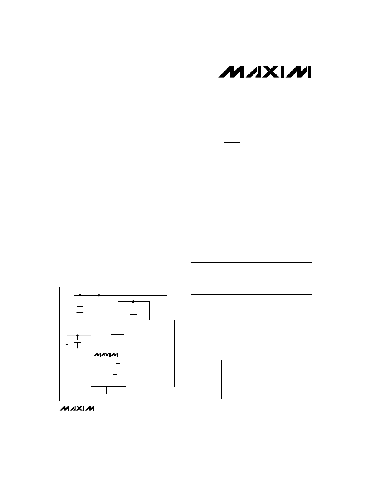
__________Typical Operating Circuit
+5V
0.1µF
0.1µF
BATT
V
CC
MAX808
OUT
LOWLINE
RESET
CE IN
CE OUT
GND
0.1µF
POWER FOR
CMOS RAM
NMI
RESET
µP SYSTEM
FROM I/O SYSTEM OR
ADDRESS DECODER
TO CMOS RAM
µP
POWER
____________________________Features
♦ Precision Voltage Monitoring, ±1.5% Reset
Accuracy
♦ 200ms Power-OK/Reset Time Delay
♦ RESET Output (MAX808)
RESET and RESET Outputs (MAX801)
♦ Watchdog Timer (MAX801)
♦ On-Board Gating of Chip-Enable Signals (MAX808):
Memory Write-Cycle Completion
3ns CE Gate Propagation Delay
♦ 1µA Standby Current
♦ Power Switching:
250mA in VCCMode
20mA in Battery-Backup Mode
♦ MaxCap™/SuperCap™ Compatible
♦ RESET Guaranteed Valid to VCC= 1V
♦ Low-Line Threshold 52mV Above Reset
Threshold
MaxCap is a trademark of The Carborundum Corp.
SuperCap is a trademark of Baknor Industries.
______________Ordering Information
PART*
MAX801_CPA
MAX801_CSA
MAX801_EPA -40°C to +85°C
MAX801_ESA
MAX801_MJA
MAX808_CPA
MAX808_CSA 0°C to +70°C 8 SO
MAX808_EPA
MAX808_ESA
MAX808_MJA -55°C to +125°C
* These parts offer a choice of reset threshold voltage. From the
table below, select the suffix corresponding to the desired
threshold and insert it into the blank to complete the part number.
**Contact factory for availability and processing to MIL-STD-883.
SUFFIX
L 4.60 4.675
N 4.50
M 4.35
TEMP. RANGE PIN-PACKAGE
0°C to +70°C
0°C to +70°C
-40°C to +85°C 8 SO
-55°C to +125°C
0°C to +70°C
-40°C to +85°C 8 Plastic DIP
-40°C to +85°C
RESET THRESHOLD (V)
MIN MAX
8 Plastic DIP
8 SO
8 Plastic DIP
8 CERDIP**
8 Plastic DIP
8 SO
8 CERDIP**
TYP
4.75
4.575 4.65
4.425 4.50
MAX801L/M/N, MAX808L/M/N
________________________________________________________________
Maxim Integrated Products
1
For free samples & the latest literature: http://www.maxim-ic.com, or phone 1-800-998-8800

8-Pin µP Supervisory Circuits
with ±1.5% Reset Accuracy
ABSOLUTE MAXIMUM RATINGS
Input Voltage (with respect to GND)
.......................................................................-0.3V to +6V
V
CC
....................................................................-0.3V to +6V
V
BATT
All Other Pins........................................-0.3V to (V
Input Current
Peak ..........................................................................1.0A
V
CC
Continuous ............................................................500mA
V
CC
Peak.....................................................................250mA
I
BATT
Continuous ............................................................50mA
I
BATT
GND................................................................................50mA
OUT
+ 0.3V)
All Other Inputs...............................................................50mA
Output Current
OUT Peak..........................................................................1.0A
Stresses beyond those listed under “Absolute Maximum Ratings” may cause permanent damage to the device. These are stress ratings only, and functional
operation of the device at these or any other conditions beyond those indicated in the operational sections of the specifications is not implied. Exposure to
absolute maximum rating conditions for extended periods may affect device reliability.
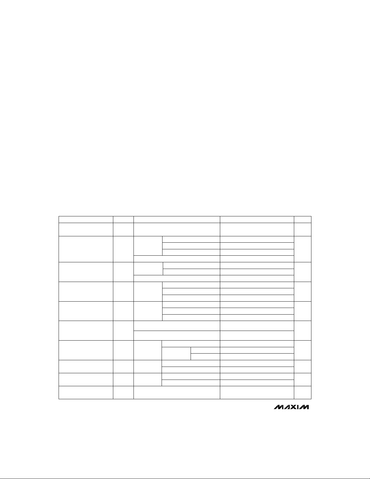
ELECTRICAL CHARACTERISTICS
(VCC= 4.6V to 5.5V for the MAX80_L, VCC= 4.5V to 5.5V for the MAX80_N, VCC= 4.35V to 5.5V for the MAX80_M; V
T
= T
to T
A
MIN
Operating Voltage Range
, BATT (Note 1)
V
CC
V
in Normal Operating
OUT
Mode
MAX801L/M/N, MAX808L/M/N
VCCto OUT
On-Resistance
V
in Battery-Backup
OUT
Mode
BATT to OUT
On-Resistance
Supply Current in Normal
Operating Mode
(excludes I
Supply Current in BatteryBackup Mode (excludes
I
) (Note 2)
OUT
BATT Standby Current
(Note 3)
Battery-Switchover
Threshold
Battery-Switchover
Hysteresis
. Typical values are at VCC= 5V and TA= +25°C, unless otherwise noted.)
MAX
CONDITIONS
I
= 25mA VCC- 0.02
OUT
I
VCC= 4.5V VCC- 0.38 VCC- 0.25
VCC= 3V, V
VCC= 4.5V,
I
= 250mA
OUT
VCC= 3V, I
VCC= 0V V
VCC= 0V Ω
= 250mA, MAX80_C/E
OUT
I
= 250mA, MAX80_M VCC- 0.45
OUT
= 2.8V, I
BATT
MAX80_C/E
MAX80_M
= 100mA
OUT
V
BATT
V
BATT
V
BATT
V
BATT
V
BATT
V
BATT
MAX801
OUT
)
MAX808
VCC= 0V,
V
= 2.8V
BATT
V
+ 0.2V
BATT
≤ V
CC
V
= 2.8V
BATT
TA= +25°C
TA= T
MIN
to T
MAX
TA= +25°C
TA= T
MIN
Power-up
Power-down
OUT Continuous............................................................500mA
All Other Outputs ............................................................50mA
Continuous Power Dissipation (T
Plastic DIP (derate 9.09mW/°C above +70°C) ............727mW
= +70°C)
A
SO (derate 5.88mW/°C above +70°C).........................471mW
CERDIP (derate 8.00mW/°C above +70°C).................640mW
Operating Temperature Ranges
MAX801_C_A/MAX808_C_A...............................0°C to +70°C
MAX801_E_A/MAX808_E_A ............................-40°C to +85°C
MAX801_MJA/MAX808_MJA.........................-55°C to +125°C
Storage Temperature Range.............................-65°C to +160°C
Lead Temperature (soldering, 10sec).............................+300°C
OUT
= 100mA
VCC- 0.25 VCC- 0.12
1.0 1.5
1.2 2.5
= 4.5V, I
= 2.8V, I
= 2.0V, I
= 4.5V, I
= 2.8V, I
= 2.0V, I
= 20mA V
OUT
= 10mA V
OUT
= 5mA
OUT
= 20mA 8
OUT
= 10mA 12 25
OUT
= 5mA
OUT
V
BATT
BATT
- 0.25 V
- 0.20 V
- 0.16
BATT
- 0.12
BATT
- 0.08
BATT
16 40
68 110
48 90
0.4 1
MAX80_C/E
MAX80_M
-0.1 0.1
to T
MAX
-1.0 1.0
V
+ 0.05
BATT
V
BATT
50 mV
BATT
1.8
5
50
= 2.8V;
UNITSMIN TYP MAXSYMBOLPARAMETER
V0 X 5.5
V
Ω
µA
µA
µA
V
2 _______________________________________________________________________________________

8-Pin µP Supervisory Circuits
with ±1.5% Reset Accuracy
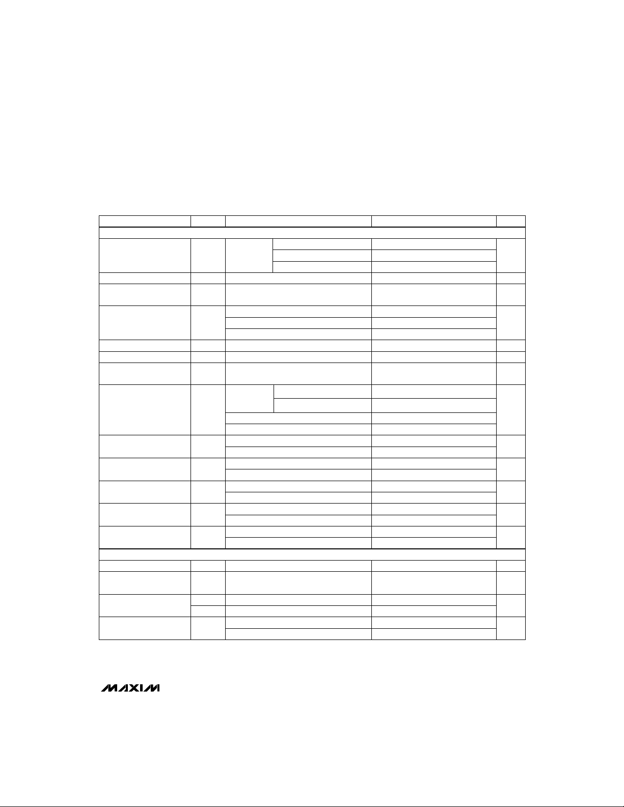
ELECTRICAL CHARACTERISTICS (continued)
(VCC= 4.6V to 5.5V for the MAX80_L, VCC= 4.5V to 5.5V for the MAX80_N, VCC= 4.35V to 5.5V for the MAX80_M; V
T
= T
to T
A
MIN
RESET AND LOW-LINE
Reset Threshold
LOWLINE to RESET
Threshold Voltage
LOWLINE Threshold,
Rising
V
CC
VCCto RESET Delay
VCCto LOWLINE Delay
RESET Active Timeout
Period
RESET Output Voltage
RESET Output
Short-Circuit Current
RESET Output Voltage
(MAX801)
RESET Output Short-
Circuit Current (MAX801)
LOWLINE Output Voltage
LOWLINE Output
Short-Circuit Current
WATCHDOG TIMER (MAX801)
Watchdog Timeout Period
Minimum Watchdog Input
Pulse Width
WDI Threshold Voltage
(Note 4)
WDI Input Current
. Typical values are at VCC= 5V and TA= +25°C, unless otherwise noted.)
MAX
CONDITIONS
VCCrising
V
RST
and falling
VCCfalling
LR
MAX80_L
MAX80_N
V
LL
MAX80_M
VCCfalling at 1mV/µs
RD
VCCfalling at 1mV/µs
LL
VCCrising
RP
I
SINK
V
BATT
VCCfalling
I
SINK
I
SOURCE
Output sink current, VCC= 4.25V
I
SC
Output source current
I
SINK
I
SOURCE
Output sink current
I
SC
Output source current, VCC= 4.25V
I
SINK
I
SOURCE
Output sink current, VCC= 4.25V
I
SC
Output source current
t
WD
VIL= 0.8V, VIH= 0.75V x V
V
IH
V
IL
RESET deasserted, WDI = 0V
RESET deasserted, WDI = V
MAX80_L
MAX80_N 4.500 4.575 4.650
MAX80_M
= 50µA,
= 3.2mA, VCC= 4.25V
= 3.2mA
= 3.2mA, VCC= 4.25V
VCC= 1.0V, MAX80_C
= 0V,
VCC= 1.2V, MAX80_E/M
= 0.1mA VCC- 1.5 VCC- 0.1
= 5mA, VCC= 4.25V
= 5mA, VCC= 4.25V
CC
CC
4.600 4.675 4.750
4.350 4.425 4.500
4.73 4.81
4.63 4.71
4.48 4.56
0.3
0.3
0.1 0.4
40
1.6
0.4
VCC- 1.5
55
15
0.4
VCC- 1.5
40
20
1.12 1.6 2.24 sec
100 ns
0.75 x V
CC
0.8
-50 -10
16 50
BATT
MAX801L/M/N, MAX808L/M/N
= 2.8V;
UNITSMIN TYP MAXSYMBOLPARAMETER
V
mV13Reset-Threshold Hysteresis
mV30 52 70V
V
µs17t
µs17t
ms140 200 280t
V
mA
V
mA
V
mA
V
µA
_______________________________________________________________________________________ 3

8-Pin µP Supervisory Circuits
with ±1.5% Reset Accuracy
ELECTRICAL CHARACTERISTICS (continued)
(VCC= 4.6V to 5.5V for the MAX80_L, VCC= 4.5V to 5.5V for the MAX80_N, VCC= 4.35V to 5.5V for the MAX80_M; V
T
= T
to T
A
MIN
CHIP-ENABLE GATING (MAX808)CHIP-ENABLE GATING (MAX808)
CE IN Leakage Current
CE IN to CE OUT
Resistance (Note 5)
CE OUT Short-Circuit
Current (RESET Active)
CE IN to CE OUT
Propagation Delay (Note 6)
CE OUT Output Voltage
High (RESET Active)
RESET to CE OUT Delay
(Note 7)
. Typical values are at VCC= 5V and TA= +25°C, unless otherwise noted.)
MAX
CONDITIONS
V
= 4.25V ±0.00002 ±1 µA
CC
Enabled mode, VCC= V
(max) Ω75 150
RST
VCC= 4.25V, CE OUT = 0V
VCC= 5V, C
50Ω source-impedance driver
VCC= 4.25V, I
VCC= 0V, I
= 50pF,
LOAD
= 2mA
OUT
= 10µA V
OUT
VCCfalling, CE IN = 0V
3.5
BATT
- 0.1 V
BATT
BATT
= 2.8V;
UNITSMIN TYP MAXSYMBOLPARAMETER
mA15
ns38
V
µs18
Note 1: Either VCCor V
Note 2: The supply current drawn by the MAX80_ from the battery (excluding I
< V
V
CC
BATT
Characteristics
can go to 0V if the other is greater than 2V.
BATT
. In most applications, this is a brief period as VCCfalls through this region (see
) typically goes to 15µA when (V
OUT
).
Typical Operating
BATT
- 0.1V) <
Note 3: “+” = battery-discharging current, “-” = battery-charging current.
Note 4: WDI is internally connected to a voltage divider between V
MAX801L/M/N, MAX808L/M/N
disabling the watchdog function.
Note 5: The chip-enable resistance is tested with V
Note 6: The chip-enable propagation delay is measured from the 50% point at CE IN to the 50% point at CE OUT.
CE IN
= V
and GND. If unconnected, WDI is typically driven to 1.8V,
CC
CC
/ 2 and I
CE IN
= 1mA.
Note 7: If CE IN goes high, CE OUT goes high immediately and stays high until reset is deasserted and CE IN is low.
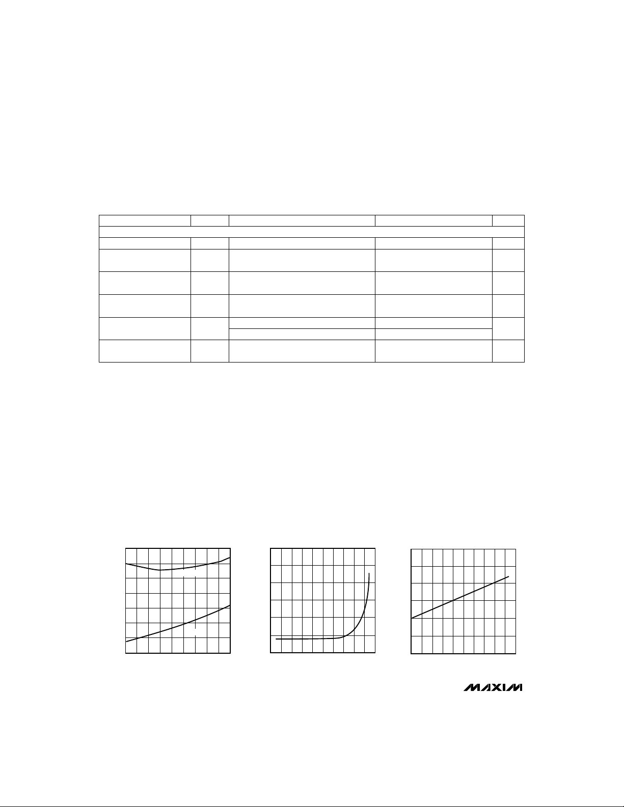
__________________________________________Typical Operating Characteristics
(VCC= 5V, V
VCC SUPPLY CURRENT vs. TEMPERATURE
75
70
65
60
55
SUPPLY CURRENT (µA)
50
CC
V
45
40
-55
= 2.8V, no load, TA= +25°C, unless otherwise noted.)
BATT
(NORMAL OPERATING MODE)
MAX801
MAX808
-15
-35 45 1255
TEMPERATURE (°C)
65
25
MAX801/808-01
105
85
TEMPERATURE (BATTERY-BACKUP MODE)
3.0
2.5
2.0
1.5
1.0
0.5
BATTERY SUPPLY CURRENT (µA)
0
-60 -20 60 140
BATTERY SUPPLY CURRENT vs.
20 100-40 40 120080
TEMPERATURE (°C)
CHIP-ENABLE PROPAGATION DELAY
MAX808
vs. TEMPERATURE
6
MAX801/808-02
5
4
3
2
PROPAGATION DELAY (ns)
1
0
-60 -20 60 140
20 100-40 40 120080
TEMPERATURE (°C)
MAX801/808-03
4 _______________________________________________________________________________________
 Loading...