

19-1086; Rev 0; 6/96
8-Pin µP Supervisory Circuits
with ±1.5% Reset Accuracy
_______________General Description
The MAX801/MAX808 microprocessor (µP) supervisory
circuits monitor and control the activities of +5V µPs by
providing backup-battery switchover, low-line indication, and µP reset. Additional features include a watchdog for the MAX801 and CMOS RAM write protection
for the MAX808.
The MAX801/MAX808 offer a choice of reset-threshold
voltage (denoted by suffix letter): 4.675V (L), 4.575V
(N), and 4.425V (M). These devices are available in
8-pin DIP and SO packages.
________________________Applications
Computers
Controllers
Intelligent Instruments
Critical µP Power Monitoring
Portable/Battery-Powered Equipment
Embedded Systems
Pin Configurations appear at end of data sheet.
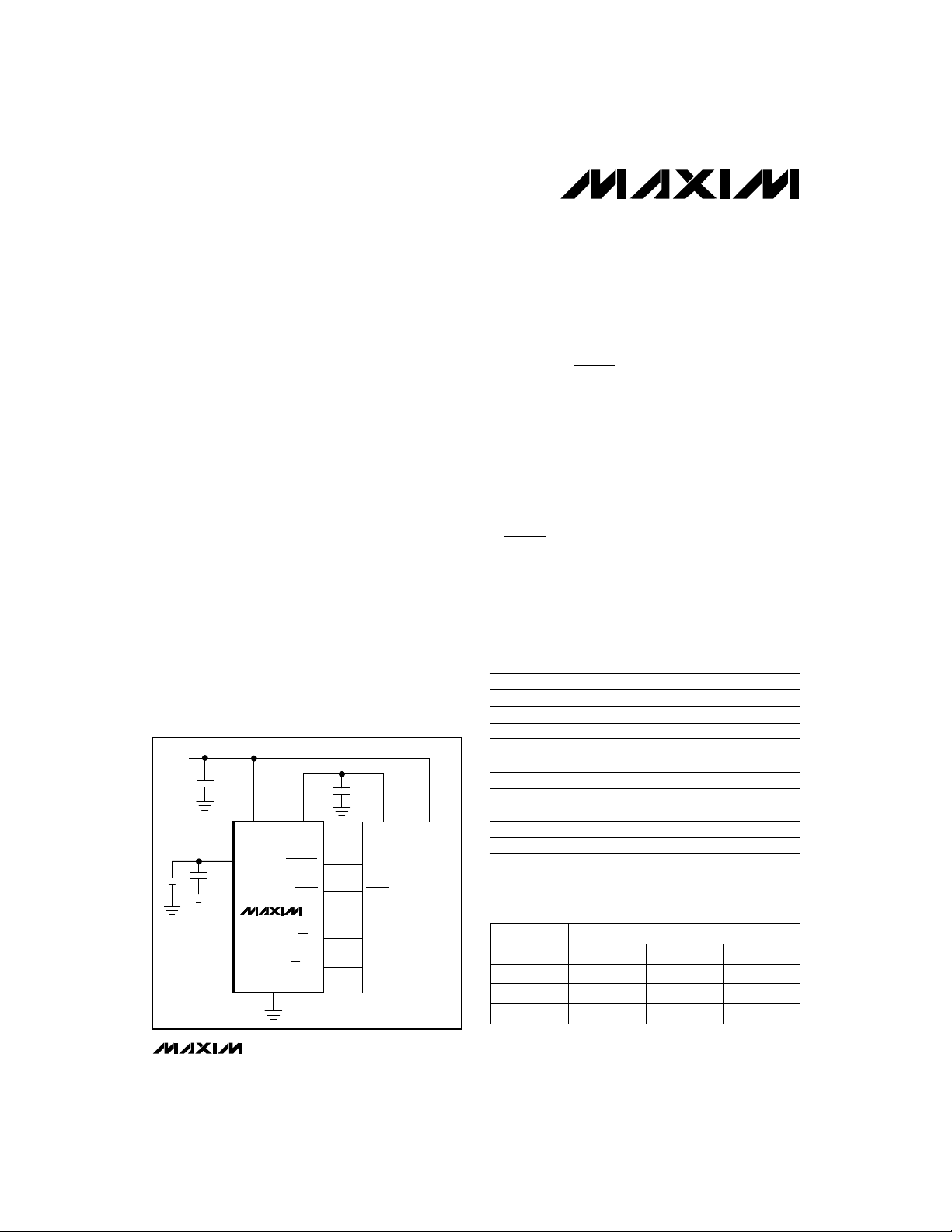
__________Typical Operating Circuit
+5V
0.1µF
0.1µF
BATT
V
CC
MAX808
OUT
LOWLINE
RESET
CE IN
CE OUT
GND
0.1µF
POWER FOR
CMOS RAM
NMI
RESET
µP SYSTEM
FROM I/O SYSTEM OR
ADDRESS DECODER
TO CMOS RAM
µP
POWER
____________________________Features
♦ Precision Voltage Monitoring, ±1.5% Reset
Accuracy
♦ 200ms Power-OK/Reset Time Delay
♦ RESET Output (MAX808)
RESET and RESET Outputs (MAX801)
♦ Watchdog Timer (MAX801)
♦ On-Board Gating of Chip-Enable Signals (MAX808):
Memory Write-Cycle Completion
3ns CE Gate Propagation Delay
♦ 1µA Standby Current
♦ Power Switching:
250mA in VCCMode
20mA in Battery-Backup Mode
♦ MaxCap™/SuperCap™ Compatible
♦ RESET Guaranteed Valid to VCC= 1V
♦ Low-Line Threshold 52mV Above Reset
Threshold
MaxCap is a trademark of The Carborundum Corp.
SuperCap is a trademark of Baknor Industries.
______________Ordering Information
PART*
MAX801_CPA
MAX801_CSA
MAX801_EPA -40°C to +85°C
MAX801_ESA
MAX801_MJA
MAX808_CPA
MAX808_CSA 0°C to +70°C 8 SO
MAX808_EPA
MAX808_ESA
MAX808_MJA -55°C to +125°C
* These parts offer a choice of reset threshold voltage. From the
table below, select the suffix corresponding to the desired
threshold and insert it into the blank to complete the part number.
**Contact factory for availability and processing to MIL-STD-883.
SUFFIX
L 4.60 4.675
N 4.50
M 4.35
TEMP. RANGE PIN-PACKAGE
0°C to +70°C
0°C to +70°C
-40°C to +85°C 8 SO
-55°C to +125°C
0°C to +70°C
-40°C to +85°C 8 Plastic DIP
-40°C to +85°C
RESET THRESHOLD (V)
MIN MAX
8 Plastic DIP
8 SO
8 Plastic DIP
8 CERDIP**
8 Plastic DIP
8 SO
8 CERDIP**
TYP
4.75
4.575 4.65
4.425 4.50
MAX801L/M/N, MAX808L/M/N
________________________________________________________________
Maxim Integrated Products
1
For free samples & the latest literature: http://www.maxim-ic.com, or phone 1-800-998-8800
8-Pin µP Supervisory Circuits
with ±1.5% Reset Accuracy
ABSOLUTE MAXIMUM RATINGS
Input Voltage (with respect to GND)
.......................................................................-0.3V to +6V
V
CC
....................................................................-0.3V to +6V
V
BATT
All Other Pins........................................-0.3V to (V
Input Current
Peak ..........................................................................1.0A
V
CC
Continuous ............................................................500mA
V
CC
Peak.....................................................................250mA
I
BATT
Continuous ............................................................50mA
I
BATT
GND................................................................................50mA
OUT
+ 0.3V)
All Other Inputs...............................................................50mA
Output Current
OUT Peak..........................................................................1.0A
Stresses beyond those listed under “Absolute Maximum Ratings” may cause permanent damage to the device. These are stress ratings only, and functional
operation of the device at these or any other conditions beyond those indicated in the operational sections of the specifications is not implied. Exposure to
absolute maximum rating conditions for extended periods may affect device reliability.
ELECTRICAL CHARACTERISTICS
(VCC= 4.6V to 5.5V for the MAX80_L, VCC= 4.5V to 5.5V for the MAX80_N, VCC= 4.35V to 5.5V for the MAX80_M; V
T
= T
to T
A
MIN
Operating Voltage Range
, BATT (Note 1)
V
CC
V
in Normal Operating
OUT
Mode
MAX801L/M/N, MAX808L/M/N
VCCto OUT
On-Resistance
V
in Battery-Backup
OUT
Mode
BATT to OUT
On-Resistance
Supply Current in Normal
Operating Mode
(excludes I
Supply Current in BatteryBackup Mode (excludes
I
) (Note 2)
OUT
BATT Standby Current
(Note 3)
Battery-Switchover
Threshold
Battery-Switchover
Hysteresis
. Typical values are at VCC= 5V and TA= +25°C, unless otherwise noted.)
MAX
CONDITIONS
I
= 25mA VCC- 0.02
OUT
I
VCC= 4.5V VCC- 0.38 VCC- 0.25
VCC= 3V, V
VCC= 4.5V,
I
= 250mA
OUT
VCC= 3V, I
VCC= 0V V
VCC= 0V Ω
= 250mA, MAX80_C/E
OUT
I
= 250mA, MAX80_M VCC- 0.45
OUT
= 2.8V, I
BATT
MAX80_C/E
MAX80_M
= 100mA
OUT
V
BATT
V
BATT
V
BATT
V
BATT
V
BATT
V
BATT
MAX801
OUT
)
MAX808
VCC= 0V,
V
= 2.8V
BATT
V
+ 0.2V
BATT
≤ V
CC
V
= 2.8V
BATT
TA= +25°C
TA= T
MIN
to T
MAX
TA= +25°C
TA= T
MIN
Power-up
Power-down
OUT Continuous............................................................500mA
All Other Outputs ............................................................50mA
Continuous Power Dissipation (T
Plastic DIP (derate 9.09mW/°C above +70°C) ............727mW
= +70°C)
A
SO (derate 5.88mW/°C above +70°C).........................471mW
CERDIP (derate 8.00mW/°C above +70°C).................640mW
Operating Temperature Ranges
MAX801_C_A/MAX808_C_A...............................0°C to +70°C
MAX801_E_A/MAX808_E_A ............................-40°C to +85°C
MAX801_MJA/MAX808_MJA.........................-55°C to +125°C
Storage Temperature Range.............................-65°C to +160°C
Lead Temperature (soldering, 10sec).............................+300°C
OUT
= 100mA
VCC- 0.25 VCC- 0.12
1.0 1.5
1.2 2.5
= 4.5V, I
= 2.8V, I
= 2.0V, I
= 4.5V, I
= 2.8V, I
= 2.0V, I
= 20mA V
OUT
= 10mA V
OUT
= 5mA
OUT
= 20mA 8
OUT
= 10mA 12 25
OUT
= 5mA
OUT
V
BATT
BATT
- 0.25 V
- 0.20 V
- 0.16
BATT
- 0.12
BATT
- 0.08
BATT
16 40
68 110
48 90
0.4 1
MAX80_C/E
MAX80_M
-0.1 0.1
to T
MAX
-1.0 1.0
V
+ 0.05
BATT
V
BATT
50 mV
BATT
1.8
5
50
= 2.8V;
UNITSMIN TYP MAXSYMBOLPARAMETER
V0 X 5.5
V
Ω
µA
µA
µA
V
2 _______________________________________________________________________________________
8-Pin µP Supervisory Circuits
with ±1.5% Reset Accuracy
ELECTRICAL CHARACTERISTICS (continued)
(VCC= 4.6V to 5.5V for the MAX80_L, VCC= 4.5V to 5.5V for the MAX80_N, VCC= 4.35V to 5.5V for the MAX80_M; V
T
= T
to T
A
MIN
RESET AND LOW-LINE
Reset Threshold
LOWLINE to RESET
Threshold Voltage
LOWLINE Threshold,
Rising
V
CC
VCCto RESET Delay
VCCto LOWLINE Delay
RESET Active Timeout
Period
RESET Output Voltage
RESET Output
Short-Circuit Current
RESET Output Voltage
(MAX801)
RESET Output Short-
Circuit Current (MAX801)
LOWLINE Output Voltage
LOWLINE Output
Short-Circuit Current
WATCHDOG TIMER (MAX801)
Watchdog Timeout Period
Minimum Watchdog Input
Pulse Width
WDI Threshold Voltage
(Note 4)
WDI Input Current
. Typical values are at VCC= 5V and TA= +25°C, unless otherwise noted.)
MAX
CONDITIONS
VCCrising
V
RST
and falling
VCCfalling
LR
MAX80_L
MAX80_N
V
LL
MAX80_M
VCCfalling at 1mV/µs
RD
VCCfalling at 1mV/µs
LL
VCCrising
RP
I
SINK
V
BATT
VCCfalling
I
SINK
I
SOURCE
Output sink current, VCC= 4.25V
I
SC
Output source current
I
SINK
I
SOURCE
Output sink current
I
SC
Output source current, VCC= 4.25V
I
SINK
I
SOURCE
Output sink current, VCC= 4.25V
I
SC
Output source current
t
WD
VIL= 0.8V, VIH= 0.75V x V
V
IH
V
IL
RESET deasserted, WDI = 0V
RESET deasserted, WDI = V
MAX80_L
MAX80_N 4.500 4.575 4.650
MAX80_M
= 50µA,
= 3.2mA, VCC= 4.25V
= 3.2mA
= 3.2mA, VCC= 4.25V
VCC= 1.0V, MAX80_C
= 0V,
VCC= 1.2V, MAX80_E/M
= 0.1mA VCC- 1.5 VCC- 0.1
= 5mA, VCC= 4.25V
= 5mA, VCC= 4.25V
CC
CC
4.600 4.675 4.750
4.350 4.425 4.500
4.73 4.81
4.63 4.71
4.48 4.56
0.3
0.3
0.1 0.4
40
1.6
0.4
VCC- 1.5
55
15
0.4
VCC- 1.5
40
20
1.12 1.6 2.24 sec
100 ns
0.75 x V
CC
0.8
-50 -10
16 50
BATT
MAX801L/M/N, MAX808L/M/N
= 2.8V;
UNITSMIN TYP MAXSYMBOLPARAMETER
V
mV13Reset-Threshold Hysteresis
mV30 52 70V
V
µs17t
µs17t
ms140 200 280t
V
mA
V
mA
V
mA
V
µA
_______________________________________________________________________________________ 3
8-Pin µP Supervisory Circuits
with ±1.5% Reset Accuracy
ELECTRICAL CHARACTERISTICS (continued)
(VCC= 4.6V to 5.5V for the MAX80_L, VCC= 4.5V to 5.5V for the MAX80_N, VCC= 4.35V to 5.5V for the MAX80_M; V
T
= T
to T
A
MIN
CHIP-ENABLE GATING (MAX808)CHIP-ENABLE GATING (MAX808)
CE IN Leakage Current
CE IN to CE OUT
Resistance (Note 5)
CE OUT Short-Circuit
Current (RESET Active)
CE IN to CE OUT
Propagation Delay (Note 6)
CE OUT Output Voltage
High (RESET Active)
RESET to CE OUT Delay
(Note 7)
. Typical values are at VCC= 5V and TA= +25°C, unless otherwise noted.)
MAX
CONDITIONS
V
= 4.25V ±0.00002 ±1 µA
CC
Enabled mode, VCC= V
(max) Ω75 150
RST
VCC= 4.25V, CE OUT = 0V
VCC= 5V, C
50Ω source-impedance driver
VCC= 4.25V, I
VCC= 0V, I
= 50pF,
LOAD
= 2mA
OUT
= 10µA V
OUT
VCCfalling, CE IN = 0V
3.5
BATT
- 0.1 V
BATT
BATT
= 2.8V;
UNITSMIN TYP MAXSYMBOLPARAMETER
mA15
ns38
V
µs18
Note 1: Either VCCor V
Note 2: The supply current drawn by the MAX80_ from the battery (excluding I
< V
V
CC
BATT
Characteristics
can go to 0V if the other is greater than 2V.
BATT
. In most applications, this is a brief period as VCCfalls through this region (see
) typically goes to 15µA when (V
OUT
).
Typical Operating
BATT
- 0.1V) <
Note 3: “+” = battery-discharging current, “-” = battery-charging current.
Note 4: WDI is internally connected to a voltage divider between V
MAX801L/M/N, MAX808L/M/N
disabling the watchdog function.
Note 5: The chip-enable resistance is tested with V
Note 6: The chip-enable propagation delay is measured from the 50% point at CE IN to the 50% point at CE OUT.
CE IN
= V
and GND. If unconnected, WDI is typically driven to 1.8V,
CC
CC
/ 2 and I
CE IN
= 1mA.
Note 7: If CE IN goes high, CE OUT goes high immediately and stays high until reset is deasserted and CE IN is low.
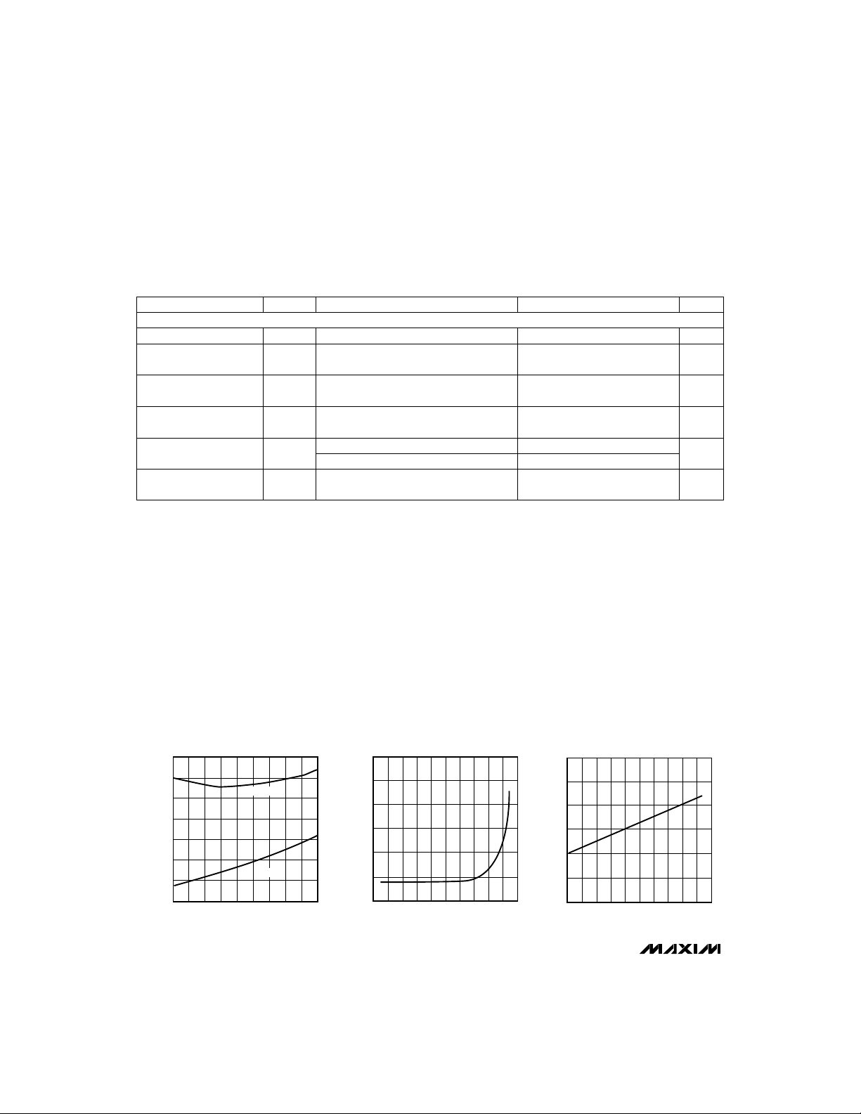
__________________________________________Typical Operating Characteristics
(VCC= 5V, V
VCC SUPPLY CURRENT vs. TEMPERATURE
75
70
65
60
55
SUPPLY CURRENT (µA)
50
CC
V
45
40
-55
= 2.8V, no load, TA= +25°C, unless otherwise noted.)
BATT
(NORMAL OPERATING MODE)
MAX801
MAX808
-15
-35 45 1255
TEMPERATURE (°C)
65
25
MAX801/808-01
105
85
TEMPERATURE (BATTERY-BACKUP MODE)
3.0
2.5
2.0
1.5
1.0
0.5
BATTERY SUPPLY CURRENT (µA)
0
-60 -20 60 140
BATTERY SUPPLY CURRENT vs.
20 100-40 40 120080
TEMPERATURE (°C)
CHIP-ENABLE PROPAGATION DELAY
MAX808
vs. TEMPERATURE
6
MAX801/808-02
5
4
3
2
PROPAGATION DELAY (ns)
1
0
-60 -20 60 140
20 100-40 40 120080
TEMPERATURE (°C)
MAX801/808-03
4 _______________________________________________________________________________________

8-Pin µP Supervisory Circuits
with ±1.5% Reset Accuracy
____________________________Typical Operating Characteristics (continued)
(VCC= 5V, V
8
6
4
2
PROPAGATION DELAY (ns)
0
0 50 100
4.70
4.65
4.60
4.55
4.50
RESET THRESHOLD (V)
4.45
4.40
-60 -20 60 140
4.80
4.75
4.70
4.65
4.60
4.55
4.50
LOWLINE THRESHOLD (V)
4.45
4.40
-60 -20 60 140
= 2.8V, no load, TA= +25°C, unless otherwise noted.)
BATT
MAX808
CHIP-ENABLE PROPAGATION DELAY
vs. CE OUT LOAD CAPACITANCE
50Ω DRIVER
C
(pF)
LOAD
RESET THRESHOLD
vs. TEMPERATURE
MAX80_L
MAX80_N
MAX80_M
20 100-40 40 120080
TEMPERATURE (°C)
LOWLINE THRESHOLD
vs. TEMPERATURE (V
20 100-40 40 120080
TEMPERATURE (°C)
RISING)
CC
MAX80_L
MAX80_N
MAX80_M
30
MAX801/808-04
25
20
ON-RESISTANCE (Ω)
15
OUT
TO V
10
BATT
V
5
280
260
MAX801/808-07
240
220
200
180
RESET TIMEOUT PERIOD (ms)
160
140
40
35
MAX801/808-10
30
25
20
15
10
PROPAGATION DELAY (µs)
5
0
BATT to OUT ON-RESISTANCE
vs. TEMPERATURE
V
= 0V
CC
= 10mA
I
OUT
V
= 2.0V
BATT
V
= 2.8V
BATT
V
= 4.5V
BATT
-60 -20 60 140
vs. TEMPERATURE (V
-60 -20 60 140
LOWLINE COMPARATOR PROPAGATION
DELAY vs. TEMPERATURE (V
V
CC
-60 -20 60 140
20 100-40 40 120080
TEMPERATURE (°C)
RESET TIMEOUT PERIOD
20 100-40 40 120080
TEMPERATURE (°C)
FALLING AT 1mV/µs
20 100-40 40 120080
TEMPERATURE (°C)
CC
RISING)
FALLING)
CC
V
to OUT ON-RESISTANCE
CC
1.6
1.5
MAX801/808-05
1.4
1.3
1.2
1.1
ON-RESISTANCE (Ω)
OUT
1.0
TO V
0.9
CC
V
0.8
0.7
80
70
MAX801/808-08
60
50
40
30
20
10
LOWLINE TO RESET THRESHOLD (mV)
0
40
35
MAX801/808-11
30
25
20
15
10
PROPAGATION DELAY (µs)
5
0
vs. TEMPERATURE
I
= 250mA
OUT
-60 -20 60 140
vs. TEMPERATURE (V
-60 -20 60 140
RESET COMPARATOR PROPAGATION
DELAY vs. TEMPERATURE (V
V
-60 -20 60 140
20 100-40 40 120080
TEMPERATURE (°C)
LOWLINE to RESET THRESHOLD
20 100-40 40 120080
TEMPERATURE (°C)
FALLING AT 1mV/µs
CC
20 100-40 40 120080
TEMPERATURE (°C)
FALLING)
CC
FALLING)
CC
MAX801L/M/N, MAX808L/M/N
MAX801/808-06
MAX801/808-09
MAX801/808-12
_______________________________________________________________________________________
5

8-Pin µP Supervisory Circuits
with ±1.5% Reset Accuracy
____________________________Typical Operating Characteristics (continued)
(VCC= 5V, V
MAX801L/M/N, MAX808L/M/N
= 2.8V, no load, TA= +25°C, unless otherwise noted.)
BATT
BATTERY CURRENT
vs. INPUT SUPPLY VOLTAGE
16
14
12
10
8
6
4
BATTERY CURRENT (µA)
2
0
2.5 2.6 2.7 2.8 2.9 3.0
1000
SLOPE = 1.0Ω
100
VOLTAGE (mV)
OUT
10
TO V
CC
V
1
1 10010 1000
VCC (V)
V
to OUT VOLTAGE vs.
CC
OUTPUT CURRENT
I
OUT
(mA)
MAX801/808-13
MAX801/808-15
BATT to OUT VOLTAGE vs.
1000
VOLTAGE (mV)
100
OUT
TO V
BATT
V
10
1000
100
10
MAXIMUM TRANSIENT DURATION (µs)
1
OUTPUT CURRENT
V
= 0V
CC
SLOPE = 12Ω
1 10 100
MAXIMUM TRANSIENT DURATION vs.
RESET THRESHOLD OVERDRIVE
1 10010 1000
RESET THRESHOLD OVERDRIVE (mV)
I
(mA)
OUT
RESET OCCURS
MAX801/808-14
MAX801/808-16
______________________________________________________________Pin Description
PIN
MAX801 MAX808
22
33
6 _______________________________________________________________________________________
NAME
V
CC
LOWLINE
RESET
GND Ground44
FUNCTION
Input Supply Voltage, nominally +5V. Bypass with a 0.1µF capacitor to GND.11
Low-Line Comparator Output. This CMOS-logic output goes low when VCCfalls to 52mV
above the reset threshold. Use LOWLINE to generate an NMI, initiating an orderly shutdown routine when V
is falling. LOWLINE swings between VCCand GND.
CC
Active-Low Reset Output. RESET is triggered and stays low when VCCis below the reset
threshold (or during a watchdog timeout for the MAX801). It remains low 200ms after
V
rises above the reset threshold (or 200ms after the watchdog timeout occurs).
CC
RESET has a strong pull-down but a relatively weak pull-up, and can be wire-OR connected to logic gates. Valid for V
≥ 1V. RESET swings between VCCand GND.
CC

8-Pin µP Supervisory Circuits
with ±1.5% Reset Accuracy
_________________________________________________Pin Description (continued)
PIN
MAX801 MAX808
—5
5—
—6
77
88
V
CC
BATT
GND
NAME
RESET
CE OUT
WDI
CE IN
BATT
OUT
2.275V
FUNCTION
Active-High Reset Output. RESET is the inverse of RESET. It is a CMOS output that
sources and sinks current. RESET swings between V
and GND.
CC
Chip-Enable Output. Output to the chip-enable gating circuit. CE OUT is pulled up to
the higher of V
CC
or V
when the chip-enable gate is disabled.
BATT
Watchdog Input. If WDI remains high or low longer than the watchdog timeout period
(typically 1.6sec), RESET will be asserted for 200ms. Leave unconnected to disable the
watchdog function.
Chip-Enable Input6—
Backup-Battery Input. When VCCfalls below the reset threshold and V
es from VCCto BATT. V
MAX801/MAX808 is powered up, provided BATT is bypassed with a 0.1µF capacitor to
may exceed VCC. The battery can be removed while the
BATT
BATT
GND. If no battery is used, connect BATT to ground and VCCto OUT.
Output Supply Voltage to CMOS RAM. When VCCexceeds the reset threshold or V
OUT connects to VCC. When VCCfalls below the reset threshold and V
nects to BATT. Bypass OUT with a 0.1µF capacitor to GND.
BATTERY-BACKUP
COMPARATOR
RESET
COMPARATOR
LOW-LINE
COMPARATOR
OSCILLATOR
MAX801
MAX808
WATCHDOG
TRANSITION
DETECTOR
STATE
MACHINE
THE HIGHER
OF V
OR V
BATT
CC
BATT
OUT
LOWLINE
MAX801 ONLY
WDI
RESET (MAX801 ONLY)
RESET
MAX808 ONLY
, OUT switch-
BATT
, OUT con-
,
MAX801L/M/N, MAX808L/M/N
CE IN
Figure 1. Functional Diagram
_______________________________________________________________________________________ 7
P
P
CE OUT
N

8-Pin µP Supervisory Circuits
with ±1.5% Reset Accuracy
V
RSTVLL
V
CC
V
LOWLINE
V
RESET
V
RESET
(MAX801)
V
CE OUT
(MAX808)
V
BATT
SHOWN FOR V
= 0V to 5V, V
CC
t
RP
t
RP
= 2.8V, CE IN = GND
BATT
Figure 2a. Timing Diagram, VCCRising
_______________Detailed Description
The MAX801/MAX808 microprocessor (µP) supervisory
MAX801L/M/N, MAX808L/M/N
circuits provide power-supply monitoring and backupbattery switchover in µP systems. The MAX801 also
provides program-execution watchdog functions
(Figure 1). Use of BiCMOS technology results in an
improved, 1.5% reset-threshold precision while keeping
supply currents typically at 68µA (48µA for the
V
(MAX801)
(MAX808)
Figure 2b. Timing Diagram, VCCFalling
The RESET output is active low, and is implemented with
a strong pull-down/relatively weak pull-up structure. It is
guaranteed to be a logic low for 0V < VCC< V
vided V
tery, RESET is guaranteed valid for VCC≥ 1V.
The RESET output is the inverse of the RESET output; it
both sources and sinks current and cannot be wire-OR
connected.
MAX808). The MAX801/MAX808 are intended for battery-powered applications that require high resetthreshold precision, allowing a wide power-supply
operating range while preventing the system from operating below its specified voltage range.
RESET
and RESET Outputs
The MAX801/MAX808’s RESET output ensures that the
µP powers up in a known state, and prevents codeexecution errors during power-down and brownout
conditions. It does this by resetting the µP, terminating
program execution when VCCdips below the reset
threshold. Each time RESET is asserted, it stays low for
at least the 200ms reset timeout period (set by an internal timer) to ensure the µP has adequate time to return
to an initial state. The internal timer restarts any time
VCCgoes below the reset threshold (V
) before the
RST
reset timeout period is completed. The watchdog timer
on the MAX801 can also initiate a reset (see the
MAX801 Watchdog Timer
section).
The low-line comparator monitors VCCwith a threshold
voltage typically 52mV above the reset threshold, with
13mV of hysteresis. Use LOWLINE to provide a nonmaskable interrupt (NMI) to the µP when power begins
to fall, initiating an orderly software shutdown routine. In
most battery-operated portable systems, reserve energy in the battery provides ample time to complete the
shutdown routine once the low-line warning is encountered and before reset asserts. If the system must contend with a more rapid VCCfall time (such as when the
main battery is disconnected, when a DC-DC converter
shuts down, or when a high-side switch is opened during normal operation), use capacitance on the VCCline
to provide time to execute the shutdown routine (Figure
3). First calculate the worst-case time required for the
system to perform its shutdown routine. Then, with
worst-case shutdown time, worst-case load current,
and minimum low-line to reset threshold (V
V
LOWLINE
V
RESET
V
RESET
V
CE OUT
V
V
+ V
RST
RST
LR
CC
t
LL
t
RD
t
RD
t
RCE
SHOWN FOR V
is greater than 2V. Without a backup bat-
BATT
= 5V to 0V, V
CC
V
BATT
= 2.8V, CE IN = GND
BATT
Low-Line Comparator
, pro-
RST
LR(min)
),
8 _______________________________________________________________________________________

8-Pin µP Supervisory Circuits
with ±1.5% Reset Accuracy
MAX801L/M/N, MAX808L/M/N
HOLD
> I
C
LOAD
4.5V to 5.5V
HOLD
x t
SHDN
LR
LOWLINE
V
CC
MAX801
MAX808
GND
TO µP NMI
REGULATOR
C
V
Figure 3. Using LOWLINE to Provide a Power-Fail Warning to
the µP
calculate the amount of capacitance required to allow
the shutdown routine to complete before reset is
asserted:
C
where t
= (I
HOLD
is the time required for the system to com-
SHDN
LOAD
x t
SHDN
) / (V
LR(min)
)
plete the shutdown routine (including the VCCto lowline propagation delay), I
is the current being
LOAD
drained from the capacitor, and VLRis the low-line to
reset threshold.
Output Supply Voltage
The output supply (OUT) transfers power from VCCor
BATT to the µP, RAM, and other external circuitry. At
the maximum source current of 250mA, V
OUT
will typically be 220mV below VCC. Decouple OUT with a 0.1µF
capacitor to ground.
Battery-Backup Mode
Battery-backup mode preserves the contents of RAM in
the event of a brownout or power failure. With a backup
battery installed at BATT, the MAX801/MAX808 automatically switches RAM to backup power when VCCfalls.
Two conditions are required for switchover to batterybackup mode: 1) VCCmust be below the reset threshold;
2) VCCmust be below V
. Table 1 lists the status of
BATT
inputs and outputs during battery-backup mode.
BATT is designed to conduct up to 20mA to OUT dur-
ing battery backup. The PMOS switch on-resistance is
approximately 12Ω. Figure 4 shows the two series pass
elements (between the BATT input and OUT) that
facilitate UL recognition. V
can exceed VCCduring
BATT
normal operation without causing a reset.
MAX801
MAX808
V
CC
CONTROL
CIRCUITRY
BATT
Figure 4. VCCand BATT to OUT Switch
P
PP
Table 1. Input and Output Status in
Battery-Backup Mode
PIN
MAX801 MAX808
5
NAME
Battery switchover
V
11
LOWLINE
RESET
GND
44
RESET
—
5—
CE OUT
—6
CE IN
BATT
77
OUT
88
comparator monitors V
CC
for active switchover.
Logic low22
Logic low33
Ground—0V reference for
all signals
Logic high; the open-circuit
voltage is equal to VCC.
Logic high. The open-circuit
output voltage is equal to
V
WDI is ignored and goes
WDI
high impedance.
High impedance (MAX808)6—
Supply current is 1µA max for
V
OUT is connected to BATT
through two internal PMOS
switches in series.
BATT
BATT
STATUS
(MAX808).
≤ 2.8V.
OUT
0.1µF
CC
_______________________________________________________________________________________ 9

8-Pin µP Supervisory Circuits
with ±1.5% Reset Accuracy
The watchdog monitors the µP’s activity. If the µP does
MAX801 Watchdog Timer
not toggle the watchdog input (WDI) within 1.6sec,
reset asserts for the reset timeout period. The internal
1.6sec timer is cleared when reset asserts or when a
transition (low-to-high or high-to-low) occurs at WDI
V
CC
while reset is not asserted. The timer remains cleared
and does not count as long as reset is asserted. It
starts counting as soon as reset is released (Figure 5).
RESET
Supply current is typically reduced by 10µA when WDI
is at a valid logic level. To disable the watchdog function, leave WDI unconnected. An internal voltage
divider sets WDI to about mid-supply, disabling the
WDI
watchdog timer/counter.
MAX808 Chip-Enable Gating
The MAX808 provides internal gating of chip-enable
(CE) signals to prevent erroneous data from corrupting
Figure 5. Watchdog Timing
CMOS RAM in the event of a power failure. During normal operation, the CE gate is enabled and passes all
CE transitions. When reset is asserted, this path
becomes disabled, preventing erroneous data from
corrupting the CMOS RAM. The MAX808 uses a series
transmission gate from the chip-enable input (CE IN) to
THRESHOLD
the chip-enable output (CE OUT) (Figure 1). The 8ns
max chip-enable propagation from CE IN to CE OUT
enables the MAX808 to be used with most µPs.
The MAX808 also features write-cycle-completion cir-
MAX801L/M/N, MAX808L/M/N
cuitry. If VCCfalls below the reset threshold while the
CE OUT
µP is writing to RAM, the MAX808 holds the CE gate
enabled for 18µs to allow the µP to complete the write
instruction. If the write cycle has not completed by the
end of the 18µs period, the CE transmission gate turns
off and CE OUT goes high. If the µP completes the
write instruction during the 18µs period, the CE gate
turns off (high impedance) and CE OUT goes high as
soon as the µP pulls CE IN high. CE OUT remains high,
even if CE IN falls low for any reason (Figure 6).
Chip-Enable Input
CE IN is high impedance (disabled mode) while reset is
asserted. During a power-down sequence when V
passes the reset threshold, the CE transmission gate
disables. CE IN becomes high impedance 18µs after
reset asserts, provided CE IN is still low. If the µP completes the write instruction during the 18µs period, the
CE gate turns off. CE IN becomes high impedance as
soon as the µP pulls CE IN high. CE IN remains high
impedance even if the signal at CE IN falls low (Figure
6). During a power-up sequence, CE IN remains high
impedance (regardless of CE IN activity) until reset is
deasserted following the reset timeout period.
Figure 6. Chip-Enable Timing
In high-impedance mode, the leakage currents into this
input are ±1µA max over temperature. In low-impedance mode, the impedance of CE IN appears as a 75Ω
resistor in series with the load at CE OUT.
CC
The propagation delay through the CE transmission
gate depends on both the source impedance of the
drive to CE IN and the capacitive loading on CE OUT
(see the Chip-Enable Propagation Delay vs. CE OUT
Load Capacitance graph in the
Characteristics
tion tested from the 50% point on CE IN to the 50%
point on CE OUT using a 50Ω driver and 50pF of load
capacitance (Figure 7). For minimum propagation
delay, minimize the capacitive load at CE OUT and use
a low-output-impedance driver.
V
RESET
CE IN
RESET
t
RP
CC
t
WD
t
RP
18µs18µs
17µs
Typical Operating
). The CE propagation delay is produc-
17µs
10 ______________________________________________________________________________________

8-Pin µP Supervisory Circuits
with ±1.5% Reset Accuracy
MAX801L/M/N, MAX808L/M/N
V
(max)
RST
V
CC
+5V
1N4148
V
CC
MAX808
CE IN
50Ω DRIVER
Figure 7. MAX808 CE Gate Test Circuit
GND
CE OUT
50pF C
LOAD
Chip-Enable Output
In enabled mode, CE OUT’s impedance is equivalent to
75Ω in series with the source driving CE IN. In disabled
mode, the 75Ω transmission gate is off and CE OUT is
actively pulled to the higher of VCCor V
BATT
. The
source turns off when the transmission gate is enabled.
__________Applications Information
The MAX801/MAX808 are not short-circuit protected.
Shorting OUT to ground, other than power-up transients
such as charging a decoupling capacitor, may destroy
the device. If long leads connect to the IC’s inputs,
ensure that these lines are free from ringing and other
conditions that would forward bias the IC’s protection
diodes. Bypass OUT, VCC, and BATT with 0.1µF
capacitors to GND.
The MAX801/MAX808 operate in two distinct modes:
1) Normal Operating Mode, with all circuitry powered
up. Typical supply current from V
for the MAX808), while only leakage currents flow
from the battery.
2) Battery-Backup Mode, where V
and V
. The supply current from the battery is typ-
RST
ically less than 1µA.
Using SuperCaps™ or MaxCaps™
with the MAX801/MAX808
BATT has the same operating voltage range as VCC, and
the battery-switchover threshold voltage is typically
V
when VCCis decreasing or V
BATT
VCCis increasing. This hysteresis allows use of a
SuperCap (e.g., around 0.47F) and a simple charging
is 68µA (48µA
CC
is below V
CC
+ 0.05V when
BATT
BATT
BATT OUT
0.47F
MAX801
MAX808
GND
Figure 8. Using the MAX801/MAX808 with a SuperCap
circuit as a backup source (Figure 8). Since V
BATT
can
exceed VCCwhile VCCis above the reset threshold, no
special precautions are needed when using these µP
supervisors with a SuperCap.
Backup-Battery Replacement
The backup battery can be disconnected while VCCis
above the reset threshold, provided BATT is bypassed
with a 0.1µF capacitor to ground. No precautions are
necessary to avoid spurious reset pulses.
Negative-Going VCCTransients
While issuing resets to the µP during power-up, powerdown, and brownout conditions, these supervisors are
relatively immune to short-duration, negative-going V
CC
transients (glitches). It is usually undesirable to reset
the µP when VCCexperiences only small glitches.
The
Typical Operating Characteristics
show a graph of
Maximum Transient Duration vs. Reset Threshold
Overdrive, for which reset pulses are not generated.
The graph was produced using negative-going V
CC
pulses, starting at 5V and ending below the reset
threshold by the magnitude indicated (reset comparator overdrive). The graph shows the maximum pulse
width that a negative-going VCCtransient may typically
have without causing a reset pulse to be issued. As the
amplitude of the transient increases (i.e., goes farther
below the reset threshold), the maximum allowable
pulse width decreases. Typically, a VCCtransient that
goes 40mV below the reset threshold and lasts for 3µs
or less will not cause a reset pulse to be issued. A
0.1µF bypass capacitor mounted close to the VCCpin
provides additional transient immunity.
______________________________________________________________________________________ 11

8-Pin µP Supervisory Circuits
with ±1.5% Reset Accuracy
To help the watchdog timer keep a closer watch on
Watchdog Software Considerations
software execution, you can set and reset the watchdog input at different points in the program, rather than
“pulsing” the watchdog input high-low-high or low-highlow. This technique avoids a “stuck” loop, where the
watchdog timer continues to be reset within the loop,
keeping the watchdog from timing out.
Figure 9 shows a sample flow diagram where the I/O
driving the watchdog input is set high at the beginning
of the program, low at the beginning of every subroutine or loop, then high again when the program returns
to the beginning. If the program should “hang” in any
subroutine, the I/O would be continually set low and the
watchdog timer would be allowed to time out, causing a
reset or interrupt to be issued.
Maximum VCCFall Time
The VCCfall time is limited by the propagation delay of
the battery switchover comparator and should not
exceed 0.03V/µs. A standard rule for filter capacitance
on most regulators is around 100µF per Ampere of current. When the power supply is shut off or the main battery is disconnected, the associated initial VCCfall rate
Figure 9. Watchdog Flow Diagram
is just the inverse, or 1A/100µF = 0.01V/µs.
_________________Pin Configurations
MAX801L/M/N, MAX808L/M/N
TOP VIEW
V
LOWLINE
RESET
GND
1
CC
2
MAX801
3
4
8
OUT
BATT
7
WDI
6
RESET
5
___________________Chip Information
TRANSISTOR COUNT: 922
START
SET
WDI
LOW
SUBROUTINE
OR PROGRAM LOOP,
SET WDI
HIGH
RETURN
END
DIP/SO
1
V
CC
2
LOWLINE
RESET
GND
Maxim cannot assume responsibility for use of any circuitry other than circuitry entirely embodied in a Maxim product. No circuit patent licenses are
implied. Maxim reserves the right to change the circuitry and specifications without notice at any time.
12
__________________Maxim Integrated Products, 120 San Gabriel Drive, Sunnyvale, CA 94086 (408) 737-7600
© 1996 Maxim Integrated Products Printed USA is a registered trademark of Maxim Integrated Products.
MAX808
3
4
DIP/SO
8
OUT
BATT
7
CE IN
6
CE OUT
5
 Loading...