19-1175; Rev 0; 12/96
with Synchronous Rectifier for CPU Power
High-Accuracy Step-Down Controller
_______________General Description
The MAX798†high-performance, step-down DC-DC
converter provides main CPU power in battery-powered
systems. This buck controller achieves 96% efficiency
by using synchronous rectification and Maxim’s proprietary Idle Mode™ control scheme to extend battery life
at full-load (up to 10A) and no-load outputs. The
MAX798’s high accuracy meets the demanding requirements of the latest-generation CPUs. Excellent dynamic
response corrects output transients caused by the latest
dynamic-clock CPUs within five 300kHz clock cycles.
Unique bootstrap circuitry drives inexpensive N-channel
MOSFETs, reducing system cost and eliminating the crowbar switching currents found in some PMOS/NMOS switch
designs.
The MAX798 has a logic-controlled and synchronizable
fixed-frequency pulse-width-modulating (PWM) operating
mode, which reduces noise and RF interference in sensitive mobile-communications and pen-entry applications.
The SKIP override input allows automatic switchover to
idle-mode operation (for high-efficiency pulse skipping) at
light loads, or forces fixed-frequency mode for lowest noise
at all loads.
________________________Applications
____________________________Features
♦ 96% Efficiency
♦ 4.5V to 30V Input Range
♦ 1.6V to 6V Adjustable Precision Output
♦ ±0.4% Max Total Load-Regulation Error
♦ 0.06%/V Max Line-Regulation Error
♦ 5V Linear-Regulator Output
♦ Precision 2.505V Reference Output
♦ Automatic Bootstrap Circuit
♦ 150kHz/300kHz Fixed-Frequency PWM Operation
♦ Programmable Soft-Start
♦ 1.2mA Typical Quiescent Current
(VIN= 12V, V
OUT
= 2.5V)
♦ 1µA Typical Shutdown Current
______________Ordering Information
PIN-PACKAGETEMP. RANGEPART
16 Narrow SO-40°C to +85°CMAX798ESE
MAX798
Notebook and Subnotebook Computers
PDAs and Mobile Communicators
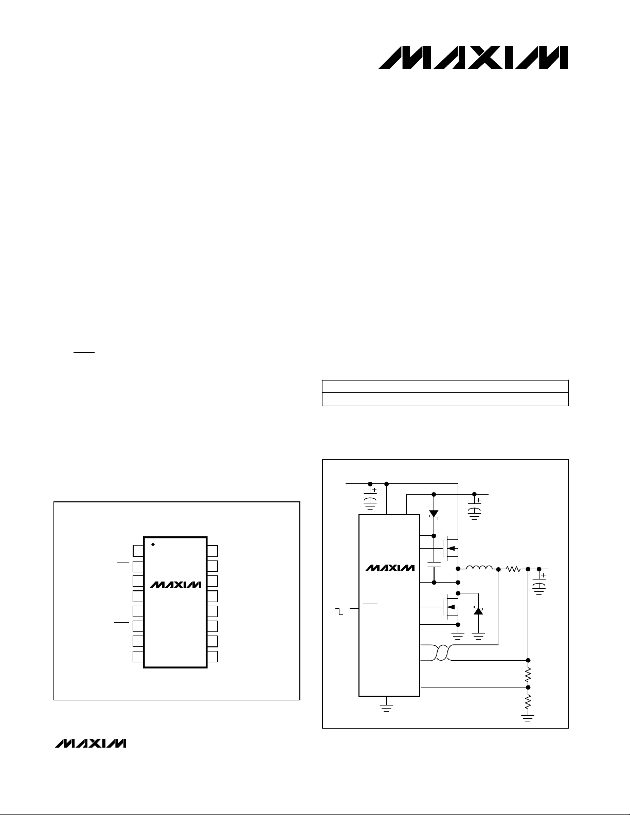
__________________Pin Configuration
TOP VIEW
SS
1
2
SKIP
REF
3
GND
SYNC
SHDN
FB
CSH
Idle Mode is a trademark of Maxim Integrated Products.
†
U.S. and foreign patents pending.
MAX798
4
5
6
7
8
SO
DH
16
LX
15
BST
14
DL
13
PGND
12
VL
11
V+
10
9
CSL
__________Typical Operating Circuit
INPUT
4.5V TO 30V
5V, 25mA
4.7µF
V+ VL
BST
DH
MAX798
ON
OFF
SHDN
GND
LX
DL
PGND
CSH
CSL
FB
0.1µF
N
R
SENSE
N
V
OUT
________________________________________________________________
Maxim Integrated Products
1
For free samples & the latest literature: http://www.maxim-ic.com, or phone 1-800-998-8800

High-Accuracy Step-Down Controller
with Synchronous Rectifier for CPU Power
ABSOLUTE MAXIMUM RATINGS
V+ to GND.................................................................-0.3V, +36V
GND to PGND........................................................................±2V
VL to GND ...................................................................-0.3V, +7V
BST to GND...............................................................-0.3V, +36V
DH to LX........................................................-0.3V, (BST + 0.3V)
LX to BST.....................................................................-7V, +0.3V
SHDN to GND............................................................-0.3V, +36V
MAX798
SYNC, SS, REF, SKIP, DL to GND...................-0.3V, (VL + 0.3V)
CSH, CSL to GND .......................................................-0.3V, +7V
VL Short Circuit to GND..............................................Momentary
Stresses beyond those listed under “Absolute Maximum Ratings” may cause permanent damage to the device. These are stress ratings only, and functional
operation of the device at these or any other conditions beyond those indicated in the operational sections of the specifications is not implied. Exposure to
absolute maximum rating conditions for extended periods may affect device reliability.
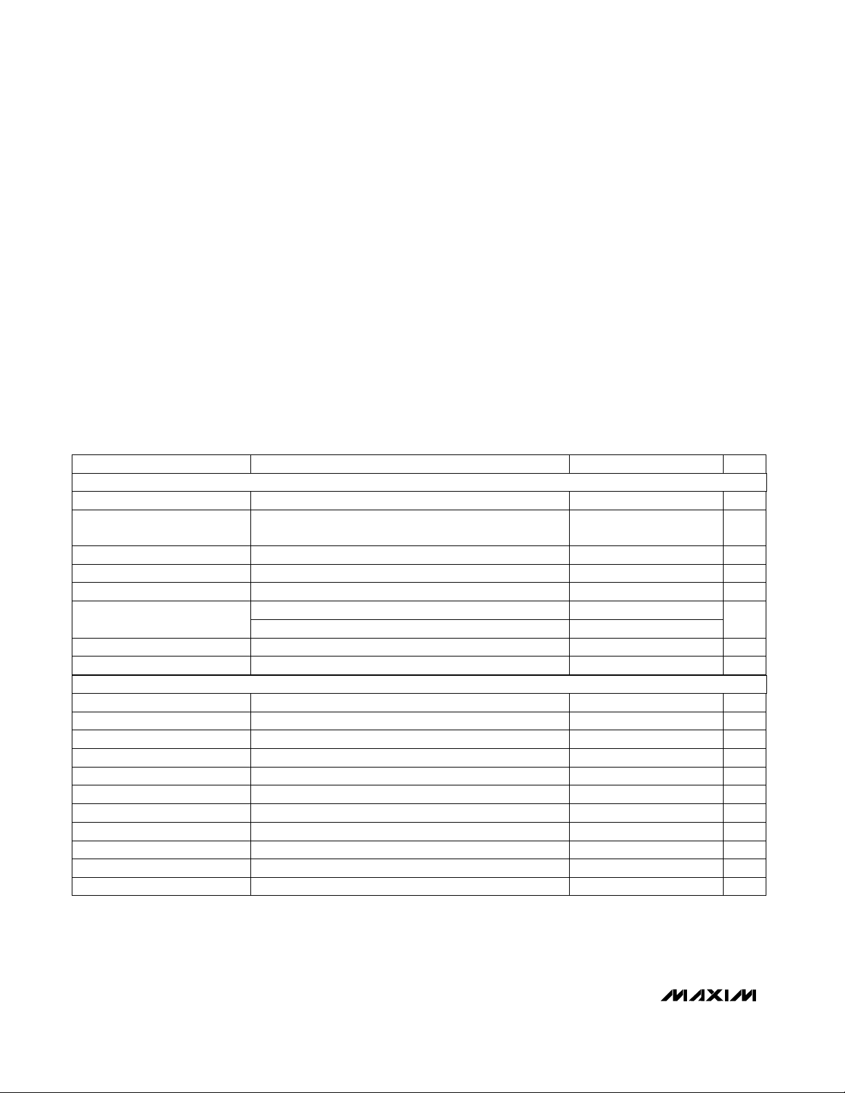
ELECTRICAL CHARACTERISTICS
(V+ = +15V, GND = PGND = 0V, IVL= I
STEP-DOWN CONTROLLER
Nominal Adjustable Output
Voltage Range
Current-Limit Voltage
INTERNAL REGULATOR AND REFERENCE
= 0A, TA= 0°C to +85°C, unless otherwise noted.)
REF
CONDITIONS
External resistor divider
CSH - CSL = 40mV, SKIP = VL
0mV < (CSH - CSL) < 80mV, SKIP = VL
6V < V+ < 30V
CSH - CSL, positive
CSH - CSL, negative
SHDN = 2V, 0mA <IVL< 25mA, 5.5V < V+ < 30V
Rising edge, hysteresis = 15mV
Rising edge, hysteresis = 25mV
No external load (Note 1) V2.463 2.505 2.537Reference Output Voltage
Falling edge V1.8 2.3Reference Fault Lockout Voltage
0µA < I
SHDN = 0V, CSL = 6V, V+ = 0V or 30V, VL = 0V
SHDN = 0V, V+ = 30V, CSL = 0V or 6V
FB = CSH = CSL = 6V, VL switched over to CSL µA15V+ Off-State Leakage Current
V+ = 4V, CSL = 0V (Note 2) mW6.6 10.5Dropout Power Consumption
CSH = CSL = 6V mW6.4 8.5Quiescent Power Consumption
REF
< 100µA mV20Reference Load Regulation
REF Short Circuit to GND...........................................Continuous
VL Output Current...............................................................50mA
Continuous Power Dissipation (T
SO (derate 8.70mW/°C above +70°C)........................696mW
Operating Temperature Range
MAX798ESE....................................................-40°C to +85°C
Storage Temperature Range.............................-65°C to +160°C
Lead Temperature (soldering, 10sec).............................+300°C
= +70°C)
A
80 100 120
-40 -100 -160
UNITSMIN TYP MAXPARAMETER
V4.5 30Input Supply Range
V1.6 6
V1.576 1.6 1.624Feedback Voltage
%±0.4Load Regulation
%/V0.04 0.05Line Regulation
mV
µA2.0 4.0 6.5SS Source Current
mA2.0SS Fault Sink Current
V4.75 5.25VL Output Voltage
V3.8 4.0VL Fault Lockout Voltage
V4.2 4.7VL/CSL Switchover Voltage
µA0.1 1CSL Shutdown Leakage Current
µA15V+ Shutdown Current
2 _______________________________________________________________________________________

High-Accuracy Step-Down Controller
with Synchronous Rectifier for CPU Power
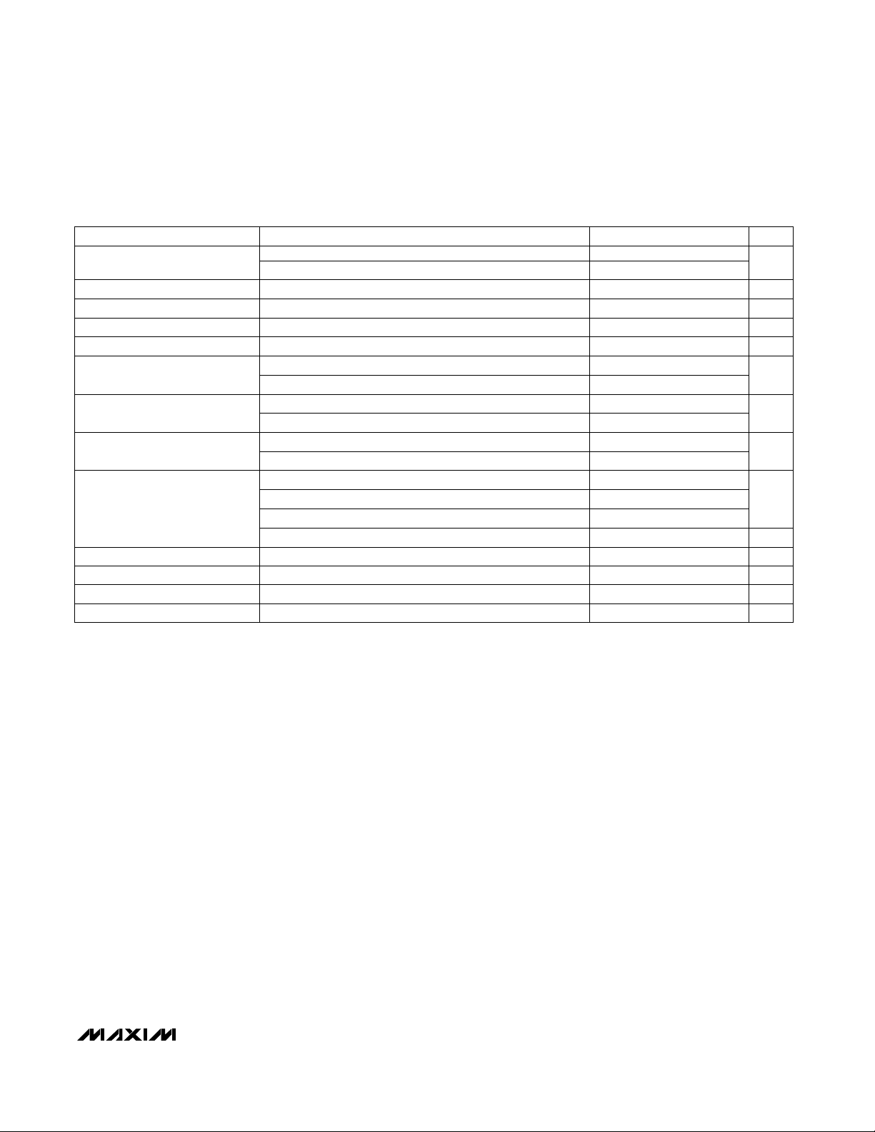
ELECTRICAL CHARACTERISTICS (continued)
(V+ = +15V, GND = PGND = 0V, IVL= I
Oscillator Frequency
Maximum Duty Cycle
Input High Voltage
Input Low Voltage
Input Current
= 0A, TA= 0°C to +85°C, unless otherwise noted.)
REF
CONDITIONS UNITSMIN TYP MAXPARAMETER
SYNC = REF
SYNC = 0V or 5V
Guaranteed by design
SYNC = REF
SYNC = 0V or 5V
SYNC
SHDN, SKIP
SYNC
SHDN, SKIP
SHDN, 0V or 30V
SYNC, SKIP
CSH, CSL, CSH = CSL = 4V, device not shut down
FB, FB = 1.6V ±100 nA
DL forced to 2V
DH forced to 2V, BST - LX = 4.5V A1DH Sink/Source Current
High or low
High or low, BST - LX = 4.5V
270 300 330
125 150 175
89 91
93 96
VL - 0.5
2.0
0.8
0.5
2
1
50
kHz
ns200SYNC High Pulse Width
ns200SYNC Low Pulse Width
ns200SYNC Rise/Fall Time
kHz195 340Oscillator Sync Range
%
V
V
µA
µA
A1DL Sink/Source Current
Ω7DL On-Resistance
Ω7DH On-Resistance
MAX798
_______________________________________________________________________________________ 3

High-Accuracy Step-Down Controller
with Synchronous Rectifier for CPU Power
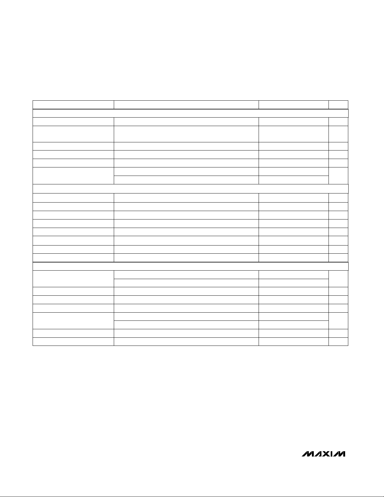
ELECTRICAL CHARACTERISTICS
(V+ = +15V, GND = PGND = 0V, IVL= I
STEP-DOWN CONTROLLER
Nominal Adjustable Output
MAX798
Voltage Range
Current-Limit Voltage
INTERNAL REGULATOR AND REFERENCE
OSCILLATOR AND INPUTS/OUTPUTS
Oscillator Frequency
Maximum Duty Cycle
= 0A, TA= -40°C to +85°C, unless otherwise noted.) (Note 3)
REF
CONDITIONS UNITSMIN TYP MAXPARAMETER
External resistor divider V1.6 6.0
CSH - CSL = 40mV, SKIP = VL
0mV < (CSH - CSL) < 80mV, SKIP = VL
6V < V+ < 30V %/ V0.04 0.06Line Regulation
CSH - CSL, positive
CSH - CSL, negative -40 -100 -160
SHDN = 2V, 0mA < IVL< 25mA, 5.5V < V+ < 30V
Rising edge, hysteresis = 15mV
Rising edge, hysteresis = 25mV
No external load (Note 1)
0µA < I
SHDN = 0V, V+ = 30V, CSL = 0V or 6V
FB = CSH = CSL = 6V, VL switched over to CSL
CSH = CSL = 6V
SYNC = REF
SYNC = 0V or 5V
SYNC = REF
SYNC = 0V or 5V
High or low
High or low, BST - LX = 4.5V
REF
< 100µA
70 130
4.15 4.75VL/CSL Switchover Voltage
250 300 350
110 150 190
250SYNC Low Pulse Width
88 91
92 96
V5.0 30Input Supply Range
V1.560 1.6 1.640Feedback Voltage
%±1Load Regulation
mV
V4.7 5.3VL Output Voltage
V3.75 4.05VL Fault Lockout Voltage
V
V2.438 2.505 2.562Reference Output Voltage
mV30Reference Load Regulation
µA110V+ Shutdown Current
µA110V+ Off-State Leakage Current
mW6.4 9.1Quiescent Power Consumption
kHz
ns250SYNC High Pulse Width
ns
kHz210 320Oscillator Sync Range
%
Ω7DL On-Resistance
Ω7DH On-Resistance
Note 1: Since the reference uses VL as its supply, V+ line-regulation error is insignificant.
Note 2: At very low input voltages, quiescent supply current can increase due to excess PNP base current in the VL linear
regulator. This occurs only if V+ falls below the preset VL regulation point (5V nominal). The typical maximum quiescent
current in dropout will not exceed 16mA.
Note 3: All -40°C to +85°C specifications above are guaranteed by design.
4 _______________________________________________________________________________________
 Loading...