

_______________General Description
The MAX797H high-performance, step-down DC-DC
converter provides main CPU power in battery-powered
systems. A 40V rating on the power stage’s input allows
operation with high-cell-count batteries and a wide
range of AC adaptors. This buck controller achieves
96% efficiency by using synchronous rectification and
Maxim’s proprietary Idle Mode™ control scheme to
extend battery life at full-load (up to 10A) and no-load
outputs. Excellent dynamic response corrects output transients caused by the latest dynamic-clock CPUs within five
300kHz clock cycles. Unique bootstrap circuitry drives
inexpensive N-channel MOSFETs, reducing system cost
and eliminating the crowbar switching currents found in
some PMOS/NMOS switch designs.
The MAX797H has a logic-controlled and synchronizable
fixed-frequency, pulse-width-modulating (PWM) operating
mode, which reduces noise and RF interference in sensitive mobile-communications and pen-entry applications.
The SKIP override input allows automatic switchover to
idle-mode operation (for high-efficiency pulse skipping) at
light loads, or forces fixed-frequency mode for lowest noise
at all loads. The MAX797H is pin compatible with the popular MAX797, but has a higher input voltage range.
The MAX797H comes in a 16-pin narrow SO package.
________________________Applications
Notebook and Subnotebook Computers
Industrial Controls
____________________________Features
♦ 96% Efficiency
♦ Up to 40V Power Input
♦ 2.5V to 6V Adjustable Output
♦ Preset 3.3V and 5V Outputs (at up to 10A)
♦ 5V Linear-Regulator Output
♦ Precision 2.505V Reference Output
♦ Automatic Bootstrap Circuit
♦ 150kHz/300kHz Fixed-Frequency PWM Operation
♦ Programmable Soft-Start
♦ 375µA Quiescent Current (VIN= 12V, V
OUT
= 5V)
♦ 1µA Shutdown Current
MAX797H
High-Voltage, Step-Down Controller with
Synchronous Rectifier for CPU Power
________________________________________________________________
Maxim Integrated Products
1
Idle Mode is a trademark of Maxim Integrated Products.
19-1239; Rev 0; 7/97
__________________Pin Configuration
16
15
14
13
12
11
10
9
1
2
3
4
5
6
7
8
DH
LX
BST
DLGND
REF
SKIP
SS
TOP VIEW
MAX797H
PGND
VL
V+
CSL
CSH
FB
SHDN
SYNC
SO
__________Typical Operating Circuit
MAX797H
SHDN
DH
+3.3V
OUTPUT
+4V TO +40V
POWER INPUT
BST
LX
DL
PGND
CSH
CSL
SS
REF
SYNC
GND
SKIP FB
V+
+4.5V TO +30V
SUPPLY
INPUT
VL
PIN-PACKAGETEMP. RANGEPART
†
16 Narrow SO-40°C to +85°CMAX797HESE
For free samples & the latest literature: http://www.maxim-ic.com, or phone 1-800-998-8800
For small orders, phone 408-737-7600 ext. 3468.
______________Ordering Information
†
U.S. and foreign patents pending.
MAX797H
High-Voltage, Step-Down Controller with
Synchronous Rectifier for CPU Power
2 _______________________________________________________________________________________
ABSOLUTE MAXIMUM RATINGS
ELECTRICAL CHARACTERISTICS
(V+ = 15V, GND = PGND = 0V, IVL= I
REF
= 0A, TA= 0°C to +85°C, SYNC = 0V, unless otherwise noted.)
Stresses beyond those listed under “Absolute Maximum Ratings” may cause permanent damage to the device. These are stress ratings only, and functional
operation of the device at these or any other conditions beyond those indicated in the operational sections of the specifications is not implied. Exposure to
absolute maximum rating conditions for extended periods may affect device reliability.
V+ to GND ................................................................-0.3V to 36V
GND to PGND........................................................................±2V
VL to GND...................................................................-0.3V to 7V
BST to GND ..............................................................-0.3V to 46V
DH to LX.....................................................-0.3V to (BST + 0.3V)
LX to BST....................................................................-7V to 0.3V
SHDN to GND...........................................................-0.3V to 36V
SYNC, SS, REF, FB, SKIP, DL to GND...........-0.3V to (VL + 0.3V)
CSH, CSL to GND.......................................................-0.3V to 7V
VL Short Circuit to GND..............................................Momentary
REF Short Circuit to GND...........................................Continuous
VL Output Current...............................................................50mA
Continuous Power Dissipation (T
A
= +70°C)
SO (derate 8.70mW/°C above +70°C)........................696mW
Operating Temperature Range
MAX797HESE.................................................-40°C to +85°C
Storage Temperature Range.............................-65°C to +160°C
Lead Temperature (soldering, 10sec).............................+300°C
Rising edge, hysteresis = 25mV
V+
Rising edge, hysteresis = 15mV
SHDN = 2V, 0mA < IVL< 25mA, 5.5V < V+ < 30V
CSH - CSL, negative
CSH - CSL, positive
FB = VL, 6V < power input < 40V (Note 4)
25mV < (CSH - CSL) < 80mV
0mV < (CSH - CSL) < 80mV, FB = VL,
6V < power input < 40V, includes line and load
regulation (Note 4)
External resistor divider
CSH - CSL = 0V
0mV < (CSH - CSL) < 80mV
CONDITIONS
V4.2 4.7VL/CSL Switchover Voltage
V3.8 4.1VL Fault Lockout Voltage
V4.7 5.3VL Output Voltage
mA2.0SS Fault Sink Current
µA2.5 4.0 6.5SS Source Current
40
V
4.5 30
Input Supply Range
-50 -100 -160
mV
80 100 120
Current-Limit Voltage
1.5
V4.85 5.10 5.255V Output Voltage (CSL)
VREF 6
Nominal Adjustable Output
Voltage Range
V2.43 2.505 2.57Feedback Voltage
%
2.5
Load Regulation
UNITSMIN TYP MAXPARAMETER
High-side MOSFET drain
0mV < (CSH - CSL) < 80mV, FB = 0V,
4.5V < power input < 40V, includes line and load
regulation (Note 4)
V3.20 3.35 3.463.3V Output Voltage (CSL)
FB = 0V, 4.5V < power input < 40V (Note 4)
%/V
0.04 0.06
Line Regulation
+3.3V AND +5V STEP-DOWN CONTROLLERS
FLYBACK/PWM CONTROLLERINTERNAL REGULATOR AND REFERENCE
0.04 0.06
MAX797H
High-Voltage, Step-Down Controller with
Synchronous Rectifier for CPU Power
_______________________________________________________________________________________ 3
ELECTRICAL CHARACTERISTICS (continued)
(V+ = 15V, GND = PGND = 0V, IVL= I
REF
= 0A, TA= 0°C to +85°C, SYNC = 0V, unless otherwise noted.)
SHDN, 0V or 30V
SHDN, SKIP
SYNC
SYNC = 0V or 5V
No external load (Note 1)
SYNC = REF
Guaranteed by design
CSH = CSL = 6V
V+ = 4V, CSL = 0V (Note 2)
SYNC = 0V or 5V
SHDN = 0V, V+ = 30V, CSL = 0V or 6V
Falling edge
0µA < I
REF
< 100µA
SYNC = REF
SHDN = 0V, CSL = 6V, V+ = 0V or 30V, VL = 0V
CONDITIONS
2.0
2.0
V
VL - 0.5
Input High Voltage
%
93 96
89 91
Maximum Duty Factor
kHz190 340Oscillator Sync Range
ns200SYNC Rise/Fall Time
ns200SYNC Low Pulse Width
ns200SYNC High Pulse Width
125 150 175
kHz
270 300 330
Oscillator Frequency
2.45 2.505 2.55 VReference Output Voltage
mW4.8 6.6Quiescent Power Consumption
mW4 8Dropout Power Consumption
1 5 µAV+ Shutdown Current
V1.8 2.3Reference Fault Lockout Voltage
mV50Reference Load Regulation
µA0.1 1CSL Shutdown Leakage Current
UNITSMIN TYP MAXPARAMETER
FB = CSH = CSL = 6V, VL switched over to CSL 1 5 µAV+ Off-State Leakage Current
DL forced to 2V
FB, FB = REF
CSH, CSL, CSH = CSL = 4V, device not shut down
SYNC, SKIP
A1DL Sink/Source Current
±100
50
1.0
SHDN, SKIP
SYNC
0.5
V
0.8
Input Low Voltage
DH forced to 2V, BST - LX = 4.5V A1DH Sink/Source Current
High or low, BST - LX = 4.5V
High or low
Ω7DH On-Resistance
Ω7DL On-Resistance
OSCILLATOR AND INPUTS/OUTPUTS
nA
Input Current
µA

%/V
MAX797H
High-Voltage, Step-Down Controller with
Synchronous Rectifier for CPU Power
4 _______________________________________________________________________________________
ELECTRICAL CHARACTERISTICS (continued)
(V+ = 15V, GND = PGND = 0V, IVL= I
REF
= 0A, TA= -40 to +85°C, SYNC = 0V, unless otherwise noted.) (Note 3)
Note 1: Since the reference uses VL as its supply, V+ line-regulation error is insignificant.
Note 2: At very low input voltages, quiescent supply current can increase due to excess PNP base current in the VL linear
regulator. This occurs only if V+ falls below the preset VL regulation point (5V nominal).
Note 3: All -40°C to +85°C specifications are guaranteed by design.
Note 4: The power input is the high-side MOSFET drain.
External resistor divider
0mV < (CSH - CSL) < 80mV, FB = 0V,
4.5V < power input < 40V, includes line and load
regulation (Note 4)
V+
0mV < (CSH - CSL) < 80mV, FB = VL,
6V < power input < 40V, includes line and load
regulation (Note 4)
CONDITIONS
VREF 6.0
Nominal Adjustable Output
Voltage Range
V3.10 3.35 3.563.3V Output Voltage (CSL)
5.0 30
V4.70 5.10 5.405V Output Voltage (CSL)
UNITSMIN TYP MAXPARAMETER
CSH - CSL, negative
CSH - CSL = 0V
FB = VL, 6V < power input < 40V (Note 4)
CSH - CSL, positive
-40 -100 -160
Current-Limit Voltage
V2.40 2.60Feedback Voltage
0.04 0.06
mV
70 130
FB = CSH = CSL = 6V, VL switched over to CSL
SHDN = 0V, V+ = 30V, CSL = 0V or 6V
Rising edge, hysteresis = 25mV
No external load (Note 1)
0µA < I
REF
< 100µA
µA1 10V+ Off-State Leakage Current
µA1 10V+ Shutdown Current
V
Rising edge, hysteresis = 15mV
SHDN = 2V, 0mA < IVL< 25mA, 5.5V < V+ < 30V
4.2 4.7VL/CSL Switchover Voltage
V2.43 2.505 2.57Reference Output Voltage
mV50Reference Load Regulation
V3.75 4.15VL Fault Lockout Voltage
V4.7 5.3VL Output Voltage
SYNC = REF
SYNC = 0V or 5V
89 91
kHz210 320Oscillator Sync Range
kHz
SYNC = REF
120 150 180
Oscillator Frequency
ns250SYNC High Pulse Width
ns
CSH = CSL = 6V
250SYNC Low Pulse Width
250 300 350
mW4.8 8.4Quiescent Power Consumption
High or low, BST - LX = 4.5V
High or low
SYNC = 0V or 5V
Ω7DH On-Resistance
Ω7DL On-Resistance
%
93 96
Maximum Duty Factor
High-side MOSFET drain
V
40
Input Supply Range
FB = 0V, 4.5V < power input < 40V (Note 4)
%/V
0.04 0.06
Line Regulation
+3.3V and +5V STEP-DOWN CONTROLLERS
FLYBACK/PWM CONTROLLERINTERNAL REGULATOR AND REFERENCE
OSCILLATOR AND INPUTS/OUTPUTS

MAX797H
High-Voltage, Step-Down Controller with
Synchronous Rectifier for CPU Power
_______________________________________________________________________________________ 5
______________________________________________________________Pin Description
Dual Mode is a trademark of Maxim Integrated Products.
Rail-to-Rail is a registered trademark of Nippon Motorola Ltd.
SKIP
Disables pulse-skipping mode when high. Connect SKIP to GND for normal use. Do not leave unconnected.
With SKIP grounded, the device
automatically
changes from pulse-skipping operation to full PWM operation
when the load current exceeds approximately 30% of maximum.
16 DH
High-Side Gate-Drive Output. DH normally drives the main buck switch. It is a floating driver output that
swings from LX to BST, riding on the LX switching-node voltage.
15 LX Switching Node (inductor) Connection. LX can swing 2V below ground without hazard.
14 BST Boost Capacitor Connection for High-Side Gate Drive (0.1µF)
13 DL Low-Side Gate-Drive Output. DL normally drives the synchronous-rectifier MOSFET. Swings 0V to VL.
NAME FUNCTION
1 SS Soft-Start Timing Capacitor Connection. Ramp time to full current limit is approximately 1ms/nF.
2
PIN
3 REF Reference Voltage Output. Bypass REF to GND with 0.33µF minimum.
7 FB
Feedback Input. Regulates at FB = REF (approximately 2.505V) in adjustable mode. FB is a Dual Mode
TM
input that also selects the fixed-output voltage settings as follows:
• Connect to GND for 3.3V operation.
• Connect to VL for 5V operation.
• Connect to a resistor divider for adjustable mode. FB can be driven with 5V Rail-to-Rail®logic to change
the output voltage under system control.
6
SHDN
Shutdown Control Input, Active Low. Logic threshold is set at approximately 1V (VTHof an internal N-channel
MOSFET). Tie SHDN to V+ for automatic start-up.
5 SYNC
Oscillator Synchronization and Frequency Select. Tie SYNC to GND or VL for 150kHz operation; tie to REF for
300kHz operation. A high-to-low transition begins a new cycle. Drive SYNC with 0V to 5V logic levels (see
Electrical Characteristics
for VIHand VILspecifications). SYNC capture range is guaranteed to be 190kHz to
340kHz.
4 GND Low-noise Analog Ground and Feedback Reference Point
12 PGND Power Ground
11 VL
5V Internal Linear-Regulator Output. VL is also the supply-voltage rail for the chip. It is switched to the output
voltage via CSL (V
CSL
> 4.5V) for automatic bootstrapping. Bypass to GND with 4.7µF. VL can supply up to
5mA for external loads.
10 V+
Battery Voltage Input (4.5V to 30V). Bypass V+ to PGND close to the IC with a 0.1µF capacitor. Connects to a
linear regulator that powers VL.
9 CSL Current-Sense Input, Low Side. CSL also serves as the feedback input in fixed-output modes.
8 CSH Current-Sense Input, High Side. Current-limit level is 100mV referred to CSL.

MAX797H
_______________Detailed Description
The MAX797H is functionally identical to the MAX797.
The only difference between the two devices is in the
BST pin’s absolute maximum rating. The MAX797H’s
rating is 46V; the MAX797’s rating is 36V. The higher
rating allows the MAX797H to use a power input up to
40V, provided that the V+ pin is powered by a separate
supply between 4.5V and 30V.
Circuit design and component selection for the
MAX797H are identical to those for the MAX797; therefore, such information is not included in this data sheet.
Refer to the MAX796/MAX797/MAX799 data sheet for
design formulas and applications information. The
Applications Information
section in this data sheet contains suggestions for providing the 30V maximum V+
supply input for the MAX797H when power input
exceeds 30V.
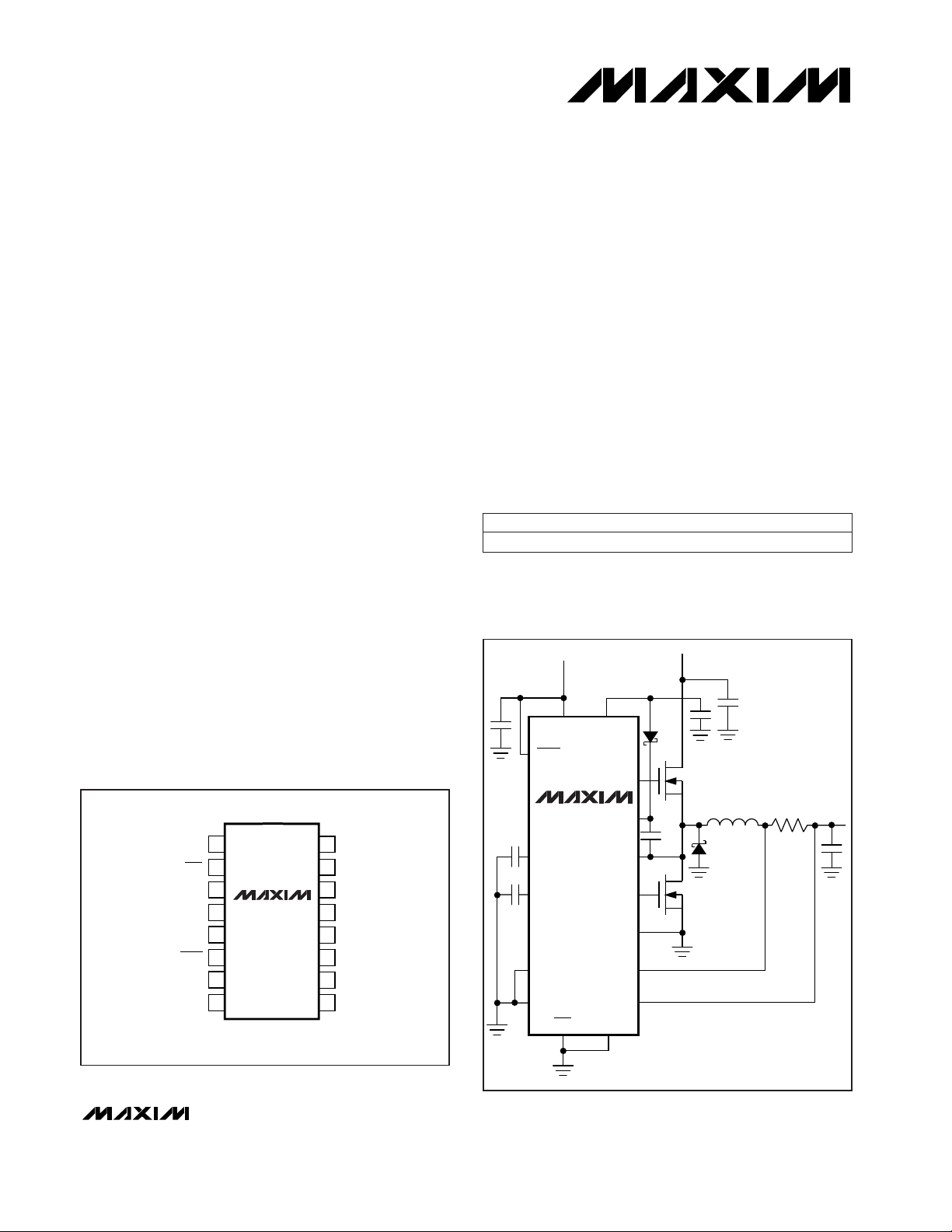
__________Applications Information
Powering the V+ Pin
V+ can be supplied directly if a system supply between
4.5V and 30V is available (see the
Typical Operating
Circuit
). Most of the MAX797H’s internal blocks are supplied by VL, which uses V+ as its input. While the current into V+ is minimal, it depends heavily on the type of
external MOSFET used and the switching frequency:
I
GATE
= Qgx f
SW
where Qgis the sum of the high- and low-side
MOSFET’s total gate charges, and fSWis the switching
frequency. Furthermore, if the circuit output voltage on
CSL exceeds the VL/CSL switchover voltage, the
MAX797H bootstraps itself (it connects VL to CSL and
turns off the linear regulator, supplying the IC from the
circuit output), and V+ current is reduced to about 1µA.
If a 5V regulated supply is available, V+ and VL can be
connected and fed from that supply (Figure 1). In this
mode, the VL regulator is bypassed. Do not use this
approach if the output voltage on CSL can exceed the
VL/CSL switchover voltage.
If a 5V regulated supply is not available, a linear regulator with a sufficient input voltage range can provide it
(Figure 2). This approach allows for a very wide input
voltage range, which is useful if the circuit must run from
several different power sources. The drawback of the
linear regulator is the high quiescent current that these
devices typically require, in addition to the current used
by the feedback divider resistors (R1 and R2).
For most applications, a better choice than Figure 2’s
circuit takes advantage of the MAX797H’s internal linear regulator. There is no need to provide a regulated
supply to V+, provided it is within the +4.5V to +30V V+
input voltage range. In Figure 3, Q1 is used to drop a
40V (max) input to 30V by dividing it by approximately
4/3. This approach results in a somewhat higher minimum input voltage than that of Figure 2’s circuit, but a
much lower quiescent current than that of a linear regulator. If quiescent current must be minimized, an
N-channel MOSFET can be substituted for Q1, and the
divider-resistor values can be increased.
Powering V+ with a zener diode can be done in many
different ways. The simplest is to use a standard shunt
regulator to provide a regulated voltage in the 4.5V to
30V range (Figure 4). Resistor R1 must be chosen to
allow the maximum required V+ current to be obtained
from the minimum power input voltage. If the power
input voltage varies appreciably, the result is higherthan-necessary input current from the highest power
input voltage. An approach that reduces quiescent
current is to use a zener diode as a dropping diode to
keep V+ under 30V (Figure 5). This results in a severely
restricted minimum range for the power input voltage,
which is not a problem for most high-voltage applications. RL must be added to draw current and to ensure
that there is sufficient forward drop across the zener
diode if the MAX797H can be shut down or bootstrap
off its output voltage.
Duty-Factor Limitations for
Low V
OUT/VIN
Ratios
The MAX797H’s output voltage is adjustable down to
2.5V (min). However, the combination of high input and
low output voltages may not be possible at high switching frequencies without introducing some amount of
frequency instability. The minimum duty factor is determined by delays through the error comparator, internal
logic, gate drivers, and external MOSFETs. The delay is
typically 425ns. With a switching period of 3.33µs
(300kHz), the minimum duty factor is 0.425µs / 3.33µs
= 0.13. If V
OUT
/ VINis less than this value, the IC will
properly regulate the output voltage, but may extend
the period and switch at 150kHz instead of 300kHz. It
may also alternate between these two frequencies. For
example, if VINis 40V, the lowest V
OUT
that does not
require less than the minimum duty factor is 40V x 0.13
= 5.2V. Below this output voltage, select the 150kHz
switching frequency (connect SYNC to VL or GND).
High-Voltage, Step-Down Controller with
Synchronous Rectifier for CPU Power
6 _______________________________________________________________________________________

MAX797H
High-Voltage, Step-Down Controller with
Synchronous Rectifier for CPU Power
_______________________________________________________________________________________ 7
Figure 1. Powering V+ and VL from a Regulated +5V supply
MAX797H
SHDN
DH
+3.3V
OUTPUT
+4V TO +40V
POWER INPUT
BST
LX
DL
PGND
CSH
CSL
SS
REF
SYNC
GND
SKIP FB
V+
+5V
REGULATED
SUPPLY
VL
Similarly, at 150kHz, the minimum duty factor is
0.425µs / 6.67µs = 0.064. This means that duty factor is
not an issue except at the maximum input voltage and
minimum output voltage. For example, if VINis 40V,
the lowest V
OUT
that does not require less than the
minimum duty factor is 40V x 0.064 = 2.56V. If V
OUT
/
VINis less than this value, the IC will properly regulate
the output voltage, but may extend the period and
switch at 75kHz instead of 150kHz. It may also alternate between these two frequencies.

Maxim cannot assume responsibility for use of any circuitry other than circuitry entirely embodied in a Maxim product. No circuit patent licenses are
implied. Maxim reserves the right to change the circuitry and specifications without notice at any time.
8
___________________Maxim Integrated Products, 120 San Gabriel Drive, Sunnyvale, CA 94086 (408) 737-7600
© 1997 Maxim Integrated Products Printed USA is a registered trademark of Maxim Integrated Products.
MAX797H
High-Voltage, Step-Down Controller with
Synchronous Rectifier for CPU Power
___________________Chip Information
TRANSISTOR COUNT: 913
MAX797H
SHDN
DH
+7V TO +40V
INPUT
V+ VL
OUT
ADJ
IN
R1
R2
Figure 2. Powering V+ and VL with a +5V Linear Regulator Figure 3. Dividing the Power Input to Supply V+
Figure 4. Powering V+ with a Zener Shunt Regulator
Figure 5. Powering V+ with a Zener Dropping Diode
Q1
V+ VL
SHDN
+8V TO +40V
POWER INPUT
100k
300k
MAX797H
DH
UP TO +40V
POWER INPUT
12V
R1
R1
V+ VL
SHDN
MAX797H
DH
V+ VL
SHDN
MAX797H
DH
+20V TO +40V
POWER INPUT
 Loading...