Maxim MAX793SCPE, MAX793SCSE, MAX793RCPE, MAX793RCSE, MAX793REPE Datasheet
...
For free samples & the latest literature: http://www.maxim-ic.com, or phone 1-800-998-8800
_______________General Description
The MAX793/MAX794/MAX795 microprocessor (µP)
supervisory circuits monitor and control the activities of
+3.0V/+3.3V µPs by providing backup-battery switchover,
among other features such as low-line indication, µP
reset, write protection for CMOS RAM, and a watchdog
(see the
Selector Guide
below). The backup-battery voltage can exceed VCC, permitting the use of 3.6V lithium
batteries in systems using 3.0V to 3.3V for VCC.
The MAX793/MAX795 offer a choice of reset threshold
voltage range (denoted by suffix letter): 3.00V to 3.15V
(T), 2.85V to 3.00V (S), and 2.55V to 2.70V (R). The
MAX794’s reset threshold is set externally with a resistor
divider. The MAX793/MAX794 are available in 16-pin
DIP and narrow SO packages, and the MAX795 comes
in 8-pin DIP and SO packages. For similar devices
designed for 5V systems, see the
µP Supervisory
Circuits
table at the back of this data sheet.
________________________Applications
Battery-Powered Computers and Controllers
Embedded Controllers
Intelligent Controllers
Critical µP Power Monitoring
Portable Equipment
____________________________Features
MAX793/MAX794/MAX795
♦ Precision Supply-Voltage Monitor:
Fixed Reset Trip Voltage (MAX793/MAX795)
Adjustable Reset Trip Voltage (MAX794)
♦ Guaranteed Reset Assertion to VCC= 1V
♦ Backup-Battery Power Switching—Battery
Voltage Can Exceed V
CC
♦ On-Board Gating of Chip-Enable Signals—7ns
Max Propagation Delay
MAX793/MAX794 Only
♦ Battery Freshness Seal
♦ Battery OK Output (MAX793)
♦ Uncommitted Voltage Monitor for Power-Fail or
Low-Battery Warning
♦ Independent Watchdog Timer (1.6sec timeout)
♦ Manual Reset Input
______________Ordering Information
Ordering Information continued on last page.
* The MAX793/MAX795 offer a choice of reset threshold voltage.
Select the letter corresponding to the desired reset threshold
voltage range (T = 3.00V to 3.15V, S = 2.85V to 3.00V, R = 2.55V
to 2.70V) and insert it into the blank to complete the part number.
The MAX794’s reset threshold is adjustable.
MAX793/MAX794/MAX795
3.0V/3.3V Adjustable Microprocessor
Supervisory Circuits
________________________________________________________________
Maxim Integrated Products
1
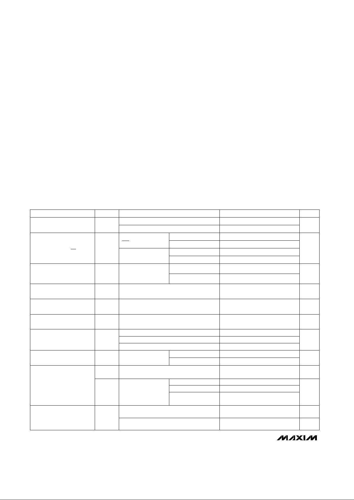
MAX793
RESET
LOWLINE
WDI
CE IN
CE OUT
3.0V OR 3.3V
+5V
BATT
A0-A15
MR
+5V SUPPLY
FAILURE
BATT ON
PFI
WDO
OUT
CMOS
RAM
ADDRESS
DECODER
0.1µF
PMOS
0.1µF
V
CC
PFO
GND
I/O
µP
NMI
RESET
V
CC
V
CC
0.1µF
3.6V
BATT OK
(OPTIONAL)
Si9433DY
SILICONIX
19-0366; Rev 1; 1/96
PART*
MAX793_CPE
MAX793_CSE
MAX793_EPE -40°C to +85°C
0°C to +70°C
0°C to +70°C
TEMP. RANGE PIN-PACKAGE
16 Plastic DIP
16 Narrow SO
16 Plastic DIP
MAX793_ESE -40°C to +85°C 16 Narrow SO
FEATURE
Active-Low Reset
Active-High Reset
Programmable Reset
Threshold
Low-Line Early Warning
Output
MAX793
✔
✔
✔
MAX794
✔
✔
✔
✔
MAX795
✔
Backup-Battery
Switchover
External Switch Driver
Power-Fail Comparator
✔
✔
✔
✔
✔
✔
Battery OK Output
✔
✔
✔
_____________________Selector Guide
__________Typical Operating Circuit
Watchdog Input
Battery Freshness Seal
✔
✔
✔
✔
Manual Reset Input
✔
✔
✔
Chip-Enable Gating
✔ ✔
Pins-Package 16-DIP/SO 16-DIP/SO 8-DIP/SO
Pin Configurations appear at end of data sheet.
µA
MAX793/MAX794/MAX795
3.0V/3.3V Adjustable Microprocessor
Supervisory Circuits
2 _______________________________________________________________________________________
ABSOLUTE MAXIMUM RATINGS
ELECTRICAL CHARACTERISTICS
(VCC= 3.17V to 5.5V for the MAX793T/MAX795T, VCC= 3.02V to 5.5V for the MAX793S/MAX795S, VCC= 2.72V to 5.5V for the
MAX793R/MAX794/MAX795R, V
BATT
= 3.6V, TA= T
MIN
to T
MAX
, unless otherwise noted. Typical values are at TA= +25°C.)
Stresses beyond those listed under “Absolute Maximum Ratings” may cause permanent damage to the device. These are stress ratings only, and functional
operation of the device at these or any other conditions beyond those indicated in the operational sections of the specifications is not implied. Exposure to
absolute maximum rating conditions for extended periods may affect device reliability.
Terminal Voltage (with respect to GND)
V
CC
........................................................................-0.3V to 6.0V
V
BATT
.....................................................................-0.3V to 6.0V
All Other Inputs ..................-0.3V to the higher of V
CC
or V
BATT
Continuous Input Current
V
CC
.................................................................................200mA
V
BATT
................................................................................50mA
GND..................................................................................20mA
Output Current
V
OUT
................................................................................200mA
All Other Outputs ..............................................................20mA
Continuous Power Dissipation (T
A
= +70°C)
8-Pin Plastic DIP (derate 9.09mW/°C above +70°C) .....727mW
8-Pin SO (derate 5.88mW/°C above +70°C)..................471mW
16-Pin Plastic DIP (derate 10.53mW/°C above +70°C) .842mW
16-Pin Narrow SO (derate 9.52mW/°C above +70°C)...696mW
Operating Temperature Ranges
MAX793_C_ _/MAX794C_ _/MAX795_C_ _......... 0°C to +70°C
MAX793_E_ _/MAX794E_ _/MAX795_E_ _........-40°C to +85°C
Storage Temperature Range.............................-65°C to +160°C
Lead Temperature (soldering, 10sec).............................+300°C
MAX79_E
MAX79_C
V
BATT
> V
CC
(Note 6)
I
OUT
= 250µA (Note 4)
I
OUT
= 30mA (Note 4)
VSW> VCC> 1.75V (Note 5)
I
OUT
= 75mA
V
BATT
= 2.3V
CONDITIONS
Battery Switch Threshold
(VCCfalling)
V
2.30 2.41 2.52
V
SW
2.55 2.68 2.80
2.69 2.82 2.95
mV20 65
VCC-
V
BATT
V
V
BATT
- 0.14
V
OUT
OUT Output Voltage in
Battery-Backup Mode
V
BATT
- 0.1 V
BATT
- 0.034
V
1.1 5.5
1.0 5.5
Operating Voltage Range,
V
CC
, V
BATT
(Note 1)
V
VCC- 0.001 VCC- 0.5mV
V
OUT
OUT Output Voltage in
Normal Mode
VCC- 0.12 VCC- 0.050
VCC- 0.3 VCC- 0.125
µA0.5
Battery Leakage Current
(Note 3)
µA1
BATT Supply Current
(excluding I
OUT
) (Note 2)
UNITSMIN TYP MAXSYMBOLPARAMETER
VCC= 0V, V
OUT
= 0V µA1
BATT Leakage Current,
Freshness Seal Enabled
I
OUT
= 250µA
I
OUT
= 1mA
MAX793T/MAX795T
MAX793S/MAX795S
This value is identical to the reset threshold,
VCCrising for V
BATT
> V
RST
VCC-
V
BATT
MAX793R/MAX795R/
MAX794
V
BATT
< V
RST
mV25 65
Battery Switch Threshold
(VCCrising) (Note 7)
MAX793/MAX794,
MR = V
CC
µA
62 80
I
SUPPLY
46 60
VCCSupply Current
(excluding I
OUT
, I
CE OUT
)
VCC= 2.1V,
V
BATT
= 2.3V
µA
32 45
I
SUPPLY
VCCSupply Current in
Battery-Backup Mode
(excluding I
OUT
)
VCC< 3.6V
VCC< 5.5V
MAX793/MAX794
MAX795 24 35
MAX795
49 70
35 50VCC< 3.6V
VCC< 5.5V
MAX793/MAX794/MAX795
3.0V/3.3V Adjustable Microprocessor
Supervisory Circuits
_______________________________________________________________________________________ 3
ELECTRICAL CHARACTERISTICS (continued)
(VCC= 3.17V to 5.5V for the MAX793T/MAX795T, VCC= 3.02V to 5.5V for the MAX793S/MAX795S, VCC= 2.72V to 5.5V for the
MAX793R/MAX794/MAX795R, V
BATT
= 3.6V, TA= T
MIN
to T
MAX
, unless otherwise noted. Typical values are at TA= +25°C.)
CONDITIONS
2.85 2.925 3.00
3.00 3.075 3.15
UNITSMIN TYP MAXSYMBOLPARAMETER
VCCFalling
3.00 3.085 3.17
2.55 2.625 2.70
V
RST
V
V
RST IN
V
VCCFalling
VCCRising
RESET IN Threshold
(MAX794 only)
1.212 1.240 1.262
Reset Threshold (Note 8)
2.55 2.635 2.72
2.85 2.935 3.02
V
LR
mV
MAX793
LOWLINE-to-Reset
Threshold, (V
LOWLINE
-
V
RST
), VCCFalling
VCC< 3.6V
51525
30 45 60
mV
MAX793S/MAX795S
MAX793T/MAX795T
MAX794
MAX793
3.08
Low-Line Comparator
Hysteresis
3.23
mV
10
10
mst
RP
140 200 280Reset Timeout Period
V
MAX793R/MAX795R 2.78
nA
V
PFI
rising
V
PFI
falling
PFI Input Current
MAX794
V
-25 2 25
V
TH
1.212 1.250 1.287
PFI Input Threshold
1.212 1.240 1.262
V
LL
1.317
LOWLINE Threshold,
VCCRising
VV
BOK
2.00 2.25 2.50
BATT OK Threshold
(MAX793)
V
OH
VI
SOURCE
= 300µA, VCC= V
RST
max
BATT OK, BATT ON, WDO,
LOWLINE Output Voltage
High
I
SOURCE
=300µA, VCC= V
RST
min
0.8V
CC
0.86V
CC
VV
OH
0.8V
CC
0.86V
CC
RESET Output Voltage High
mV10 20PFI Hysteresis, PFI Rising
MAX793T/MAX795T
MAX793S/MAX795S
MAX793R/MAX795R
MAX793T/MAX795T
MAX793S/MAX795S
MAX793R/MAX795R
nA
RESET IN Leakage Current
(MAX794 only)
-25 2 25
MAX794
V
OH
VI
SOURCE
= 65µA, VCC= V
RST
maxPFO Output Voltage High 0.8V
CC
V
OH
VI
SOURCE
= 100µA, VCC= 2.3V, V
BATT
= 3V
BATT ON Output
Voltage High
0.8V
BATT
I
LEAK
µAVCC= V
RST
max
RESET Output Leakage
Current (Note 9)
-1 -1
I
SC
µAVCC= 3.3V, V
PFO
= 0V
PFO Output Short to GND
Current
180 500
V
OL
V
I
SINK
= 1.2mA; RESET, LOWLINE tested
with VCC= V
RST
min; RESET, BATTOK,
WDO tested with VCC= V
RST
max
PFO, RESET, RESET, WDO,
LOWLINE Output Voltage
Low
0.08 0.2V
CC
INPUT AND OUTPUT LEVELS
VCCRising 1.212 1.250 1.282
MAX793/MAX794/MAX795
3.0V/3.3V Adjustable Microprocessor
Supervisory Circuits
4 _______________________________________________________________________________________
CONDITIONS
V
OL
V
V
OL
VI
SINK
= 3.2mA, VCC= V
RST
max
MAX79_E, V
BATT
= VCC= 1.2V, I
SINK
= 200µA
BATT ON Output
Voltage Low
MAX79_C, V
BATT
= VCC= 1.0V, I
SINK
= 40µA
0.2V
CC
RESET Output Voltage Low
UNITSMIN TYP MAXSYMBOLPARAMETER
V
IL
V
t
MR
nsMAX793/MAX794 only
V
RST
max < VCC< 5.5V
MR Pulse Width 100 50
All Inputs Including PFO
(Note 10)
0.3V
CC
V
IH
0.7V
CC
0.17 0.3
0.13 0.3
ELECTRICAL CHARACTERISTICS (continued)
(VCC= 3.17V to 5.5V for the MAX793T/MAX795T, VCC= 3.02V to 5.5V for the MAX793S/MAX795S, VCC= 2.72V to 5.5V for the
MAX793R/MAX794/MAX795R, V
BATT
= 3.6V, TA= T
MIN
to T
MAX
, unless otherwise noted. Typical values are at TA= +25°C.)
t
MD
ns
MAX793/MAX794 only, MR = 0V
MAX793/MAX794 only
µA
MR-to-Reset Delay
25 70 250MR Pull-Up Current
75 250
Ω
nsVCC= V
RST
max, Figure 9
Enable mode, VCC= V
RST
max
CE IN-to-CE OUT
Propagation Delay
Disable mode
27
CE IN-to-CE OUT
Resistance
V
OH
V
OL
V
VCC= V
RST
max, I
OUT
= 1.6mA,
V
CE IN
= 0V
VCC= V
RST
max, I
OUT
= -1mA,
V
CE IN
= V
CC
CE OUT Drive from CE IN
0.2V
CC
0.8V
CC
nA
46
I
LEAK
±10CE IN Leakage Current
Note 1: VCCsupply current, logic input leakage, watchdog functionality (MAX793/MAX794), MR functionality (MAX793/MAX794),
PFI functionality (MAX793/MAX794), state of RESET
and RESET (MAX793/MAX794) tested at V
BATT
= 3.6V and VCC= 5.5V.
The state of RESET
is tested at VCC= VCCmin.
Note 2: Tested at V
BATT
= 3.6V, VCC= 3.5V and 0V. The battery current will rise to 10µA over a narrow transition window around
V
CC
= 1.9V.
Note 3: Leakage current into the battery is tested under the worst-case conditions at V
CC
= 5.5V, V
BATT
= 1.8V and VCC= 1.5V,
V
BATT
= 1.0V.
Note 4: Guaranteed by design.
Note 5: When V
SW
> VCC> V
BATT
, OUT remains connected to VCCuntil VCCdrops below V
BATT
. The VCC-to-V
BATT
comparator
has a small 15mV typical hysteresis to prevent oscillation. For V
CC
< 1.75V (typical), OUT switches to BATT regardless of
V
BATT
.
Note 6: When V
BATT
> VCC> VSW, OUT remains connected to VCCuntil VCCdrops below the battery switch threshold (VSW).
Note 7: OUT switches from BATT to V
CC
when VCCrises above the reset threshold, if V
BATT
> V
RST
. In this case, switchover back
to V
CC
occurs at the exact voltage that causes reset to be asserted, however switchover occurs 200ms prior to reset. If
V
BATT
< V
RST
, OUT switches from BATT to VCCwhen VCCexceeds V
BATT
.
Note 8: The reset threshold tolerance is wider for V
CC
rising than for VCCfalling to accommodate the 10mV typical hysteresis,
which prevents internal oscillation.
Note 9: The leakage current into or out of the RESET
pin is tested with RESET not asserted (RESET output high impedance).
Note 10: PFO
is normally an output, but is used as an input when activating the battery freshness seal.
µs10Reset to CE OUT High Delay
t
WD
sec
0V < VCC< 5.5V
Watchdog Timeout Period
IOH= 500µA, VCC< 2.3V
µA
1.00 1.60 2.25
-1 0.01 1WDI Input Current
VV
OH
0.8V
BATT
CE OUT Output Voltage
High (reset active)
nsWDI Pulse Width 1.00
MANUAL RESET INPUT
CHIP-ENABLE GATING
WATCHDOG (MAX793/MAX794 only)
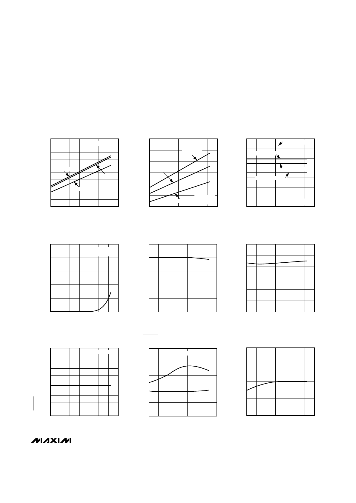
MAX793/MAX794/MAX795
3.0V/3.3V/Adjustable Microprocessor
Supervisory Circuits
_______________________________________________________________________________________
5
3.0
2.8
2.6
2.4
2.2
2.0
1.8
1.6
1.4
1.2
1.0
-40 100
VCC-TO-OUT ON-RESISTANCE
vs. TEMPERATURE
MAX793 TOC1
TEMPERATURE (°C)
V
CC
-TO-OUT ON-RESISTANCE (Ω)
20-20 0 8040 60
I
OUT
= 30mA
VCC = 3.0V
VCC = 3.3V
VCC = 5V
160
140
120
100
80
60
40
-40 100
BATT-TO-OUT ON-RESISTANCE
vs. TEMPERATURE
MAX793 TOC2
TEMPERATURE (°C)
BATT-TO-OUT ON-RESISTANCE (Ω)
20-20 0 8040 60
V
BATT
= 3.6V
V
BATT
= 3.0V
V
BATT
= 5V
I
OUT
= 250µA
V
CC
= 0V
70
60
50
40
30
20
10
0
-40 100
VCC SUPPLY CURRENT vs. TEMPERATURE
(NORMAL OPERATING MODE)
MAX793 TOC3
TEMPERATURE (°C)
V
CC
SUPPLY CURRENT (µA)
20-20 0 8040 60
MAX793/4, VCC = 3.3V
MAX795, VCC = 3.3V
MAX793/4, VCC = 5V
V
BATT
= VCC = V
OUT
MAX795, VCC = 5V
0.10
0.08
0.06
0.04
0.02
0
-40 100
BATTERY SUPPLY CURRENT vs.
TEMPERATURE (BATTERY-BACKUP MODE)
MAX793 TOC4
TEMPERATURE (°C)
SUPPLY CURRENT (µA)
20-20 0 8040 60
VCC = 0V
V
BATT
= 3.6V
100
90
80
70
60
50
40
30
20
10
0
-40 100
MAX793
LOWLINE-TO-RESET THRESHOLD
vs. TEMPERATURE
MAX793 TOC7
TEMPERATURE (°C)
LOWLINE-TO-RESET THRESHOLD (mV)
20-20 0 8040 60
VCC FALLING
250
200
150
100
50
0
-40 100
RESET TIMEOUT PERIOD
vs. TEMPERATURE
MAX793 TOC5
TEMPERATURE (°C)
RESET TIMEOUT PERIOD (ms)
20-20 0 8040 60
VCC RISING FROM
OV TO V
RST
MAX
30
25
20
15
10
5
0
-40 100
RESET COMPARATOR PROPAGATION DELAY
vs. TEMPERATURE (V
CC
FALLING)
MAX793 TOC6
TEMPERATURE (°C)
PROPAGATION DELAY (µs)
20-20 0 8040 60
10
8
6
4
2
0
-40 100
MAX793/MAX794
LOWLINE COMPARATOR PROPAGATION DELAY
vs. TEMPERATURE
MAX793 TOC8
TEMPERATURE (°C)
PROPAGATION DELAY (µs)
20-20 0 8040 60
40mV OVERDRIVE
VCC RISING
VCC FALLING
1.250
1.245
1.240
1.235
1.230
-40 100
MAX793/MAX794
PFI THRESHOLD vs. TEMPERATURE
MAX793 TOC9
TEMPERATURE (°C)
PFI THRESHOLD (V)
20-20 0 8040 60
__________________________________________Typical Operating Characteristics
(TA = +25°C, unless otherwise noted.)
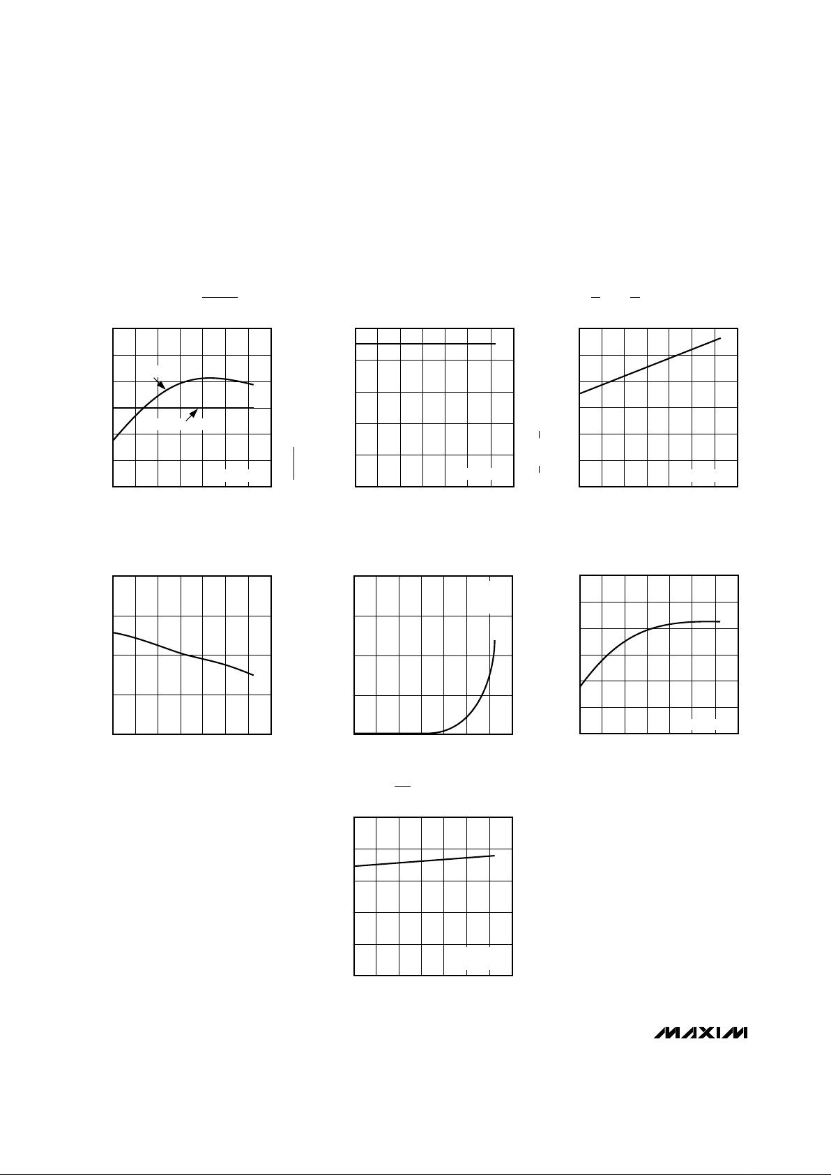
MAX793/MAX794/MAX795
3.0V/3.3V Adjustable Microprocessor
Supervisory Circuits
6 _______________________________________________________________________________________
____________________________Typical Operating Characteristics (continued)
(TA = +25°C, unless otherwise noted.)
1.242
1.241
1.240
1.239
1.238
1.237
1.236
30
25
20
15
10
5
0
-40 100
MAX794
RESET IN THRESHOLD AND LOWLINE-TO-RESET IN
THRESHOLD vs. TEMPERATURE
TEMPERATURE (°C)
RESET IN THRESHOLD (V)
LOWLINE-TO-RESET IN THRESHOLD (mV)
20-20 0 8040 60
V
LOWLINE
- V
RST
V
RESET IN
VCC FALLING
MAX793 TOC10
2.5
2.0
1.5
1.0
0.5
0
-40 100
MAX793
BATT OK THRESHOLD vs. TEMPERATURE
MAX793 TOC11
TEMPERATURE (°C)
BATT OK THRESHOLD (V)
20-20 0 8040 60
V
BATT
FALLING
60
50
40
30
20
10
0
-40 100
CE IN-TO-CE OUT ON-RESISTANCE
vs. TEMPERATURE
TEMPERATURE (°C)
CE IN-TO-CE OUT ON-RESISTANCE (Ω)
20-20 0 8040 60
VCC = V
RST
MAX
MAX793 TOC12
1.70
1.65
1.60
1.55
1.50
-40 100
MAX793/MAX794
WATCHDOG TIMEOUT PERIOD
vs. TEMPERATURE
MAX793 TOC13
TEMPERATURE (°C)
WATCHDOG TIMEOUT PERIOD (sec)
20-20 0 8040 60
20
15
10
5
0
-40 100
MAX793/MAX794
BATTERY FRESHNESS SEAL
LEAKAGE CURRENT vs. TEMPERATURE
MAX793 TOC14
TEMPERATURE (°C)
LEAKAGE CURRENT (nA)
20-20 0 8040 60
V
BATT
= 5.5V
V
CC
= 0V
V
OUT
= 0V
1.002
1.001
1.000
0.999
0.998
0.997
0.996
-40 100
RESET THRESHOLD vs.
TEMPERATURE (NORMALIZED)
MAX793 TOC15
TEMPERATURE (°C)
V
RST
(NORMALIZED)
20-20 0 8040 60
VCC FALLING
10
8
6
4
2
0
-40 100
MAX793/MAX794
PFI TO PFO PROPAGATION DELAY
vs. TEMPERATURE
MAX793 TOC16
TEMPERATURE (°C)
PROPAGATION DELAY (µs)
20-20 0 8040 60
V
PFI
FALLING
20mV OVERDRIVE
 Loading...