MAX792/MAX820
Microprocessor and Non-Volatile
Memory Supervisory Circuits
________________________________________________________________
Maxim Integrated Products
1
19-0147; Rev. 2; 6/98
General Description
The MAX792/MAX820 microprocessor (µP) supervisory
circuits provide the most functions for power-supply
and watchdog monitoring in systems without battery
backup. Built-in features include the following:
1) µP reset: Assertion of RESET and
RESET
outputs during power-up, power-down, and brownout conditions.
RESET
is guaranteed valid for VCCdown to 1V.
2) Manual-reset input.
3) Two-stage power-fail warning: A separate low-line
comparator compares VCCto a preset threshold
120mV above the reset threshold; the low-line and
reset thresholds can be programmed externally.
4) Watchdog fault output: Assertion of
WDO
if the watchdog input is not toggled within a preset timeout
period.
5) Pulsed watchdog output: Advance warning of
impending
WDO
assertion from watchdog timeout
that causes hardware shutdown.
6) Write protection of CMOS RAM, EEPROM, or other
memory devices.
The MAX792 and MAX820 are identical, except the
MAX820 guarantees higher low-line and reset threshold
accuracy (±2%).
Applications
Computers
Controllers
Intelligent Instruments
Critical µP Power Monitoring
Features
♦ Manual-Reset Input
♦ 200ms Power-OK/Reset Time Delay
♦ Independent Watchdog Timer—Preset or Adjustable
♦ On-Board Gating of Chip-Enable Signals
♦ Memory Write-Cycle Completion
♦ 10ns (max) Chip-Enable Gate Propagation Delay
♦ Voltage Monitor for Overvoltage Warning
♦ ±2% Reset and Low-Line Threshold Accuracy
(MAX820, external programming mode)
Ordering Information continued at end of data sheet.
* Dice are tested at T
A
= +25°C, DC parameters only.
**These parts offer a choice of five different reset threshold voltages. Select the letter corresponding to the desired nominal
reset threshold voltage and insert it into the blank to complete the
part number.
MAX792
4
5
7
8
9
1
10
6
14
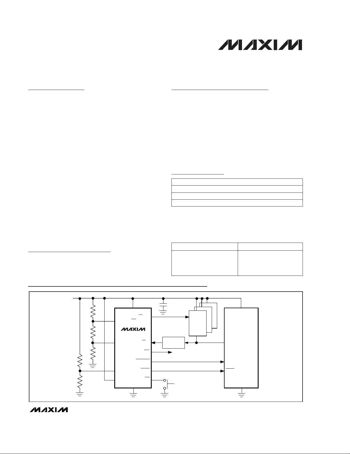
ADDRESS
DECODER
RESET IN/INT
LLIN/
REFOUT
OVI
SWT
3
V
CC
GND
12
MR
RESET
LOW LINE
OVO
CE IN
CE OUT
0.1µF
V
CC
RAM
A0-A15
V
CC
GND
NMI
RESET
µP
13
Typical Operating Circuit
PART** TEMP. RANGE PIN-PACKAGE
MAX792_CPE
0°C to +70°C 16 Plastic DIP
MAX792_CSE 0°C to +70°C 16 Narrow SO
MAX792_C/D 0°C to +70°C Dice*
SUFFIX
RESET THRESHOLD (V)
4.62
4.37
3.06
2.91
2.61
L
M
T
S
R
For free samples & the latest literature: http://www.maxim-ic.com, or phone 1-800-998-8800.
For small orders, phone 1-800-835-8769.
Ordering Information
MAX792/MAX820
Input Voltage (with respect to GND)
V
CC
.......................................................................-0.3V to +6V
All Other Inputs.......................................-0.3V to (V
CC
+ 0.3V)
Input Current
GND................................................................................25mA
All Other Outputs ............................................................25mA
Continuous Power Dissipation (TA= +70°C)
Plastic DIP (derate 10.53mW/°C above +70°C) ..........842mW
Narrow SO (derate 9.52mW/°C above +70°C) ............762mW
CERDIP (derate 10.00mW/°C above +70°C)...............800mW
Operating Temperature Ranges:
MAX792_C__/MAX820_C__................................0°C to +70°C
MAX792_E__/MAX820_E__ .............................-40°C to +85°C
MAX792_MJE__/MAX820_MJE__..................-55°C to +125°C
Storage Temperature Range.............................-65°C to +160°C
Lead Temperature (soldering, 10sec).............................+300°C
2 _______________________________________________________________________________________
Microprocessor and Non-Volatile
Memory Supervisory Circuits
PARAMETER
Reset Active Timeout Period
CONDITIONS
MAX820R, TA= +25°C, VCCfalling (Note 1) 2.55 2.66
MIN TYP MAX UNITS
VCCrising
MAX820S, TA= +25°C, VCCfalling 2.85 2.96
RESET Output Voltage
Reset Threshold Voltage—
Internal Threshold Mode
(VTH)
MAX820T, TA= +25°C, VCCfalling 3.00 3.11
V
140 200 280
MAX792, VCC= 5V or VCC= 3V 1.25 1.30 1.35
Reset Threshold Voltage
External Threshold Mode (VTH)
MAX820, VCC= 5V or VCC= 3V 1.274 1.30 1.326
V
RESET IN/INT Mode Threshold
(Note 2)
Internal threshold mode 60 mV
RESET IN/INT Leakage Current
±0.01 ±25 nA
Reset Threshold Hysteresis 0.016 x V
TH
V
Reset Comparator Delay VCCfalling 70 µs
ms
RESET Output Voltage
Operating Voltage Range
I
SINK
= 50µA, VCC= 1V, VCCfalling 0.01 0.3
I
SOURCE
= 1mA
2.65 V
Supply Current
VCC- 1
I
SINK
= 1.6mA 0.1 0.4
70 150 µA
I
SOURCE
= 100µA VCC- 0.5
I
SOURCE
= 1mA VCC- 1
V
MAX792L, MAX820L
I
SOURCE
= 100µA
4.50 4.62 4.75
VCC- 0.5
V
MAX792M, MAX820M 4.25 4.37 4.50
MAX792R, MAX820R
I
SINK
= 1.6mA
2.55 2.61 2.70
0.1 0.4
MAX792S, MAX820S 2.85 2.91 3.00
MAX792T, MAX820T 3.00 3.06 3.15
MAX820L, TA= +25°C, VCCfalling 4.55 4.70
MAX820M, TA= +25°C, VCCfalling 4.30 4.45
ELECTRICAL CHARACTERISTICS
(VCC= 2.65V to 5.5V, TA= T
MIN
to T
MAX
, unless otherwise noted.)
Stresses beyond those listed under “Absolute Maximum Ratings” may cause permanent damage to the device. These are stress ratings only, and functional
operation of the device at these or any other conditions beyond those indicated in the operational sections of the specifications is not implied. Exposure to
absolute maximum rating conditions for extended periods may affect device reliability.
ABSOLUTE MAXIMUM RATINGS
RESET COMPARATOR
MAX792/MAX820
_______________________________________________________________________________________ 3
Microprocessor and Non-Volatile
Memory Supervisory Circuits
ELECTRICAL CHARACTERISTICS (continued)
(VCC= 2.65V to 5.5V, TA= T
MIN
to T
MAX
, unless otherwise noted.)
PARAMETER
CONDITIONS
ms
MIN TYP MAX UNITS
µA
LOWLINE Short-Circuit Current
Output source current, VCC= 5.5V 10 50
SWT connected to V
CC, VCC = 5V
1.00 1.60 2.25
SWT connected to V
CC, VCC = 3V
1.00 1.60 2.25
4.7nF capacitor connected from SWT to GND
,
V
CC = 3V
70
Watchdog Timeout Period
4.7nF capacitor connected from SWT to GND
,
V
CC = 5V
MAX792/MAX820L/M
100
sec
50 120 210
Low-Line Threshold Voltage
(Internal Threshold Mode)—V
TH
MAX792/MAX820R/S/T
V
CC = 5V
40 100 210
mV
100
MAX792, VCC= 5V OR VCC= 3V
Watchdog Input Pulse Width VIL= 0V, VIH= V
CC
1.25 1.30 1.35
Low-Line Threshold Voltage
(External Programming Mode)
V
CC = 3V
MAX820, VCC= 5V OR VCC= 3V
300
ns
1.274 1.30 1.326
V
Low-Line Hysteresis
(Internal Threshold Mode)
I
SINK
= 50µA, VCC= 1V, VCCfalling
20 mV
0.01 0.30
I
SINK
= 1.6mA 0.1 0.4
I
SOURCE
= 1mA VCC- 1
WDO Output Voltage
I
SOURCE
= 100µA VCC- 0.5
V
I
SOURCE
= 100µA
WDPO to WDO Delay
70 ns
WDPO Duration
0.5 1.7 6.0 ms
I
SINK
= 50µA, VCC= 1V, VCCfalling 0.01 0.3
I
SINK
= 1.6mA 0.1 0.4
V
IH
I
SOURCE
= 1mA VCC- 1
WDPO Output Voltage
V
IL
VCC- 0.5
V
V
IH
0.75 x V
CC
V
IL
VCC= 4.25V
0.8
0.9 x V
CC
WDI Threshold Voltage
VCC= 2.55V
0.2
V
WDI Input Current ±1 µA
LLIN/REFOUT Leakage Current
External Programming Mode
±0.01 ±25 nA
Low-Line Comparator Delay VCCfalling 450 µs
I
SINK
= 3.2mA 0.4
LOWLINE Voltage
I
SOURCE
= 1µA VCC- 1
V
LOW-LINE COMPARATOR
WATCHDOG FUNCTION
MAX792/MAX820
4 _______________________________________________________________________________________
Microprocessor and Non-Volatile
Memory Supervisory Circuits
Note 1: The minimum operating voltage is 2.65V; however, the device is guaranteed to operate down to its preset reset threshold.
Note 2: Pulling RESET IN/INT below 60mV selects internal threshold mode and connects the internal voltage divider to the reset
and low-line comparators. External programming mode allows an external resistor divider to set the low-line and reset
thresholds (see Figure 4).
Note 3: The Chip-Enable Propagation delay is measured from the 50% point at CE IN to the 50% point at CE OUT.
PARAMETER
CONDITIONS
VCC= 5V or VCC= 3V
MIN TYP MAX UNITS
I
SINK
= 3.2mA
I
SOURCE
= 1µA
Output source current, VCC= 5.5V
VOD= 100mV, OVI rising
MR Pull-Up Current
V
IH
0.75 x V
CC
MR = 0V
VCC= 2.5V
V
CC
= 4.25V
V
IL
0.8
1
V
IH
0.75 x V
CC
CE IN Threshold Voltage
VCC= 2.55V
V
IL
0.2
V
CE IN Leakage Current
50Ω source impedance driver,
C
LOAD
= 50pF
Disabled mode ±0.005 ±1 µA
VCC= 5V
VCC= 3V
VCC= 5V 75 150
610
CE IN to CE OUT Resistance
OVI Input Threshold
Enabled mode
VCC= 3V 150 300
1.25 1.30 1.35 V
OVI Leakage Current
Ω
±0.01 ±25 nA
VCC= 5V 0.5 2.5
CE OUT Short-Circuit Current
0.4
OVO Output Voltage
Disabled mode, CE
OUT
= 0V
VCC= 3V 0.05 0.2 0.4
VCC- 1
V
mA
Chip-Enable Propagation Delay
(Note 3)
10 50
813
ns
I
OUT
= -100µA VCC- 1
Chip-Enable Output Voltage
High (Reset Active)
I
OUT
= 10µA VCC- 0.5
V
Reset Active to CE OUT High
V
CC
falling 15 µs
MR Minimum Pulse Width
25 µs
MR to RESET Propagation Delay
12 µs
MR Threshold Range
1.1 1.3 1.5 V
VCC= 4.25V
to VCC= 5.5V
52380
µA
OVO Short-Circuit Current
µA
13
OVI to OVO Delay
VOD= 100mV, OVI falling 55
µs
ELECTRICAL CHARACTERISTICS (continued)
(VCC= 2.65V to 5.5V, TA= T
MIN
to T
MAX
, unless otherwise noted.)
MANUAL RESET
CHIP-ENABLE GATING
OVERVOLTAGE COMPARATOR
MAX792/MAX820
Microprocessor and Non-Volatile
Memory Supervisory Circuits
_________________________________________________________________________________________________
5
400
-60
LOW-LINE COMPARATOR
PROPAGATION DELAY vs. TEMPERATURE
100
300
200
MAX792-3a
TEMPERATURE (°C)
PROPAGATION DELAY (µs)
500
600
-30 0 30 60 90 120
150
V
CC
= 5V
V
CC
= 3V
V
CC
FALLING
15mV OVERDRIVE
EXTERNAL PROGRAMMING MODE
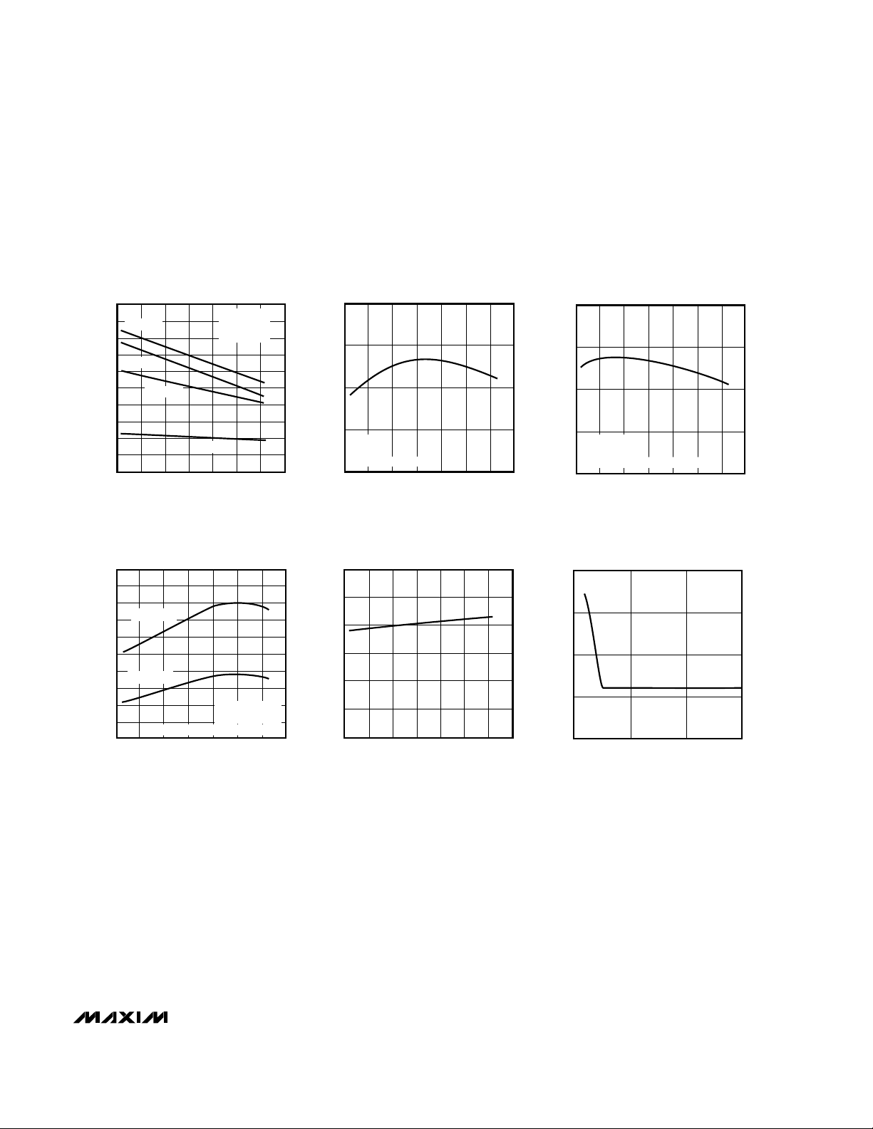
__________________________________________Typical Operating Characteristics
(TA = +25°C, unless otherwise noted.)
80
0
-60 150
SUPPLY CURRENT vs. TEMPERATURE
20
60
MAX792-1
TEMPERATURE (°C)
SUPPLY CURRENT (µA)
40
10
30
50
70
90
100
-30 0 30 60 90 120
V
CC
= 2V
VCC = 3V
VCC = 4V
VCC = 5V
SWT = VCC
ALL OUTPUTS
UNLOADED
50
40
-60
OVERVOLTAGE COMPARATOR
PROPAGATION DELAY vs. TEMPERATURE
30
MAX792-2
TEMPERATURE (°C)
PROPAGATION DELAY (µs)
60
70
-30 0 30 60 90 120
150
VIH TO V
OL
VIN = 20mV
OVERDRIVE = 15mV
40
-60
RESET COMPARATOR
PROPAGATION DELAY vs. TEMPERATURE
50
MAX792-3
TEMPERATURE (°C)
PROPAGATION DELAY (µs)
60
70
60
80
-30 0 30 90 120
150
VCC FALLING
15mV OVERDRIVE
EXTERNAL PROGRAMMING MODE
0
-60
POWER-UP RESET DELAY
vs. TEMPERATURE
100
MAX792-4
TEMPERATURE (°C)
DELAY (ms)
60
300
200
50
150
250
-30 0 30 90 120
150
1.0
NOMINAL WATCHDOG TIMEOUT
PERIOD vs. V
CC
MAX792-5
VCC (V)
NOMINAL WATCHDOG TIMEOUT PERIOD (sec)
4
3.0
2.0
2
3
5
1.5
2.5
 Loading...