

MAX792/MAX820
Microprocessor and Non-Volatile
Memory Supervisory Circuits
________________________________________________________________
Maxim Integrated Products
1
19-0147; Rev. 2; 6/98
General Description
The MAX792/MAX820 microprocessor (µP) supervisory
circuits provide the most functions for power-supply
and watchdog monitoring in systems without battery
backup. Built-in features include the following:
1) µP reset: Assertion of RESET and
RESET
outputs during power-up, power-down, and brownout conditions.
RESET
is guaranteed valid for VCCdown to 1V.
2) Manual-reset input.
3) Two-stage power-fail warning: A separate low-line
comparator compares VCCto a preset threshold
120mV above the reset threshold; the low-line and
reset thresholds can be programmed externally.
4) Watchdog fault output: Assertion of
WDO
if the watchdog input is not toggled within a preset timeout
period.
5) Pulsed watchdog output: Advance warning of
impending
WDO
assertion from watchdog timeout
that causes hardware shutdown.
6) Write protection of CMOS RAM, EEPROM, or other
memory devices.
The MAX792 and MAX820 are identical, except the
MAX820 guarantees higher low-line and reset threshold
accuracy (±2%).
Applications
Computers
Controllers
Intelligent Instruments
Critical µP Power Monitoring
Features
♦ Manual-Reset Input
♦ 200ms Power-OK/Reset Time Delay
♦ Independent Watchdog Timer—Preset or Adjustable
♦ On-Board Gating of Chip-Enable Signals
♦ Memory Write-Cycle Completion
♦ 10ns (max) Chip-Enable Gate Propagation Delay
♦ Voltage Monitor for Overvoltage Warning
♦ ±2% Reset and Low-Line Threshold Accuracy
(MAX820, external programming mode)
Ordering Information continued at end of data sheet.
* Dice are tested at T
A
= +25°C, DC parameters only.
**These parts offer a choice of five different reset threshold voltages. Select the letter corresponding to the desired nominal
reset threshold voltage and insert it into the blank to complete the
part number.
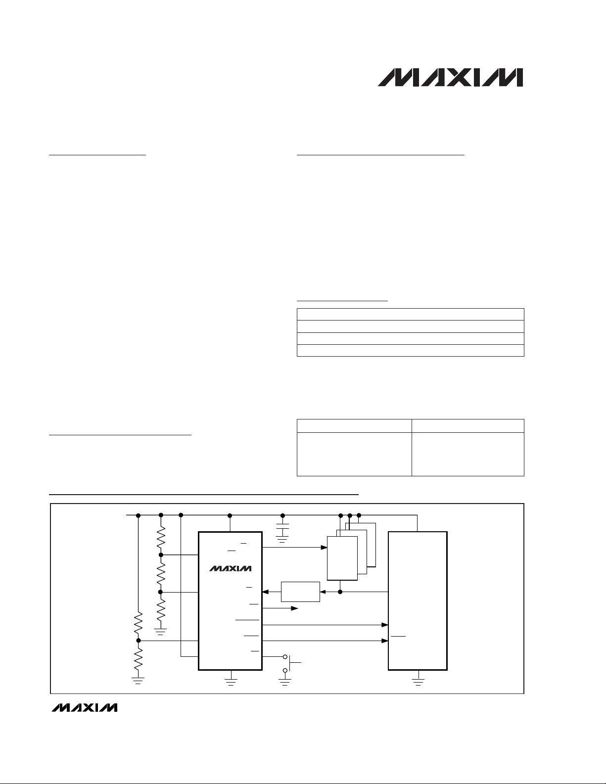
MAX792
4
5
7
8
9
1
10
6
14
ADDRESS
DECODER
RESET IN/INT
LLIN/
REFOUT
OVI
SWT
3
V
CC
GND
12
MR
RESET
LOW LINE
OVO
CE IN
CE OUT
0.1µF
V
CC
RAM
A0-A15
V
CC
GND
NMI
RESET
µP
13
Typical Operating Circuit
PART** TEMP. RANGE PIN-PACKAGE
MAX792_CPE
0°C to +70°C 16 Plastic DIP
MAX792_CSE 0°C to +70°C 16 Narrow SO
MAX792_C/D 0°C to +70°C Dice*
SUFFIX
RESET THRESHOLD (V)
4.62
4.37
3.06
2.91
2.61
L
M
T
S
R
For free samples & the latest literature: http://www.maxim-ic.com, or phone 1-800-998-8800.
For small orders, phone 1-800-835-8769.
Ordering Information
MAX792/MAX820
Input Voltage (with respect to GND)
V
CC
.......................................................................-0.3V to +6V
All Other Inputs.......................................-0.3V to (V
CC
+ 0.3V)
Input Current
GND................................................................................25mA
All Other Outputs ............................................................25mA
Continuous Power Dissipation (TA= +70°C)
Plastic DIP (derate 10.53mW/°C above +70°C) ..........842mW
Narrow SO (derate 9.52mW/°C above +70°C) ............762mW
CERDIP (derate 10.00mW/°C above +70°C)...............800mW
Operating Temperature Ranges:
MAX792_C__/MAX820_C__................................0°C to +70°C
MAX792_E__/MAX820_E__ .............................-40°C to +85°C
MAX792_MJE__/MAX820_MJE__..................-55°C to +125°C
Storage Temperature Range.............................-65°C to +160°C
Lead Temperature (soldering, 10sec).............................+300°C
2 _______________________________________________________________________________________
Microprocessor and Non-Volatile
Memory Supervisory Circuits
PARAMETER
Reset Active Timeout Period
CONDITIONS
MAX820R, TA= +25°C, VCCfalling (Note 1) 2.55 2.66
MIN TYP MAX UNITS
VCCrising
MAX820S, TA= +25°C, VCCfalling 2.85 2.96
RESET Output Voltage
Reset Threshold Voltage—
Internal Threshold Mode
(VTH)
MAX820T, TA= +25°C, VCCfalling 3.00 3.11
V
140 200 280
MAX792, VCC= 5V or VCC= 3V 1.25 1.30 1.35
Reset Threshold Voltage
External Threshold Mode (VTH)
MAX820, VCC= 5V or VCC= 3V 1.274 1.30 1.326
V
RESET IN/INT Mode Threshold
(Note 2)
Internal threshold mode 60 mV
RESET IN/INT Leakage Current
±0.01 ±25 nA
Reset Threshold Hysteresis 0.016 x V
TH
V
Reset Comparator Delay VCCfalling 70 µs
ms
RESET Output Voltage
Operating Voltage Range
I
SINK
= 50µA, VCC= 1V, VCCfalling 0.01 0.3
I
SOURCE
= 1mA
2.65 V
Supply Current
VCC- 1
I
SINK
= 1.6mA 0.1 0.4
70 150 µA
I
SOURCE
= 100µA VCC- 0.5
I
SOURCE
= 1mA VCC- 1
V
MAX792L, MAX820L
I
SOURCE
= 100µA
4.50 4.62 4.75
VCC- 0.5
V
MAX792M, MAX820M 4.25 4.37 4.50
MAX792R, MAX820R
I
SINK
= 1.6mA
2.55 2.61 2.70
0.1 0.4
MAX792S, MAX820S 2.85 2.91 3.00
MAX792T, MAX820T 3.00 3.06 3.15
MAX820L, TA= +25°C, VCCfalling 4.55 4.70
MAX820M, TA= +25°C, VCCfalling 4.30 4.45
ELECTRICAL CHARACTERISTICS
(VCC= 2.65V to 5.5V, TA= T
MIN
to T
MAX
, unless otherwise noted.)
Stresses beyond those listed under “Absolute Maximum Ratings” may cause permanent damage to the device. These are stress ratings only, and functional
operation of the device at these or any other conditions beyond those indicated in the operational sections of the specifications is not implied. Exposure to
absolute maximum rating conditions for extended periods may affect device reliability.
ABSOLUTE MAXIMUM RATINGS
RESET COMPARATOR
MAX792/MAX820
_______________________________________________________________________________________ 3
Microprocessor and Non-Volatile
Memory Supervisory Circuits
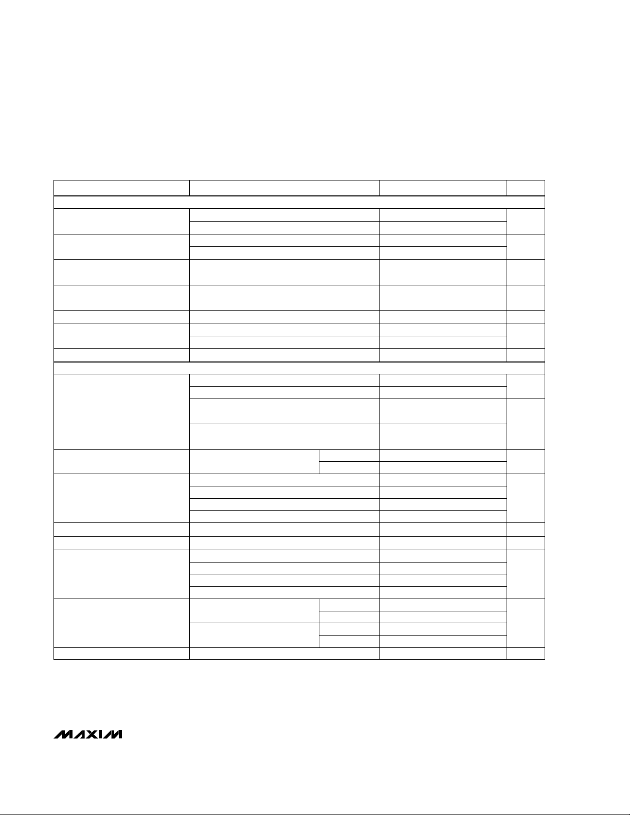
ELECTRICAL CHARACTERISTICS (continued)
(VCC= 2.65V to 5.5V, TA= T
MIN
to T
MAX
, unless otherwise noted.)
PARAMETER
CONDITIONS
ms
MIN TYP MAX UNITS
µA
LOWLINE Short-Circuit Current
Output source current, VCC= 5.5V 10 50
SWT connected to V
CC, VCC = 5V
1.00 1.60 2.25
SWT connected to V
CC, VCC = 3V
1.00 1.60 2.25
4.7nF capacitor connected from SWT to GND
,
V
CC = 3V
70
Watchdog Timeout Period
4.7nF capacitor connected from SWT to GND
,
V
CC = 5V
MAX792/MAX820L/M
100
sec
50 120 210
Low-Line Threshold Voltage
(Internal Threshold Mode)—V
TH
MAX792/MAX820R/S/T
V
CC = 5V
40 100 210
mV
100
MAX792, VCC= 5V OR VCC= 3V
Watchdog Input Pulse Width VIL= 0V, VIH= V
CC
1.25 1.30 1.35
Low-Line Threshold Voltage
(External Programming Mode)
V
CC = 3V
MAX820, VCC= 5V OR VCC= 3V
300
ns
1.274 1.30 1.326
V
Low-Line Hysteresis
(Internal Threshold Mode)
I
SINK
= 50µA, VCC= 1V, VCCfalling
20 mV
0.01 0.30
I
SINK
= 1.6mA 0.1 0.4
I
SOURCE
= 1mA VCC- 1
WDO Output Voltage
I
SOURCE
= 100µA VCC- 0.5
V
I
SOURCE
= 100µA
WDPO to WDO Delay
70 ns
WDPO Duration
0.5 1.7 6.0 ms
I
SINK
= 50µA, VCC= 1V, VCCfalling 0.01 0.3
I
SINK
= 1.6mA 0.1 0.4
V
IH
I
SOURCE
= 1mA VCC- 1
WDPO Output Voltage
V
IL
VCC- 0.5
V
V
IH
0.75 x V
CC
V
IL
VCC= 4.25V
0.8
0.9 x V
CC
WDI Threshold Voltage
VCC= 2.55V
0.2
V
WDI Input Current ±1 µA
LLIN/REFOUT Leakage Current
External Programming Mode
±0.01 ±25 nA
Low-Line Comparator Delay VCCfalling 450 µs
I
SINK
= 3.2mA 0.4
LOWLINE Voltage
I
SOURCE
= 1µA VCC- 1
V
LOW-LINE COMPARATOR
WATCHDOG FUNCTION
MAX792/MAX820
4 _______________________________________________________________________________________
Microprocessor and Non-Volatile
Memory Supervisory Circuits
Note 1: The minimum operating voltage is 2.65V; however, the device is guaranteed to operate down to its preset reset threshold.
Note 2: Pulling RESET IN/INT below 60mV selects internal threshold mode and connects the internal voltage divider to the reset
and low-line comparators. External programming mode allows an external resistor divider to set the low-line and reset
thresholds (see Figure 4).
Note 3: The Chip-Enable Propagation delay is measured from the 50% point at CE IN to the 50% point at CE OUT.
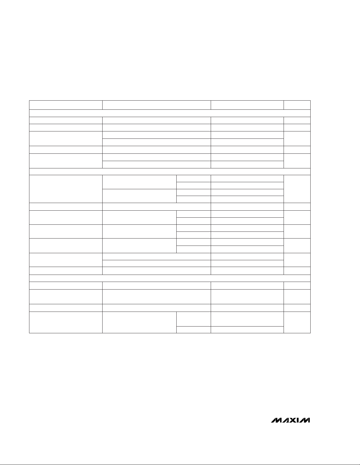
PARAMETER
CONDITIONS
VCC= 5V or VCC= 3V
MIN TYP MAX UNITS
I
SINK
= 3.2mA
I
SOURCE
= 1µA
Output source current, VCC= 5.5V
VOD= 100mV, OVI rising
MR Pull-Up Current
V
IH
0.75 x V
CC
MR = 0V
VCC= 2.5V
V
CC
= 4.25V
V
IL
0.8
1
V
IH
0.75 x V
CC
CE IN Threshold Voltage
VCC= 2.55V
V
IL
0.2
V
CE IN Leakage Current
50Ω source impedance driver,
C
LOAD
= 50pF
Disabled mode ±0.005 ±1 µA
VCC= 5V
VCC= 3V
VCC= 5V 75 150
610
CE IN to CE OUT Resistance
OVI Input Threshold
Enabled mode
VCC= 3V 150 300
1.25 1.30 1.35 V
OVI Leakage Current
Ω
±0.01 ±25 nA
VCC= 5V 0.5 2.5
CE OUT Short-Circuit Current
0.4
OVO Output Voltage
Disabled mode, CE
OUT
= 0V
VCC= 3V 0.05 0.2 0.4
VCC- 1
V
mA
Chip-Enable Propagation Delay
(Note 3)
10 50
813
ns
I
OUT
= -100µA VCC- 1
Chip-Enable Output Voltage
High (Reset Active)
I
OUT
= 10µA VCC- 0.5
V
Reset Active to CE OUT High
V
CC
falling 15 µs
MR Minimum Pulse Width
25 µs
MR to RESET Propagation Delay
12 µs
MR Threshold Range
1.1 1.3 1.5 V
VCC= 4.25V
to VCC= 5.5V
52380
µA
OVO Short-Circuit Current
µA
13
OVI to OVO Delay
VOD= 100mV, OVI falling 55
µs
ELECTRICAL CHARACTERISTICS (continued)
(VCC= 2.65V to 5.5V, TA= T
MIN
to T
MAX
, unless otherwise noted.)
MANUAL RESET
CHIP-ENABLE GATING
OVERVOLTAGE COMPARATOR
MAX792/MAX820
Microprocessor and Non-Volatile
Memory Supervisory Circuits
_________________________________________________________________________________________________
5
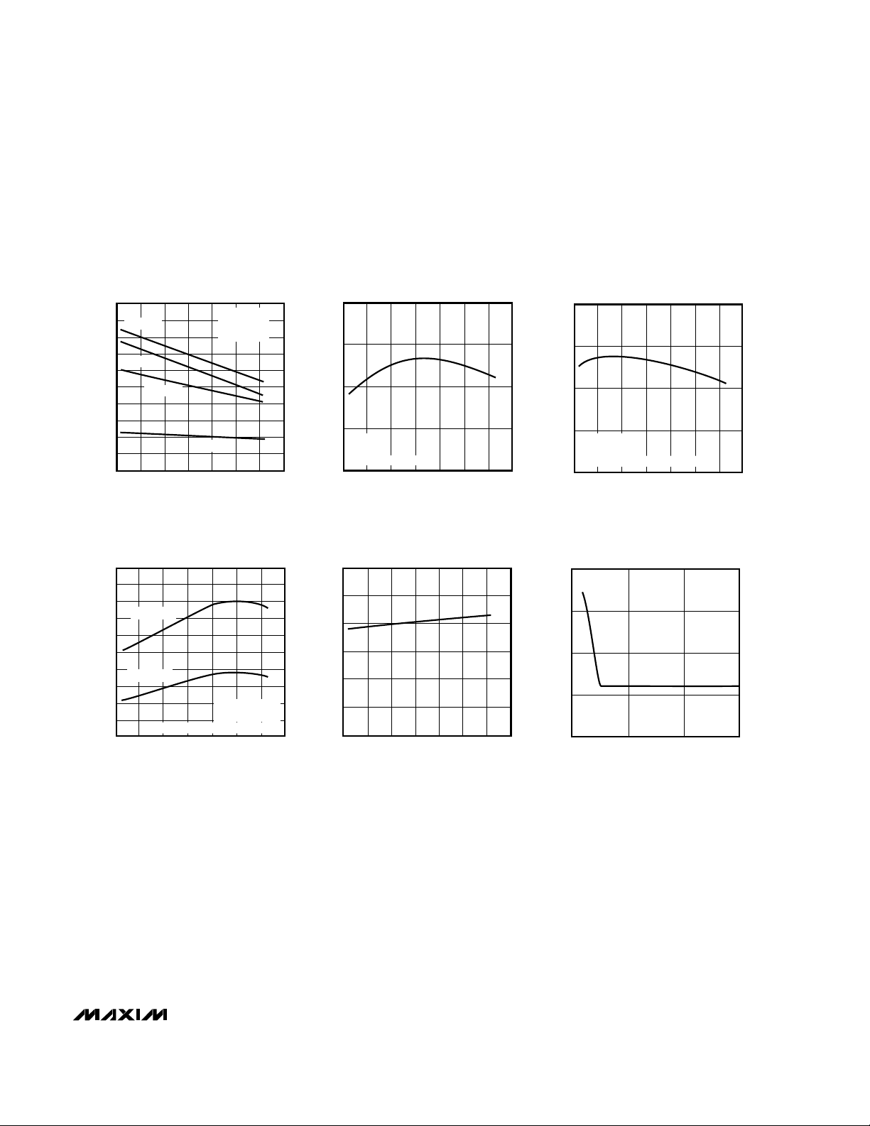
400
-60
LOW-LINE COMPARATOR
PROPAGATION DELAY vs. TEMPERATURE
100
300
200
MAX792-3a
TEMPERATURE (°C)
PROPAGATION DELAY (µs)
500
600
-30 0 30 60 90 120
150
V
CC
= 5V
V
CC
= 3V
V
CC
FALLING
15mV OVERDRIVE
EXTERNAL PROGRAMMING MODE
__________________________________________Typical Operating Characteristics
(TA = +25°C, unless otherwise noted.)
80
0
-60 150
SUPPLY CURRENT vs. TEMPERATURE
20
60
MAX792-1
TEMPERATURE (°C)
SUPPLY CURRENT (µA)
40
10
30
50
70
90
100
-30 0 30 60 90 120
V
CC
= 2V
VCC = 3V
VCC = 4V
VCC = 5V
SWT = VCC
ALL OUTPUTS
UNLOADED
50
40
-60
OVERVOLTAGE COMPARATOR
PROPAGATION DELAY vs. TEMPERATURE
30
MAX792-2
TEMPERATURE (°C)
PROPAGATION DELAY (µs)
60
70
-30 0 30 60 90 120
150
VIH TO V
OL
VIN = 20mV
OVERDRIVE = 15mV
40
-60
RESET COMPARATOR
PROPAGATION DELAY vs. TEMPERATURE
50
MAX792-3
TEMPERATURE (°C)
PROPAGATION DELAY (µs)
60
70
60
80
-30 0 30 90 120
150
VCC FALLING
15mV OVERDRIVE
EXTERNAL PROGRAMMING MODE
0
-60
POWER-UP RESET DELAY
vs. TEMPERATURE
100
MAX792-4
TEMPERATURE (°C)
DELAY (ms)
60
300
200
50
150
250
-30 0 30 90 120
150
1.0
NOMINAL WATCHDOG TIMEOUT
PERIOD vs. V
CC
MAX792-5
VCC (V)
NOMINAL WATCHDOG TIMEOUT PERIOD (sec)
4
3.0
2.0
2
3
5
1.5
2.5

MAX792/MAX820
Microprocessor and Non-Volatile
Memory Supervisory Circuits
6
_______________________________________________________________________________________
____________________________Typical Operating Characteristics (continued)
(TA = +25°C, unless otherwise noted.)
100k
10
1n 1m
WATCHDOG TIMEOUT PERIOD
vs. SWT LOAD CAPACITANCE
1k
10k
MAX792-10
C
SWT
(F)
WATCHDOG TIMEOUT PERIOD (ms)
10n 100n
100
VCC = 5V
VCC = 3V
20
0
0 25 125 250
CHIP-ENABLE PROPAGATION DELAY
vs. CE OUT LOAD CAPACITANCE
5
15
MAX792-11
C
LOAD
(pF)
PROPAGATION DELAY (ns)
75 200
10
50 100 150 175 225
VCC = +5V
V
CE IN
= 0V TO 5V
DRIVER SOURCE
IMPEDANCE = 50Ω
1.25
0 120
REF OUT VOLTAGE
vs. TEMPERATURE
MAX792-7
TEMPERATURE (°C)
REF OUT (V)
1.26
1.27
1.28
1.29
1.30
1.31
1.32
1.33
150
906030-30-60
RESET IN / INT = 0V
160
20
0 60 120
CHIP-ENABLE ON-RESISTANCE
vs. TEMPERATURE
40
120
MAX792-8
TEMPERATURE (°C)
ON-RESISTANCE (Ω)
80
180
200
60
100
140
90 15030-30-60
VCC = 5V
V
CE IN
= 2.5V
0
VCC = 3V
V
CE IN
= 1.5V
0.900
0 60 150
INTERNAL-MODE RESET THRESHOLD
vs. TEMPERATURE (NORMALIZED)
MAX792-6
TEMPERATURE (°C)
RESET THRESHOLD
1209030-30-60
0.925
0.950
1.000
1.025
1.050
1.075
1.100
1.125
0.975
THE RESET THRESHOLD IS SHOWN
NORMALIZED TO 1, REPRESENTING
ALL AVAILABLE MAX792/MAX820

MAX792/MAX820
Microprocessor and Non-Volatile
Memory Supervisory Circuits
_______________________________________________________________________________________ 7
______________________________________________________________Pin Description
PIN NAME FUNCTION
1
RESET
2 RESET
Reset is the inverse of RESET.
3V
CC
Input Supply Voltage
4
RESET IN/INT
5 LLIN/REF OUT
6
OVO
7 OVI
8 SWT
9
MR
10
LOW LINE
11 WDI
12 GND Ground
13
CE OUT
Active-Low Reset Output goes low whenever V
CC
falls below the reset threshold in internal threshold programming mode, or RESET IN falls below 1.30V in external threshold programming mode.
RESET remains low for 200ms typ after the threshold is exceeded on power-up.
Reset-Input/Internal-Mode Select. Connect this input to GND to select internal threshold mode.
Select external programming mode by pulling this input 600mV or higher through an external voltage divider.
Low-Line Input/Reference Output connects directly to the low-line comparator in external programming mode (RESET IN/INT ≥ 600mV). Connects directly to the internal 1.30V reference in internal
threshold mode (RESET IN/INT
≤ 60mV).
Overvoltage Comparator Output goes low when OVI is greater than 1.30V. This is an uncommitted
comparator and has no effect on any other internal circuitry.
Inverting Input to the Overvoltage Comparator. When OVI is greater than 1.30V, OVO goes low.
Connect OVI to GND or V
CC
when not used.
Set Watchdog-Timeout Input. Connect this input to V
CC
to select the default 1.6sec watchdog
timeout period. Connect a capacitor between this input and GND to select another watchdogtimeout period. Watchdog timeout period = k x (capacitor value in nF)mV, where k = 27 for
VCC= 5V and k = 16.2 for VCC= 3V. If the watchdog function is unused, connect SWT to VCC.
16
WDPO
15
WDO
14
CE IN
Manual-Reset Input. This input can be tied to an external momentary pushbutton switch, or to a
logic gate output. Internally pulled up to V
CC
.
Low-Line Output. LOW LINE goes low 120mV above the reset threshold in internal threshold mode,
or when LLIN/REFOUT goes below 1.30V in external programming mode.
Watchdog Input. If WDI remains either high or low for longer than the watchdog timeout period,
WDPO pulses low and WDO goes low. WDO remains low until the next transition at WDI. Connect to
GND or V
CC
if unused.
Chip-Enable Output. CE OUT goes low only when CE IN is low and reset is not asserted. If CE IN is
low when reset is asserted, CE OUT will stay low for 15µs or until CE IN goes high, whichever
occurs first.
Chip-Enable Input—the input to the chip-enable transmission gate. Connect to GND or VCCif not
used.
Watchdog Output. WDO goes low if WDI remains either high or low longer than the watchdog timeout period. WDO returns high on the next transition at WDI.
Watchdog-Pulse Output. Upon the absence of a transition at WDI, WDPO will pulse low for a minimum of 500µs. WDPO precedes WDO by typically 70ns.

MAX792/MAX820
Microprocessor and Non-Volatile
Memory Supervisory Circuits
8 _______________________________________________________________________________________
Detailed Description
Manual-Reset Input
Many µP-based products require manual-reset capability, allowing the operator to initiate a reset. The manual/external-reset input (
MR) ca
n connect directly to a
switch without an external pull-up resistor or debouncing network. MRinternally connects to a 1.30V comparator, and has a high-impedance pull-up to VCC, as
shown in Figure 1. The propagation delay from asserting MRto reset asserted is typically 12µs. Pulsing
MR
low for a minimum of 25µs asserts the reset function
(see
Reset Function
section). The reset output remains
active as long as MRis held low, and the reset timeout
period begins after MRreturns high (Figure 2). To provide extra noise immunity in high-noise environments,
pull MRup to VCCwith a 100kΩ resistor.
Use MRas either a digital logic input or as a second lowline comparator. Normal TTL/CMOS levels can be
wire-OR connected via pull-down diodes (Figure 3),
and open-drain/collector outputs can be wire-ORed
directly.
Monitoring the Regulated Supply
The MAX792/MAX820 offer two modes for monitoring
the regulated supply and providing reset and nonmaskable interrupt (NMI) signals to the µP: internal
threshold mode uses the factory preset low-line and
reset thresholds, and external programming mode
allows the low-line and reset thresholds to be programmed externally using a resistor voltage divider
(Figure 4).
Internal Threshold Mode
Connecting the reset-input/internal-mode select pin
(RESET IN
/INT
) to ground selects internal threshold
mode (Figure 4a). In this mode, the low-line and reset
thresholds are factory preset by an internal voltage
divider (Figure 1) to the threshold voltages specified in
the
Electrical Characteristics
(Reset Threshold Voltage
and Low-Line Threshold Voltage). Connect the low-line
output (
LOWLINE
) to the µP NMI pin, and connect the
active-high reset output (RESET) or active-low reset
output
(RESET
) to the µP reset input pin.
Additionally, the low-line input/reference-output pin
(LLIN/REFOUT) connects to the internal 1.30V reference in internal threshold mode. Buffer LLIN/REFOUT
with a high-impedance buffer to use it with external
circuitry. In this mode, when VCCis falling,
LOWLINE
is
guaranteed to be asserted prior to reset assertion.
External Programming Mode
Connecting RESET IN
/INT
to a voltage above 600mV
selects external programming mode. In this mode, the
low-line and reset comparators disconnect from the internal voltage divider and connect to LLIN/REFOUT and
RESET IN
/INT
, respectively (Figure 1). This mode allows
flexibility in determining where in the operating voltage
range the NMI and reset are generated. Set the low-line
and reset thresholds with an external resistor divider, as in
Figure 4b or Figure 4c. RESET typically remains valid for
VCCdown to 2.5V;
RESET
is guaranteed to be valid with
VCCdown to 1V.
Calculate the values for the resistor voltage divider in
Figure 4b using the following equations:
1) R3 = (1.30 x VCCMAX)/(V
LOW LINE
x I
MAX
)
2) R2 = [(1.30 x VCCMAX)/(V
RESET
x I
MAX
)] - R3
3) R1 = (VCCMAX/I
MAX
) - (R2 + R3).
First choose the desired maximum current through the
voltage divider (I
MAX
) when VCCis at its highest (V
CC
MAX). There are two things to consider here. First, I
MAX
contributes to the overall supply current for the circuit, so
you would generally make it as small as possible.
Second, I
MAX
cannot be too small or leakage currents will
adversely affect the programmed threshold voltages; 5µA
is often appropriate. Determine R3 after you have chosen
I
MAX
. Use the value for R3 to determine R2, then use both
R2 and R3 to determine R1.
For example, to program a 4.75V low-line threshold and a
4.4V reset threshold, first choose I
MAX
to be 5µA when
VCC= 5.5V and substitute into equation 1.
R3 = (1.30 x 5.5)/(4.75 x 5E-6) = 301.05kΩ.
301kΩ is the nearest standard 0.1% value. Substitute
into equation 2:
R2 = [(1.30 x 5.5)/(4.4 x 5E-6)] - 301kΩ = 23.95kΩ.
The nearest 0.1% resistor value is 23.7kΩ. Finally, substitute into equation 3:
R1 = (5.5/5E-6) - (23.7kΩ + 301kΩ) = 775kΩ.
The nearest 0.1% value resistor is 787kΩ. Determine the
actual low-line threshold by rearranging equation 1 and
plugging in the standard resistor values. The actual lowline threshold is 4.75V and the actual reset threshold is
4.40V. An additional resistor allows the MAX792/MAX820
to monitor the unregulated supply and provide an NMI
before the regulated supply begins to fall (Figure 4c).
Both of these thresholds will vary from circuit to circuit
with resistor tolerance, reference variation, and comparator offset variation. The initial thresholds for each circuit
will also vary with temperature due to reference and offset drift. For highest accuracy, use the MAX820.

MAX792/MAX820
Microprocessor and Non-Volatile
Memory Supervisory Circuits
_______________________________________________________________________________________ 9
MAX792
MAX820
INTERNAL/
EXTERNAL
MODE
CONTROL
CHIP-ENABLE
OUTPUT
CONTROL
RESET
GENERATOR
TIMEBASE FOR
RESET AND
WATCHDOG
V
CC
WATCHDOG
TIMER
WATCHDOG
TRANSITION
DETECTOR
OVERVOLTAGE
COMPARATOR
P
N
INTERNAL
EXTERNAL
60mV
V
CC
V
CC
V
CC
1.30V
LOW-LINE
COMPARATOR
MANUAL
RESET
COMPARATOR
RESET
COMPARATOR
V
CC
V
CC
P
V
CC
*
4
5
9
14
8
11
7
6
15
16
13
10
1
2
3
RESET
RESET
LOW LINE
CE OUT
WDPO
WDO
OVO
12
GND
OVI
WDI
SWT
CE IN
MR
LLIN/
REFOUT
RESET IN/
INT
V
CC
* SWITCHES ARE SHOWN IN INTERNAL
THRESHOLD MODE POSITION
Figure 1. Block Diagram

MAX792/MAX820
Microprocessor and Non-Volatile
Memory Supervisory Circuits
10 ______________________________________________________________________________________
Low-Line Output
In internal threshold mode, the low-line comparator
monitors VCCwith a threshold voltage typically 120mV
above the reset threshold, and with 15mV of hysteresis.
For normal operation (VCCabove the reset threshold),
LOWLINE
is pulled to VCC. Use
LOWLINE
to provide an NMI
to the µP, as described in the previous section, when
VCCbegins to fall (Figure 4).
Reset Function
The MAX792/MAX820 provide both RESET and
RESET
outputs. The RESET and
RESET
outputs ensure that the
µP powers up in a known state, and prevent code-execution errors during power-up, power-down, or
brownout conditions.
The reset function will be asserted during the following
conditions:
1) VCCless than the programmed reset threshold.
2)MRless than 1.30V typ.
3) Reset remains asserted for 200ms typ after V
CC
rises above the reset threshold or after MRhas
exceeded 1.30V typ.
When reset is asserted, all the internal counters are
reset, the watchdog output (
WDO)
and watchdog-pulse
output
(WDPO)
are set high, and the set watchdog-timeout input (SWT) is set to (VCC- 0.6V) if it is not already
connected to VCC(for internal timeouts). The chipenable transmission gate is also disabled while reset is
asserted; the chip-enable input (CEIN) becomes high
impedance and the chip-enable output (CEOUT) is
pulled up to VCC.
MR
RESET
CE IN OV
CE OUT
25µs MIN
12µs TYP
15µs TYP
Figure 2. Manual-Reset Timing Diagram
MAX792
MAX820
MANUAL RESET
OTHER
RESET
SOURCES
9
MR
*
*
*
.
.
.
DIODES NOT REQUIRED ON OPEN-DRAIN OUTPUTS
Figure 3. Diode "OR" connections allow multiple reset sources
to connect to
MR.
MAX792
12
GND
3
V
CC
LLIN/REFOUT
RESET
RESET
LOW LINE
RESET IN/INT
4
5
2
10
1
TO µP
TO µP
TO µP NMI
V
IN
Figure 4a. Connection for Internal Threshold Mode
MAX792
GND
V
CC
TO µP
TO µP
TO µP NMI
2
1
10
RESET IN/INT
LLIN/REFOUT
RESET
RESET
LOW LINE
12
V
IN
R3 = 1.30V x VCC
MAX
V
LOW LINE
x I
MAX
R2 = 1.30V x VCC
MAX
V
RESET
x I
MAX
–
R3
R1 = V
CC MAX
I
MAX
– (R2 + R3)
I
MAX
= THE MAXIMUM DESIRED CURRENT
THROUGH THE VOLTAGE DIVIDED.
3
R3
R2
R1
Figure 4b. Connection for External Threshold Programming Mode

MAX792/MAX820
Microprocessor and Non-Volatile
Memory Supervisory Circuits
______________________________________________________________________________________ 11
Reset Outputs (RESET and RESET)
The
RESET
output is active low and typically sinks 1.6mA
at 0.1V. When deasserted,
RESET
sources 1.6mA at typi-
cally V
CC
- 1.5V. The RESET output is the inverse of
RESET. RESET
is guaranteed to be valid down to VCC= 1V,
and an external 10kΩ pull-down resistor on
RESET
ensures that it will be valid with VCCdown to GND
(Figure 5). As VCCgoes below 1V, the gate drive to the
RESET
output switch reduces accordingly, increasing the
r
DS(ON)
and the saturation voltage. The 10kΩ pull-down
resistor ensures that the parallel combination of switch
plus resistor will be around 10kΩ and the saturation
voltage will be below 0.4V while sinking 40µA. When
using an external pull-down resistor of 10kΩ, the high
state for the
RESET
output with VCC= 4.75V is typically
4.60V.
Overvoltage Comparator
The overvoltage comparator is an uncommitted comparator that has no effect on the operation of other chip
functions. Use this input to provide overvoltage indication by connecting a voltage divider from the input supply, as in Figure 6.
Connect OVI to ground if the overvoltage function is not
used.
OVO
goes low when OVI goes above 1.30V. With
OVI below 1.30V,
OVO
is actively pulled to VCCand can
source1µA.
Watchdog Function
The watchdog monitors µP activity via the watchdog
input (WDI). If the µP becomes inactive,
WDO
and
WDPO
are asserted. To use the watchdog function, connect
WDI to a µP bus line or I/O line. If WDI remains high or
low for longer than the watchdog timeout period
(1.6sec nominal),
WDPO
and
WDO
are asserted, indicat-
ing a software fault condition (see
Watchdog-Pulse
Output
and
Watchdog Output
sections).
Watchdog Input
If the watchdog function is unused, connect WDI to V
CC
or GND. A change of state (high-to-low, low-to-high, or
a minimum 100ns pulse) at WDI during the watchdog
period resets the watchdog timer. The watchdog timer
MAX792
MAX820
GND
V
CC
REGULATOR
R1
R2
R3
R4
TO µP
TO µP
TO µP NMI
2
1
10
RESET IN/INT
LLIN/REFOUT
RESET
RESET
LOW LINE
V
LOW LINE
= 1.3 R1 + R2
R2
)
(
V
RESET
= 1.3 R3 + R4
R4
)
(
Figure 4c. Alternative Connection for External Programming Mode
RESET
MAX792
MAX820
TO µP RESET
1
10k
Figure 5. Adding an external pull-down resistor ensures RESET
is valid with V
CC
down to GND.
MAX792
MAX820
6
7
12
GND
3
V
CC
OVI
OVO
OVERVOLTAGE
VOLTAGE REGULATOR
1.30V
Figure 6. Detecting an Overvoltage Condition

MAX792/MAX820
Microprocessor and Non-Volatile
Memory Supervisory Circuits
12 ______________________________________________________________________________________
default is 1.6sec. Select alternative timeout periods by
connecting an external capacitor from SWT to GND
(see
Selecting an Alternative Watchdog Timeout
sec-
tion). When V
CC
is below the reset threshold, the watch-
dog function is disabled.
Watchdog Output
WDO
remains high if there is a transition or pulse at WDI
during the watchdog timeout period. The watchdog
function is disabled and
WDO
is a logic high when V
CC
is below the reset threshold. If a system reset is desired
on every watchdog fault, simply diode-OR connect
WDO
to MR(Figure 8). When a watchdog fault occurs in this
mode,
WDO
goes low, pulling MRlow and causing a
reset pulse to be issued. As soon as reset is asserted,
the watchdog timer clears and
WDO
goes high. With
WDO
connected to MR, a continuous high or low on WDI
will cause 200ms reset pulses to be issued every
1.6sec (SWT connected to VCC). When reset is not
asserted, if no transition occurs at WDI during the
watchdog timeout period,
WDO
goes low 70ns after the
falling edge of
WDPO
and remains low until the next transition at WDI (Figure 7). A single additional flip-flop can
force the system into a hardware shutdown if there are
two successive watchdog faults (Figure 8). When the
MAX792/MAX820 are operated from a 5V supply,
WDO
has a 2 x TTL output characteristic.
Watchdog-Pulse Output
As described in the preceding section,
WDPO
can be
used as the clock input to an external D flip-flop. Upon
the absence of a watchdog edge or pulse at WDI at the
end of a watchdog timeout period,
WDPO
will pulse low
for 1.7ms. The falling edge of
WDPO
precedes
WDO
by
70ns. Since
WDO
is high when
WDPO
goes low, the flip-
flop’s Q output remains high after
WDO
goes low (Figure
8). If the watchdog timer is not reset by a transition at
WDI,
WDO
remains low and the next
WDPO
following a
second watchdog timeout period clocks a logic low to
the Q output, pulling MRlow and causing the
MAX792/MAX820 latch in reset. If the watchdog timer is
reset by a transition at WDI,
WDO
will go high and the
flip-flop’s Q output will remain high. Thus a system
shutdown is only caused by two successive watchdog
faults.
Selecting an Alternative Watchdog Timeout Period
The SWT input controls the watchdog timeout period.
Connecting SWT to VCCselects the internal 1.6sec
watchdog timeout period. Select an alternative watchdog timeout period by connecting a capacitor between
SWT and GND. Do not leave SWT floating and do not
connect it to ground. The following formula determines
the watchdog timeout period:
Watchdog Timeout Period =
k x (capacitor value in nF)ms
where k = 27 for VCC= 3V, and k = 16.2 for VCC= 5V.
This applies for capacitor values in excess of 4.7nF. If
the watchdog function is unused, connect SWT to VCC.
WDPO
WDO
WDI
70ns
1.6sec
MIN 100ns (V
CC
= 5V)
MIN 300ns (V
CC
= 3V)
V
CC
= 5V
Figure 7. WDI, WDO and WDPO Timing Diagram
MAX792
MAX820
* FOR SYSTEM RESET ON EVERY
WATCHDOG FAULT, OMIT THE
FLIP-FLOP, AND DIODE–OR
CONNECT WDO TO MR.
12
GND
3
V
CC
V
CC
0.1µF
9
MR
4.7k
+5V
1
RESET
0.1µF
11
WDI
16
WDPO
15
WDO
µP POWER
V
CC
RESET
I/O
D
CLOCK
CLEAR
Q
Q
V
CC
TWO
CONSECUTIVE
WATCHDOG
FAULT
INDICATION
REACTIVATE
*
Figure 8. Two consecutive watchdog faults latch the system in
reset.

MAX792/MAX820
Microprocessor and Non-Volatile
Memory Supervisory Circuits
______________________________________________________________________________________ 13
Chip-Enable Signal Gating
The MAX792/MAX820 provide internal gating of chipenable (CE) signals, which prevents erroneous data
from corrupting CMOS RAM in the event of an undervoltage condition. The MAX792/MAX820 use a series
transmission gate from CEIN to CEOUT (Figure 1).
During normal operation (reset not asserted), the CE
transmission gate is enabled and passes all CE transitions. When reset is asserted, this path becomes disabled, preventing erroneous data from corrupting the
CMOS RAM. The 10ns max CE propagation delay from
CE
IN to CEOUT enables the MAX792/MAX820 to be
used with most µPs. If CEIN is low when reset asserts,
CE
OUT remains low for a short period to permit com-
pletion of the current write cycle.
Chip-Enable Input
The CE transmission gate is disabled and CEIN is high
impedance (disabled mode) while reset is asserted.
During a power-down sequence when VCCpasses the
reset threshold, the CE transmission gate disables and
CE
IN immediately becomes high impedance if the voltage at CEIN is high. If CEIN is low when reset is asserted, the CE transmission gate will disable at the moment
CE
IN goes high or 15µs after reset is asserted,
whichever occurs first (Figure 9). This permits the current write cycle to complete during power-down.
During a power-up sequence, the CE transmission gate
remains disabled and CEIN remains high impedance
regardless of CEIN activity, until reset is deasserted following the reset timeout period.
While disabled, CEIN is high impedance. When the CE
transmission gate is enabled, the impedance of CEIN
will appear as a 75Ω (VCC= 5V) resistor in series with
the load at CEOUT.
The propagation delay through the CE transmission
gate depends on V
CC,
the source impedance of the
drive connected to CEIN, and the loading on CEOUT
(see the Chip-Enable Propagation Delay vs. CEOUT
Load Capacitance graph in the
Typical Operating
Characteristics
). The CE propagation delay is production tested from the 50% point on CEIN to the 50%
point on CEOUT using a 50Ω driver and 50pF of load
capacitance (Figure 10). For minimum propagation
delay, minimize the capacitive load at CEOUT, and use
a low-output-impedance driver.
Chip-Enable Output
When the CE transmission gate is enabled, the impedance of CEOUT is equivalent to 75Ω in series with the
source driving CEIN. In the disabled mode, the 75Ω
transmission gate is off and an active pull-up connects
from CEOUT to VCC. This source turns off when the
transmission gate is enabled.
Applications Information
Connect a 0.1µF ceramic capacitor from VCCto GND,
as close to the device pins as possible. This reduces
the probability of resets due to high-frequency powersupply transients. In a high-noise environment, additional bypass capacitance from VCCto ground may be
required. If long leads connect to the chip inputs,
ensure that these lines are free from ringing, etc., which
would forward bias the chip’s protection diodes.
V
CC
CE IN
RESET
THRESHOLD
CE OUT
RESET
RESET
70µs
15µs
70µs
Figure 9. Reset and Chip-Enable Timing
MAX792
MAX820
50Ω DRIVER
1314
12
+5V
GND
C
LOAD
3
V
CC
CE IN CE OUT
Figure 10. CE Propagation Delay Test Circuit

MAX792/MAX820
Microprocessor and Non-Volatile
Memory Supervisory Circuits
14 ______________________________________________________________________________________
Alternative Chip-Enable Gating
Using memory devices with both CE and CEinputs
allows the MAX792/MAX820 CE propagation delay
to be bypassed. To do this, connect CEIN to ground,
pull up CEOUT to VCC, and connect CEOUT to the
CE
input of each memory device (Figure 11). The CE input
of each memory device then connects directly to the
chip-select logic, which does not have to be gated by
the MAX792/MAX820.
Interfacing to µPs with Bidirectional
Reset Inputs
µPs with bidirectional reset pins, such as the Motorola
68HC11 series, can contend with the MAX792/MAX820
RESET
output. If, for example, the MAX792/MAX820
RESET
output is asserted high and the µP wants to pull it low,
indeterminate logic levels may result. To avoid this,
connect a 4.7kΩ resistor between the MAX792/MAX820
RESET
output and the µP reset I/O, as in Figure 12.
Buffer the MAX792/MAX820
RESET
output to other sys-
tem components.
Negative-Going VCCTransients
While issuing resets to the µP during power-up, powerdown, and brownout conditions, these supervisors are
relatively immune to short-duration negative-going V
CC
transients (glitches). It is usually undesirable to reset
the µP when VCCexperiences only small glitches.
Figure 13 shows maximum transient duration vs. resetcomparator overdrive, for which reset pulses are not
generated. The graph was produced using negative-
going V
CC
pulses, starting at 5V and ending below the
reset threshold by the magnitude indicated (resetcomparator overdrive). The graph shows the maximum
pulse width a negative-going VCCtransient may typically have without causing a reset pulse to be issued.
As the amplitude of the transient increases (i.e., goes
farther below the reset threshold), the maximum allowable pulse width decreases. Typically, a VCCtransient
that goes 100mV below the reset threshold and lasts for
30µs or less will not cause a reset pulse to be issued.
A 100nF bypass capacitor mounted close to the V
CC
pin provides additional transient immunity.
MAX792
MAX820
1314
12
+5V
GND
3
V
CC
CE IN CE OUT
CE
CE
CE
CE
CE
CE
CE
CE
RAM 1
RAM 2
RAM 3
RAM 4
ACTIVE-HIGH CE
LINES FROM LOGIC
MAXIMUM R
P
VALUE DEPENDS ON
THE NUMBER OF RAMS.
MINIMUM R
P
VALUE IS 1kΩ
*
R
P
*
Figure 11. Alternate CE Gating
V
CC
V
CC
V
CC
BUFFER
TO OTHER
SYSTEM RESET
INPUTS
4.7k
1
RESET
RESET
GND
GND
12
MAX792
MAX820
µP
3
Figure 12. Interfacing to µPs with Bidirectional RESET Pins
Figure 13. Maximum Transient Duration without Causing a
Reset Pulse vs. Reset-Comparator Overdrive
100
0
10 100 10,000
40
20
80
60
MAX791 -13
RESET COMPARATOR OVERDRIVE, (VTH - VCC) (mV)
MAXIMUM TRANSIENT DURATION (µs)
1000
V
CC
= 5V
T
A
= +25°C

SUFFIX RESET THRESHOLD (V)
L
M
T
S
R
4.62
4.37
3.06
2.91
2.61
MAX792/MAX820
Microprocessor and Non-Volatile
Memory Supervisory Circuits
______________________________________________________________________________________ 15
_Ordering Information (continued)
16
15
14
13
12
11
10
9
1
2
3
4
5
6
7
8
WDPO
WDO
CE IN
CE OUT
RESET IN/INT
V
CC
RESET
RESET
TOP VIEW
MAX792
MAX820
GND
WDI
LOW LINE
MR
SWT
OVI
OVO
LLIN/REFOUT
DIP/SO
Pin Configuration
* Dice are tested at TA= +25°C.
**These parts offer a choice of five different reset threshold volt-
ages. Select the letter corresponding to the desired nominal
reset threshold voltage and insert it into the blank to complete
the part number.
PART** TEMP. RANGE PIN-PACKAGE
MAX792_EPE -40°C to +85°C 16 Plastic DIP
MAX792_ESE -40°C to +85°C 16 Narrow SO
MAX792_EJE -40°C to +85°C 16 CERDIP
MAX792_MJE -55°C to +125°C 16 CERDIP
MAX820_CPE
-0°C to +70°C 16 Plastic DIP
MAX820_CSE -0°C to +70°C 16 Narrow SO
MAX820_EPE -40°C to +85°C 16 Plastic DIP
MAX820_ESE -40°C to +85°C 16 Narrow SO
MAX820_EJE -40°C to +85°C 16 CERDIP
MAX820_MJE -55°C to +125°C 16 CERDIP
MR
SWTOVI
0.078"
(1.981mm)
0.070"
(1.778mm)
RESET IN/
INT
LLIN/
REF OUT
OVO
LOW LINE
WDI
GND
CE OUT
RESET
RESET
WDPO
WDO
V
CC
CE IN
___________________Chip Topography
TRANSISTOR COUNT: 950
SUBSTRATE CONNECTED TO V
CC

MAX792/MAX820
Microprocessor and Non-Volatile
Memory Supervisory Circuits
________________________________________________________Package Information
Maxim cannot assume responsibility for use of any circuitry other than circuitry entirely embodied in a Maxim product. No circuit patent licenses are
implied. Maxim reserves the right to change the circuitry and specifications without notice at any time.
16
____________________Maxim Integrated Products, 120 San Gabriel Drive, Sunnyvale, CA 94086 408-737-7600
© 1998 Maxim Integrated Products Printed USA is a registered trademark of Maxim Integrated Products.
SOICN.EPS
SOICW.EPS
 Loading...