

Page 1
MAX791
Microprocessor Supervisory Circuit
________________________________________________________________ Maxim Integrated Products 1
19-0075; Rev. 7; 11/05
General Description
The MAX791 microprocessor (µP) supervisory circuit
reduces the complexity and number of components needed to monitor power-supply and battery-control functions
in µP systems. The 50µA supply current makes the
MAX791 ideal for use in portable equipment, while the 6ns
chip-enable propagation delay and 250mA output capability (25mA in battery-backup mode) make it suitable for
larger, higher-performance equipment.
The MAX791 comes in 16-pin DIP, TSSOP, and narrow SO
packages and provides the following functions:
•µP reset. –R—E—S—E—T–output is asserted during power-up,
power-down, and brownout conditions, and is guaranteed to be in the correct state for V
CC
down to 1V,
even with no battery in the circuit.
• Manual-reset input.
•A 1.25V threshold detector provides for power-fail
warning and low-battery detection, or monitors a
power supply other than +5V.
• Two-stage power-fail warning. A separate low-line
comparator compares V
CC
to a threshold 150mV
above the reset threshold.
• Backup-battery switchover for CMOS RAM, real-time
clocks, µPs, or other low-power logic.
• Software monitoring of backup-battery voltage.
•A watchdog-fault output is asserted if the watchdog
input has not been toggled within either a preset or
an adjustable timeout period.
• Write protection of CMOS RAM or EEPROM.
• Pulsed watchdog output to give advance warning of
impending–W—D—O–assertion caused by watchdog timeout.
Applications
Computers Critical µP Power Monitoring
Controllers Intelligent Instruments
Portable/Battery-
Powered Equipment
Features
♦ Precision 4.65V Voltage Monitoring
♦ 200ms Power-OK/ Reset Time Delay
♦ Independent Watchdog Timer—Preset or Adjustable
♦ 1µA Standby Current
♦ Power Switching
250mA Output in V
CC
Mode
25mA Output in Battery-Backup Mode
♦ On-Board Gating of Chip-Enable Signals
Memory Write-Cycle Completion
6ns CE Gate Propagation Delay
♦ MaxCap
or SuperCapCompatible
♦ Voltage Monitor for Power-Fail or Low-Battery Warning
♦ Backup-Battery Monitor
♦ Guaranteed –R—E—S—E—T–Valid to V
CC
= 1V
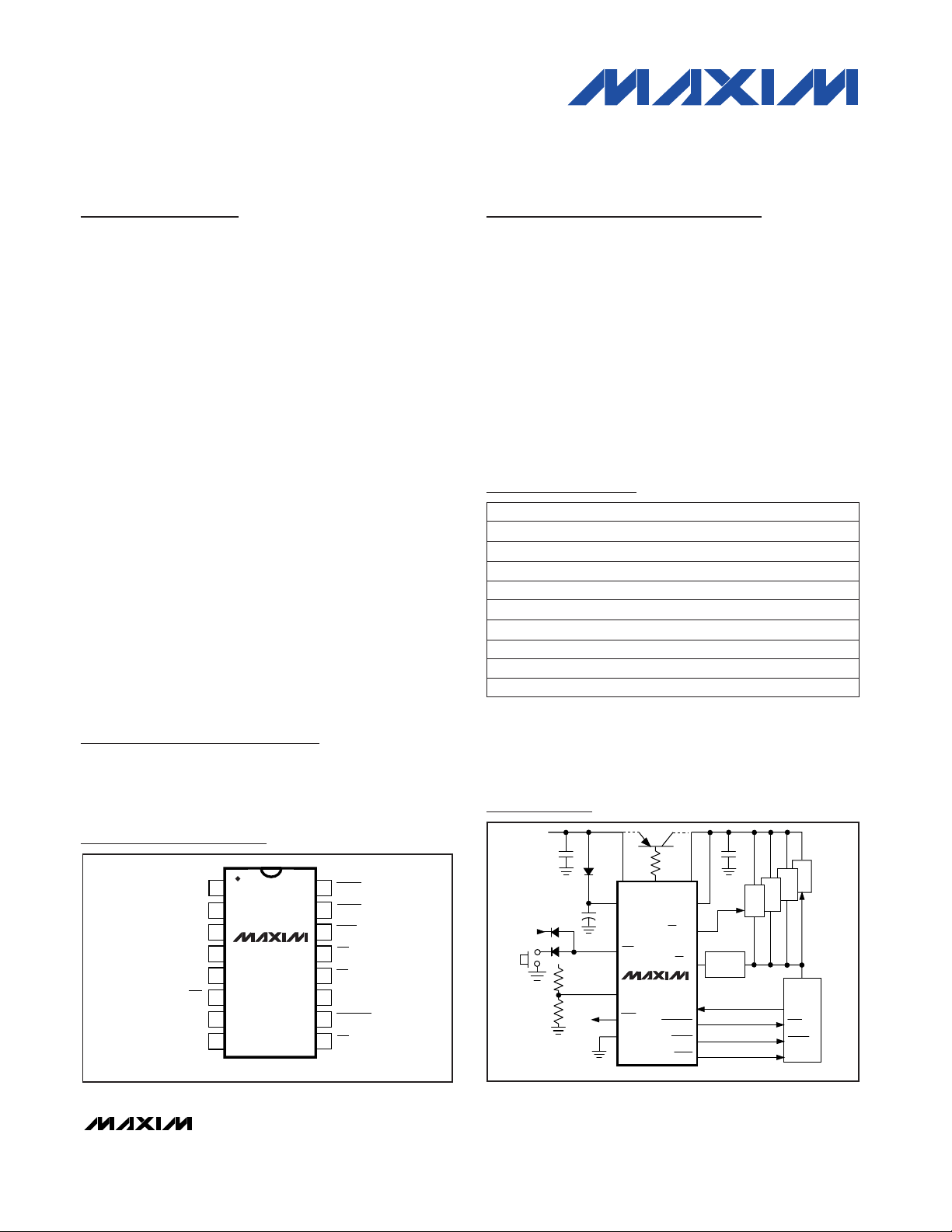
Ordering Information
16
15
14
13
12
11
10
9
1
2
3
4
5
6
7
8
WDPO
RESET
WDO
CE IN
GND
V
CC
V
OUT
VBATT
TOP VIEW
MAX791
CE OUT
WDI
LOWLINE
MR
SWT
PFI
PFO
BATT ON
DIP/SO/TSSOP
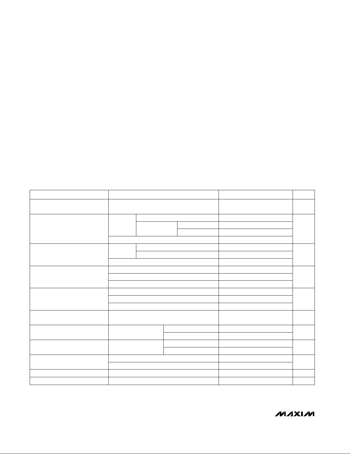
CMOS
RAM
MAX791
RESET
LOWLINE
WDI
CE IN
CE OUT
+5V
OTHER SYSTEM
RESET SOURCES
+12V
V
OUT
VBATT
*
MaxCap
A0–A15
MR
+12V SUPPLY
FAILURE
BATTONSWT
ADDRESS
DECODE
0.1µF
0.1µF
0.47F*
V
CC
PFI
PFO
GND
I/O
µP
NMI
INT
RESET
WDO
Pin Configuration
Typical Operating Circuit
PART TEMP RANGE PIN-PACKAGE
MAX791CPE 0°C to +70°C 16 Plastic DIP
MAX791CSE 0°C to +70°C 16 Narrow SO
MAX791C/D 0°C to +70°C Dice*
MAX791EPE -40°C to +85°C 16 Plastic DIP
MAX791ESE -40°C to +85°C 16 Narrow SO
MAX791EJE -40°C to +85°C 16 CERDIP
MAX791MJE -55°C to +125°C 16 CERDIP
MaxCap is a registered trademark of Cesiwid Inc. SuperCap is a registered trademark of Baknor Industries.
* Dice are specified at T
A
= +25°C.
Devices in PDIP, SO and TSSOP packages are available in both
leaded and lead-free packaging. Specify lead free by adding
the + symbol at the end of the part number when ordering.
Lead free not available for CERDIP package.
MAX791CUE 0°C to +70°C 16 TSSOP
MAX791EUE -40°C to +85°C 16 TSSOP
For pricing, delivery, and ordering information, please contact Maxim/Dallas Direct! at
1-888-629-4642, or visit Maxim’s website at www.maxim-ic.com.
Page 2
MAX791
Microprocessor Supervisory Circuit
2 _______________________________________________________________________________________
Input Voltage (with respect to GND)
VCC.......................................................................-0.3V to +6V
VBATT..................................................................-0.3V to + 6V
All Other Inputs.....................................-0.3V to (V
OUT
+ 0.3V)
Input Current
VCCPeak ..........................................................................1.0A
VCCContinuous ............................................................250mA
VBATT Peak ..................................................................250mA
VBATT Continuous ..........................................................25mA
GND, BATT ON .............................................................100mA
All Other Outputs ............................................................25mA
Continuous Power Dissipation (T
A
= +70°C)
Plastic DIP (derate 10.53mW/°C above +70°C) ..........842mW
Narrow SO (derate 8.70mW/°C above +70°C) ............696mW
CERDIP (derate 10.00mW/°C above +70°C)...............800mW
TSSOP (derate 6.70mW/°C above +70°C) ..................533mW
Operating Temperature Ranges
MAX791C_ _ ......................................................O°C to +70°C
MAX791E_ _ ....................................................-40°C to +85°C
MAX791MJE ..................................................-55°C to +125°C
Storage Temperature Range .............................-65°C to +160°C
Lead Temperature (soldering, 10s) .................................+300°C
ELECTRICAL CHARACTERISTICS
(VCC= 4.75V to 5.5V, VBATT = 2.8V, TA= T
MIN
to T
MAX
, unless otherwise noted.)
Stresses beyond those listed under “Absolute Maximum Ratings” may cause permanent damage to the device. These are stress ratings only, and functional
operation of the device at these or any other conditions beyond those indicated in the operational sections of the specifications is not implied. Exposure to
absolute maximum rating conditions for extended periods may affect device reliability.
ABSOLUTE MAXIMUM RATINGS
PARAMETER CONDITIONS
Supply Current in Battery-Backup
Mode (excludes I
OUT
) (Note 2)
MIN TYP MAX UNITS
VBATT = 4.5V, I
OUT
= 20mA VBATT - 0.3
Operating Voltage Range
VCC, VBATT (Note 1)
0 5.5 V
VCC- 0.3 VCC- 0.2
VCC- 0.05 VCC- 0.02
VBATT-to-V
OUT
On-Resistance
5
VBATT = 2.0V
µA
17 30
Ω
Battery-Switchover Threshold
Power down VBATT - 0.03
V
V
OUT
in Normal
Operating Mode
VCC= 3V, VBATT = 2.8V, I
OUT
= 100mA VCC- 0.2 VCC- 0.12
V
VCC= 4.5V
0.8 1.6
0.8 1.2
VCC= 4.5V
VCC- 0.40
VBATT = 2.8V, I
OUT
= 10mA VBATT - 0.25
0.04 1
Supply Current in Normal
Operating Mode (excludes I
OUT
)
VCC> VBATT - 1V 50 150 µA
VCC-to-V
OUT
On-Resistance
VCC= 3V 1.2 2.0
Ω
VBATT = 4.5V 815
VBATT = 2.8V
Power up
13 25
VBATT + 0.03
V
OUT
in Battery-Backup Mode
VBATT = 2.0V, I
OUT
= 5mA VBATT - 0.15
V
Battery-Switchover Hysteresis 60 mV
Low-Battery Detector Threshold 2 V
I
OUT
= 250mA
I
OUT
= 25mA
MAX791C/E
MAX791M
MAX791C/E
MAX791M
VCC< VBATT - 1.2V,
VBATT = 2.8V
TA= +25°C
TA= T
MIN
to T
MAX
VBATT Standby Current
(Note 3)
TA= T
MIN
to T
MAX
TA= +25°C
-1.0 0.02
µAVBATT + 0.2V ≤ V
CC
-0.1 0.02
Page 3
ns
MAX791
Microprocessor Supervisory Circuit
_______________________________________________________________________________________ 3
ELECTRICAL CHARACTERISTICS (continued)
(VCC= 4.75V to 5.5V, VBATT = 2.8V, TA= T
MIN
to T
MAX
, unless otherwise noted.)
0.7 1.5I
SINK
= 25mA
mA720Output source current
–W—D—P—O–
Output
Short-Circuit Current
V
0.1 0.4I
SINK
= 3.2mA
BATT ON Output
Low Voltage
ms104.7nF capacitor connected from SWT to GND
Minimum Watchdog
Timeout Period
ms1
–W—D—P—O–
Pulse Width
ns100VIL= 0.8V, VIH= 0.75 x V
CC
Minimum Watchdog Input
Pulse Width
µs80Power downVCC-to-–L—O—W
— —L—I—N—E–
Delay
s1.0 1.6 2.25SWT connected to V
OUT
V4.50 4.65 4.75
–R—E—S—E—T–
Threshold Voltage
mV150
–L—O—W— —L—I—N—E–
-to-–R—E—S—E—T
–
Threshold Voltage
µs100Power downVCC-to-–R—E—S—E—T–Delay
mV15
–R—E—S—E—T–
Threshold Hysteresis
Watchdog Timeout Period
ns70
–W—D—P—O–
-to-–W—D—O–Delay
µA
ms
115100Source current
BATT ON Output
Short-Circuit Current
mA60Sink current
140 200 280Power up
UNITSMIN TYP MAX
–R—E—S—E—T–
Active Timeout Period
CONDITIONSPARAMETER
0.004 0.3MAX791E/M, I
SINK
= 50µA, VCC= 1.2V, VCCfalling
0.1 0.4I
SINK
= 3.2mA, VCC= 4.25V
V
3.5I
SOURCE
= 1.6mA, VCC= 5V
–R—E—S—E—T–
Output Voltage
mA720Output source current
–R—E—S—E—T–
Output
Short-Circuit Current
0.4I
SINK
= 3.2mA, VCC= 4.25V
µA15 100Output source current
–L—O—W— —L—I—N—E–
Output
Short-Circuit Current
V
3.5I
SOURCE
= 1µA, VCC= 5V
–L—O—W— —L—I—N—E–
Output Voltage
0.4I
SINK
= 3.2mA
mA310Output source current
–W—D—O–
Output Short-Circuit Current
V
3.5I
SOURCE
= 500µA, VCC= 5V
–W—D—O–
Output Voltage
0.4I
SINK
= 3.2mA
V
3.5I
SOURCE
= 1mA
–W—D—P—O–
Output Voltage
0.004 0.3MAX791C, I
SINK
= 50µA, VCC= 1.0V, VCCfalling
RESET, LOW-LINE, AND WATCHDOG TIMER
Page 4
MAX791
Microprocessor Supervisory Circuit
4 _______________________________________________________________________________________
ELECTRICAL CHARACTERISTICS (continued)
(VCC= 4.75V to 5.5V, VBATT = 2.8V, TA= T
MIN
to T
MAX
, unless otherwise noted.)
Note 1: Either V
CC
or VBATT can go to 0V, if the other is greater than 2.0V.
Note 2: The supply current drawn by the MAX791 from the battery (excluding I
OUT
) typically goes to 10µA when
(VBATT - 1V) < V
CC
< VBATT. In most applications, this is a brief period as VCCfalls through this region.
Note 3: "+" = battery-discharging current, "-" = battery-charging current.
Note 4: WDI is internally connected to a voltage-divider between V
OUT
and GND. If unconnected, WDI is driven to 1.6V (typ),
disabling the watchdog function.
Note 5: The chip-enable resistance is tested with V
CC
= 4.75V V
–C—E–
IN
= V
C—E–OUT
= V
CC
/ 2.
Note 6: The chip-enable propagation delay is measured from the 50% point at –C—E–IN to the 50% point at –C—E–OUT.
ns
61050Ω source impedance driver, C
LOAD
= 50pF
–C—E–
IN-to-C—E–OUT Propagation
Delay (Note 6)
-50 -10WDI = 0V
µA
20 50WDI = V
OUT
WDI Input Current
0.75 x V
CC
V
IH
µA23 250
–M—R–
= 0V
–M—R–
Pull-Up Current
µs7
Ω75 150Enabled mode
–M—R–
-to -–R—E—S—E—T
–
Propagation Delay
–C—E–
IN-to-–C—E–OUT Resistance
(Note 5)
µA±0.005 ±1Disabled mode
–C—E–
IN Leakage Current
µs15Power down
–R—E—S—E—T–
-to-–C—E–OUT Delay
nA±0.01 ±25PFI Leakage Current
V1.25VCC= 5V
–M—R–
Threshold
mA0.1 0.75 2.0
µs
Disabled mode, –C—E–OUT = 0V
25 15
–C—E–
OUT Short-Circuit Current
(Reset Active)
V1.20 1.25 1.30VCC= 5VPFI Input Threshold
V
0.8V
IL
WDI Threshold Voltage
(Note 4)
UNITSMIN TYP MAX
–M—R–
Minimum Pulse Width
CONDITIONSPARAMETER
0.4I
SINK
= 3.2mA
V
3.5I
SOURCE
= 1µA, VCC= 5V
–P—F—O–
Output Voltage
mA60Output sink current
µA115100Output source current
–P—F—O–
Short-Circuit Current
µs
55VIN= 20mV, VOD= 15mV
PFI-to-–P—F—O–Delay
15VIN= -20mV, VOD= 15mV
3.5VCC= 5V, I
OUT
= -100µA
V
2.7VCC= 0V, VBATT = 2.8V, I
OUT
= 1µA
–C—E–
OUT Output Voltage High
(Reset Active)
POWER-FAIL COMPARATOR
CHIP-ENABLE GATING
MANUAL RESET INPUT
Page 5
MAX791
Microprocessor Supervisory Circuit
58
38
-60 -30 30 150
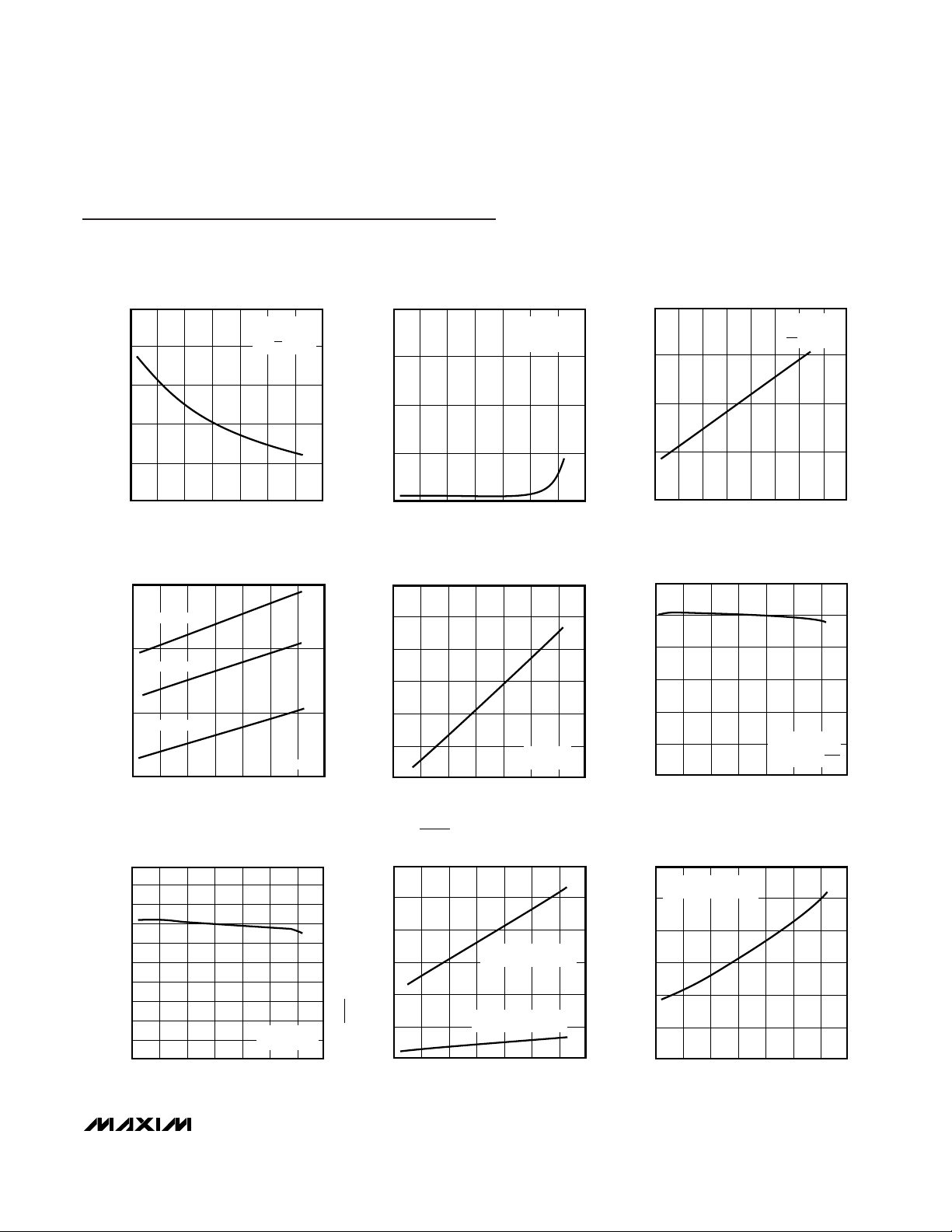
VCC SUPPLY CURRENT vs. TEMPERATURE
(NORMAL OPERATING MODE)
42
54
MAX791-01
TEMPERATURE (°C)
V
CC
SUPPLY CURRENT (µA)
0 1209060
46
50
VCC = +5V
VBATT = 2.8V
PFI, CE IN = 0V
4.80
4.30
4.40
4.35
-60 -30 30 150
RESET THRESHOLD
vs. TEMPERATURE
MAX791-07
TEMPERATURE (°C)
RESET THRESHOLD (V)
0 1209060
4.45
4.50
4.55
4.60
4.65
4.70
4.75
VBATT = 0V,
POWER DOWN
600
0
100
-60 -30 30 150
RESET OUTPUT RESISTANCE
vs. TEMPERATURE
MAX791-08
TEMPERATURE (°C)
RESET OUTPUT RESISTANCE (Ω)
0 1209060
200
300
400
500
VCC = 0V, VBATT = 2.8V
SINKING CURRENT
VCC = +5V, VBATT = 2.8V
SOURCING CURRENT
230
170
180
-60 -30 30 150
RESET DELAY
vs. TEMPERATURE
MAX791-09
TEMPERATURE (°C)
RESET DELAY (ms)
01209060
190
200
210
220
VCC = 0V TO 5V STEP
VBATT = 2.8V
Typical Operating Characteristics
(TA = +25°C, unless otherwise noted.)
20
5
-60 -30 30 150
VBATT-to-V
OUT
ON-RESISTANCE
vs. TEMPERATURE
MAX791-04
TEMPERATURE (°C)
VBATT-to-V
OUT
ON-RESISTANCE (Ω)
0 1209060
10
15
VBATT = 2.0V
VBATT = 2.8V
VBATT = 4.5V
VCC = 0V
2.0
0
-60 -30 30 150
BATTERY-SUPPLY CURRENT vs. TEMPERATURE
(BATTERY-BACKUP MODE)
0.5
MAX791-02
TEMPERATURE (°C)
BATTERY SUPPLY CURRENT (µA)
0 1209060
1.0
1.5
VCC = 0V
VBATT = 2.8V
NO LOAD
120
40
-60 -30 30 150 180
CHIP-ENABLE ON-RESISTANCE
vs. TEMPERATURE
60
MAX791-03
TEMPERATURE (°C)
CE ON-RESISTANCE (Ω)
0 1209060
80
100
VCC = +4.75V
VBATT = 2.8V
CE IN = V
CC
/2
1.2
0.6
0.7
-60 -30 30 150
VCC-to-V
OUT
ON-RESISTANCE
vs. TEMPERATURE
MAX791-05
TEMPERATURE (°C)
V
CC
-to-V
OUT
ON-RESISTANCE (
Ω
)
0 1209060
0.8
0.9
1.0
1.1
VCC = +5V,
VBATT = 0V
1.50
0
0.25
-60 -30 30 150
PFI THRESHOLD
vs. TEMPERATURE
MAX791-05
TEMPERATURE (°C)
PFI THRESHOLD (V)
01209060
0.50
0.75
1.00
1.25
VCC = +5V,
VBATT = 0V,
NO LOAD ON PFO
_______________________________________________________________________________________ 5
Page 6
MAX791
Microprocessor Supervisory Circuit
6 _______________________________________________________________________________________
Typical Operating Characteristics (continued)
(TA = +25°C, unless otherwise noted.)
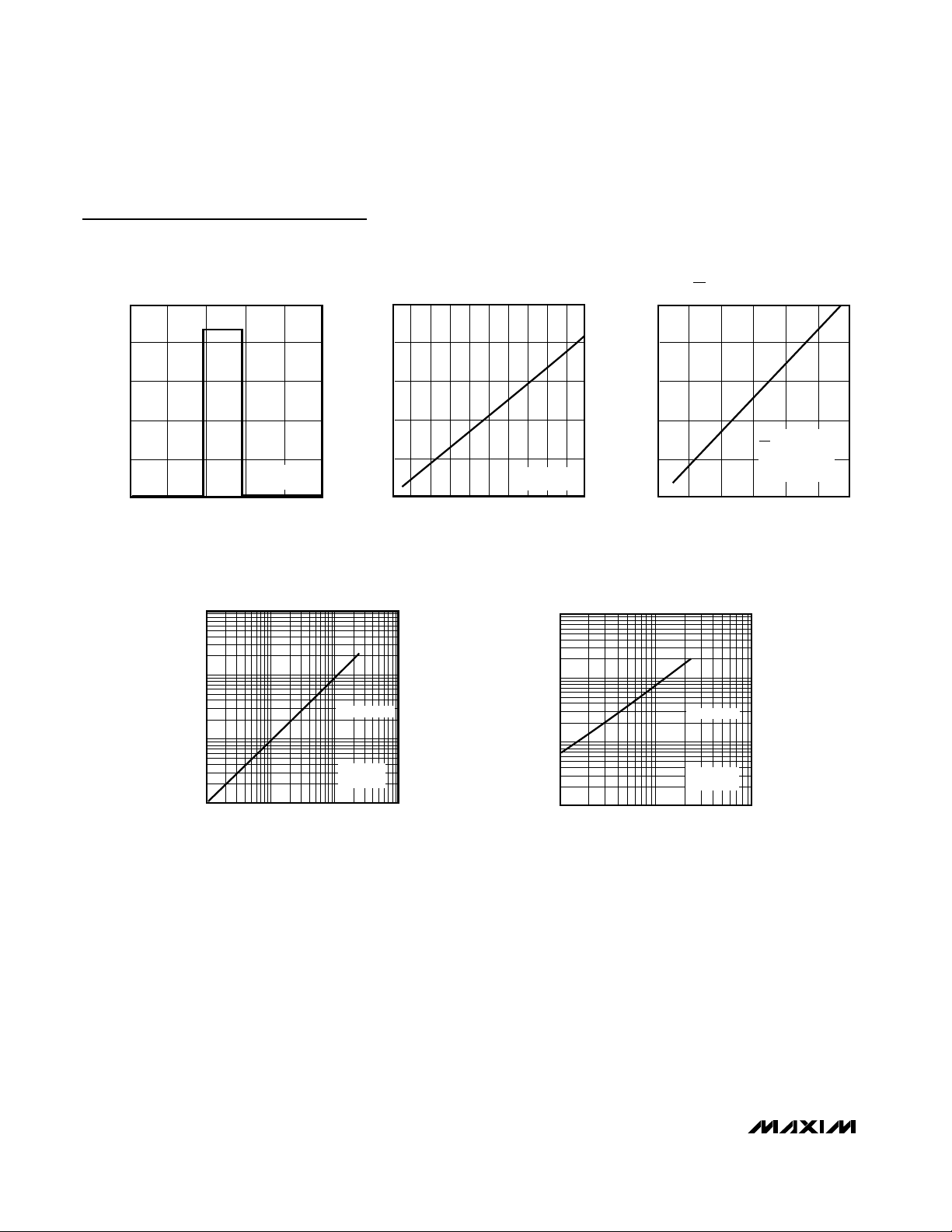
1000
1
1 100 1000
VCC to V
OUT
vs.
OUTPUT CURRENT
10
100
MAX791-13
I
OUT
(mA)
V
CC
- V
OUT
(mV)
10
VCC = 4.5V
VBATT = 0V
SLOPE = 0.8Ω
1000
1
110100
VBATT to V
OUT
vs.
OUTPUT CURRENT
MAX791-14
I
OUT
(mA)
VBATT - V
OUT
(mV)
10
100
VCC = 0V
VBATT = 4.5V
SLOPE = 8Ω
0
50
04020
WATCHDOG TIMEOUT
vs. TIMING CAPACITOR
MAX791-11
TIMING CAPACITOR (nF)
WATCHDOG TIMEOUT (ms)
3010 70 80 90 1006050
100
150
200
250
VCC = +5V
VBATT = 2.8V
0
4
0 10050
CHIP-ENABLE PROPAGATION DELAY
vs. CE OUT LOAD CAPACITANCE
MAX791-12
C
LOAD
(pF)
PROPAGATION DELAY (ns)
200 250 300150
8
12
16
20
VCC = +5V
CE IN = 0V TO 5V
DRIVER SOURCE
IMPEDANCE = 50Ω
0
4
8
15
BATTERY CURRENT
vs. INPUT SUPPLY VOLTAGE
MAX791-10
VCC (V)
I
BATT
(µA)
0432
12
16
20
VBATT = 2.8V,
I
OUT
= 0A
Page 7

MAX791
Microprocessor Supervisory Circuit
_______________________________________________________________________________________ 7
Pin Description
PIN NAME FUNCTION
1 VBATT
2V
OUT
Output Supply Voltage. V
OUT
connects to VCCwhen VCCis greater than VBATT and VCCis above the reset
threshold. When VCCfalls below VBATT and VCCis below the reset threshold, V
OUT
connects to VBATT.
Connect a 0.1µF capacitor from V
OUT
to GND.
3V
CC
Input Supply Voltage—+5V input
4 GND
5 BATT ON
6
–P—F—O–
7 PFI
8 SWT
9
–M—R–
10–L—O—W
— —L—I—N—E–
11 WDI
12–C—E–OUT
Chip-Enable Output. –C—E– OUT goes low only when ––C—E–IN is low and V
CC
is above the reset threshold. If –C—E–IN is
low when reset is asserted, –C—E–OUT will stay low for 15µs or until –C—E–IN goes high, whichever occurs first.
13––C—E–IN
Backup-Battery Input. Connect to external battery or capacitor and charging circuit.
Ground. 0V reference for all signals.
Battery-On Output. Goes high when V
OUT
switches to VBATT. Goes low when V
OUT
switches to VCC. Connect
the base of a PNP through a current-limiting resistor to BATT ON for V
OUT
current requirements greater than
250mA.
Power-Fail Output. This is the output of the power-fail comparator. –P—F—O–goes low when PFI is less than 1.25V.
This is an uncommitted comparator, and has no effect on any other internal circuitry.
Power-Fail Input. This is the noninverting input to the power-fail comparator. When PFI is less than 1.25V,
–P—F—O–
goes low. Connect PFI to GND or V
OUT
when not used.
Set Watchdog-Timeout Input. Connect this input to V
OUT
to select the default 1.6s watchdog-timeout period.
Connect a capacitor between this input and GND to select another watchdog-timeout period. Watchdog-timeout
period = 2.1 x (capacitor value in nF) ms.
16–W—D—P—O
–
15–R—E—S—E—T
–
14–W—D—O
–
Manual-Reset Input. This input can be tied to an external momentary pushbutton switch, or to a logic gate output. –R—E—S—E—T–remains low as long as–M—R–is held low and for 200ms after–M—R–returns high.
–L—O—W— —L—I—N—E–
Output goes low when V
CC
falls to 150mV above the reset threshold. The output can be used to gen-
erate an NMI if the unregulated supply is inaccessible.
Watchdog Input. WDI is a three-level input. If WDI remains either high or low for longer than the watchdog timeout period, –W—D—O–goes low. –W—D—O–remains low until the next transition at WDI. Leaving WDI unconnected disables
the watchdog function. WDI connects to an internal voltage-divider between V
OUT
and GND, which sets it to mid-
supply when left unconnected.
Chip-Enable Input. The input to chip-enable gating circuit. Connect to GND or V
OUT
if not used.
Watchdog Output. –W—D—O–goes low if WDI remains either high or low longer than the watchdog-timeout period.
–W—D—O–
returns high on the next transition at WDI. –W—D—O–remains high if WDI is unconnected. –W—D—O–is also high
when –R—E—S—E—T–is asserted.
–R—E—S—E—T–
Output goes low whenever V
CC
falls below the reset threshold. –R—E—S—E—T–will remain low for typically 200ms
after VCCcrosses the reset threshold on power-up.
Watchdog-Pulse Output. Upon the absence of a transition at WDI, –W—D—P—O–will pulse low for a minimum of 1ms.
–W—D—P—O–
precedes ––W—D—O– by 70ns.
Page 8

_______________Detailed Description
Manual Reset Input
Many µP-based products require manual-reset capability, allowing the operator or test technician to initiate a
reset. The Manual Reset Input (MR) can be connected
directly to a switch, without an external pull-up resistor
or debouncing network. It connects to a 1.25V comparator, and has a pull-up to V
OUT
as shown in Figure
1. The propagation delay from asserting MR to RESET
asserted is 4µs typ. Pulsing MR low for a minimum of
15µs resets all the internal counters, sets the Watchdog
Output (WDO) and Watchdog-Pulse Output (WDPO)
high, and sets the Set Watchdog-Timeout (SWT) input
to V
OUT
- 0.6V, if it is not already connected to V
OUT
(for internal timeouts). It also disables the chip-enable
function, setting the Chip-Enable Output (CE OUT) to a
high state. The RESET output remains active as long as
MR is held low, and the reset-timeout period begins
after MR returns high (Figure 2).
Use this input as either a digital-logic input or a second
low-line comparator. Normal TTL/CMOS levels can be
wire-OR connected via pull-down diodes (Figure 3),
and open-drain/collector outputs can be wire-ORed
directly.
MAX791
Microprocessor Supervisory Circuit
8 _______________________________________________________________________________________
MAX791
CHIP-ENABLE
OUTPUT
CONTROL
V
CC
3
1
13
9
8
11
7
VBATT
CE IN
MR
SWT
WDI
PFI
RESET
GENERATION
TIMEBASE FOR
RESET AND
WATCHDOG
WATCHDOG
TRANSITION
DETECTOR
WATCHDOG
TIMER
V
OUT
1.25V
GND
4
4.65V
150mV
10
LOWLINE
5
2
12
15
16
14
PFO
WDO
WDPO
RESET
CE OUT
6
V
OUT
BATT ON
Figure 1. MAX791 Block Diagram
MR
RESET
CE IN
0V
7.5µs TYP
15µs TYP
25µs MIN
CE OUT
Figure 2. Manual-Reset Timing Diagram
MAX791
*
*
OTHER
RESET
SOURCES
MANUAL RESET
MR
* DIODES NOT REQUIRED ON OPEN-DRAIN OUTPUTS
Figure 3. Diode "OR" Connections Allow Multiple Reset Sources
to Connect to MR
Page 9

RESET Output
The MAX791’s RESET output ensures that the µP powers up in a known state, and prevents code-execution
errors during power-down or brownout conditions.
The RESET output is active low, and typically sinks
3.2mA at 0.1V saturation voltage in its active state.
When deasserted, RESET sources 1.6mA at typically
V
OUT
- 0.5V. When no backup battery is used, RESET
output is guaranteed to be valid down to VCC= 1V, and
an external 10kΩ pull-down resistor on RESET ensures
that RESET will be valid with VCCdown to GND (Figure
4). As VCCgoes below 1V, the gate drive to the RESET
output switch reduces accordingly, increasing the
r
DS(ON)
and the saturation voltage. The 10kΩ pull-down
resistor ensures the parallel combination of switch plus
resistor is around 10kΩ and the output saturation voltage is below 0.4V while sinking 40µA. When using a
10kΩ external pull-down resistor, the high state for the
RESET output with VCC= 4.75V is 4.5V typ. For battery
voltages ≥ 2V connected to VBATT, RESET remains
valid for V
CC
from 0V to 5.5V.
RESET will be asserted during the following conditions:
•VCC< 4.65V (typ).
•MR< 1.25V (typ).
• RESET remains asserted for 200ms (typ) after V
CC
rises above 4.65V or after MR has exceeded
1.25V.
The MAX791 battery-switchover comparator does not
affect RESET assertion. However, RESET is asserted in
battery-backup mode since V
CC
must be below the
reset threshold to enter this mode.
Watchdog Function
The watchdog monitors µP activity via the Watchdog
Input (WDI). If the µP becomes inactive, WDO and
WDPO are asserted. To use the watchdog function,
connect WDI to a bus line or µP I/O line. If WDI remains
high or low for longer than the watchdog timeout period
(1.6s nominal), WDPO and WDO are asserted, indicating a software fault condition (see Watchdog Output
and Watchdog-Pulse Output sections).
Watchdog Input
A change of state (high to low, low to high, or a minimum 100ns pulse) at WDI during the watchdog period
resets the watchdog timer. The watchdog default timeout is 1.6s. Select alternative timeout periods by connecting an external capacitor from SWT to GND (see
Selecting an Alternative Watchdog Timeout Period section).
To disable the watchdog function, leave WDI floating.
An internal resistor network (100kΩ equivalent impedance at WDI) biases WDI to approximately 1.6V.
Internal comparators detect this level and disable the
watchdog timer. When V
CC
is below the reset threshold, the watchdog function is disabled and WDI is disconnected from its internal resistor network, thus
becoming high impedance.
Watchdog Output
WDO remains high if there is a transition or pulse at
WDI during the watchdog-timeout period. The watchdog function is disabled and WDO is a logic high when
VCCis below the reset threshold, battery-backup mode
is enabled, or WDI is an open circuit. In watchdog
mode, if no transition occurs at WDI during the watchdog-timeout period, WDO goes low 70ns after the
falling edge of WDPO and remains low until the next
transition at WDI (Figure 5). A flip-flop can force the
system into a hardware shutdown if there are two successive watchdog faults (Figure 6). WDO has a 2 x TTL
output characteristic.
MAX791
Microprocessor Supervisory Circuit
_______________________________________________________________________________________ 9
MAX791
RESET
10k
TO µP RESET
15
Figure 4. Adding an External Pull-Down Resistor Ensures
–R—E—S—E—T–
is Valid with VCCDown to GND
WDPO
WDI
70ns
1.6s
100ns MIN
WDO
Figure 5. WDI, –W—D—O–, and –W—D—P—O–Timing Diagram (VCCMode)
Page 10

MAX791
Watchdog-Pulse Output
As described in the preceding section, WDPO can be
used as the clock input to an external D flip-flop. Upon
the absence of a watchdog edge or pulse at WDI at the
end of a watchdog-timeout period, WDPO will pulse low
for 1ms. The falling edge of WDPO precedes WDO by
70ns. Since WDO is high when WDPO goes low, the
flip-flop’s Q output remains high as WDO goes low
(Figure 5). If the watchdog timer is not reset by a transition at WDI, WDO remains low and WDPO clocks a
logic low to the Q output, causing the MAX791 to latch
in reset. If the watchdog timer is reset by a transition at
WDI, WDO goes high and the flip-flop’s Q output
remains high. Thus, a system shutdown is only caused
by two successive watchdog faults.
The internal pull-up resistors associated with WDO and
WDPO connect to V
OUT
. Therefore, do not connect
these outputs directly to CMOS logic that is powered
from VCCsince, in the absence of VCC(i.e., battery
mode), excessive current will flow from WDO or
WDPO through the protection diode(s) of the CMOSlogic inputs to ground.
Selecting an Alternative Watchdog-
Timeout Period
SWT input controls the watchdog-timeout period.
Connecting SWT to V
OUT
selects the internal 1.6s watch-
dog-timeout period. Select an alternative timeout period
by connecting a capacitor between SWT and GND. Do
not leave SWT floating, and do not connect it to ground.
The following formula determines the watchdog-timeout
period:
Watchdog-timeout period = 2.1 x (capacitor value
in nF) ms
This formula is valid for capacitance values between
4.7nF and 100nF (see the Watchdog Timeout vs.
Timing Capacitor graph in the Typical Operating
Characteristics). SWT is internally connected to a
±100nA (typ) current source, which charges and discharges the timing capacitor to create the oscillator frequency that sets the watchdog-timeout period (see
Connecting a Timing Capacitor to SWT section).
Chip-Enable Signal Gating
The MAX791 provides internal gating of chip-enable
(CE) signals to prevent erroneous data from corrupting
the CMOS RAM in the event of a power failure. During
normal operation, the CE gate is enabled and passes
all CE transitions. When reset is asserted, this path
becomes disabled, preventing erroneous data from
corrupting the CMOS RAM. The MAX791 uses a series
transmission gate from the Chip-Enable Input (CE IN) to
CE OUT (Figure 1).
The 10ns max CE propagation from CE IN to CE OUT
Microprocessor Supervisory Circuit
10 ______________________________________________________________________________________
MAX791
CLOCK
V
CC
CD4013
V
CC
GND
V
OUT
MR
0.1µF
4.7k
*SETS Q HIGH ON POWER-UP
VBATT
RESET
WDI
WDPO
WDO
µP POWER
µP
RESET
TWO
CONSECUTIVE
WATCHDOG
FAULT
INDICATIONS
I/O
Q
D
Q
SET RESET V
SS
2
15
11
LOWLINE
NMI
INTERRUPT
10
16
1/6 74HC04
14
1
5
3
14
3
2
7
46
*1µF
+5V
1
9
4
REACTIVATE
+5V
3.6V
Figure 6. Two Consecutive Watchdog Faults Latch the System in Reset
Page 11

enables the MAX791 to be used with most µPs.
Chip-Enable Input
CE IN is high impedance (disabled mode) while RESET
is asserted.
During a power-down sequence where VCCpasses
4.65V, CE IN assumes a high-impedance state when
the voltage at CE IN goes high or 15µs after reset is
asserted, whichever occurs first (Figure 7).
During a power-up sequence, CE IN remains high
impedance, regardless of CE IN activity, until reset is
deasserted following the reset-timeout period.
In the high-impedance mode, the leakage currents into
this input are ±1µA max over temperature. In the lowimpedance mode, the impedance of CE IN appears as
a 75Ω resistor in series with the load at CE OUT.
The propagation delay through the CE transmission
gate depends on both the source impedance of the
drive to CE IN and the capacitive loading on CE OUT
(see the Chip-Enable Propagation Delay vs. CE OUT
Load Capacitance graph in the Typical Operating
Characteristics). The CE propagation delay is production tested from the 50% point on CE IN to the 50%
point on CE OUT using a 50Ω driver and 50pF of load
capacitance (Figure 8). For minimum propagation
delay, minimize the capacitive load at CE OUT and use
a low output-impedance driver.
Chip-Enable Output
In the enabled mode, the impedance of CE OUT is
equivalent to 75Ω in series with the source driving CE
IN. In the disabled mode, the 75Ω transmission gate is
off and CE OUT is actively pulled to V
OUT
. This source
turns off when the transmission gate is enabled.
LOWLINE Output
The low-line comparator monitors VCCwith a typical
threshold voltage 150mV above the reset threshold,
and has 15mV of hysteresis. LOWLINE typically sinks
3.2mA at 0.1V. For normal operation (VCCabove the
LOWLINE threshold), LOWLINE is pulled to V
OUT
. If
access to the unregulated supply is unavailable, use
LOWLINE to provide a nonmaskable interrupt (NMI) to
the µP as VCCbegins to fall (Figure 9a).
Power-Fail Comparator
The power-fail comparator is an uncommitted comparator that has no effect on the other functions of the IC.
Common uses include monitoring supplies other than
5V (see the Typical Operating Circuit and the
Monitoring a Negative Voltage section) and early
power-fail detection when the unregulated power is
easily accessible (Figure 9b).
MAX791
Microprocessor Supervisory Circuit
______________________________________________________________________________________ 11
V
CC
CE IN
RESET
THRESHOLD
CE OUT
RESET
RESET
100µs
15µs
100µs
Figure 7. Reset and Chip-Enable Timing
MAX791
CE IN
C
LOAD
CE OUT
GND
+5V
50Ω DRIVER
V
CC
Figure 8. CE Propagation Delay Test Circuit
Page 12

MAX791
Power-Fail Input
PFI is the input to the power-fail comparator. PFI has a
guaranteed input leakage of ±25nA max over temperature. The typical comparator delay is 15µs from VILto
VOL(power failing), and 55µs from VIHto VOH(power
being restored). If unused, connect this input to
ground.
Power-Fail Output
The Power-Fail Output (PFO) goes low when PFI goes
below 1.25V. It typically sinks 3.2mA with a saturation
voltage of 0.1V. With PFI above 1.25V, PFO is actively
pulled to V
OUT
. Connecting PFI through a voltagedivider to an unregulated supply allows PFO to generate an NMI as the unregulated power begins to fall
(Figure 9b). If the unregulated supply is inaccessible,
use LOWLINE to generate the NMI. The LOWLINE
threshold is typically 150mV above the reset threshold
(see LOWLINE Output section).
Battery-Backup Mode
The MAX791 requires two conditions to switch to battery-backup mode: 1) V
CC
must be below the reset
threshold; 2) V
CC
must be below VBATT. Table 1 lists
the status of the inputs and outputs in battery-backup
mode.
Microprocessor Supervisory Circuit
12 ______________________________________________________________________________________
Table 1. Input and Output States in
Battery-Backup Mode
* VCCmust be below the reset threshold to enter batterybackup mode.
Logic high. The open-circuit output
voltage is equal to V
OUT
.
–W—D—P—O–
16
Logic low*
–R—E—S—E—T–
15
Logic high. The open-circuit output
voltage is equal to V
OUT
.
–W—D—O–
14
High impedance
–C—E–
IN
13
Logic high. The open-circuit output
voltage is equal to V
OUT
.
–C—E–
OUT
12
WDI is ignored, and goes high
impedance.
WDI11
Logic low*
–L—O—W—L—I—N—E–
10
––M—R–
is ignored.
–M—R–
9
SWT is ignored.SWT8
The power-fail comparator remains
active in the battery-backup mode for
VCC≥ VBATT - 1.2V typ.
PFI7
The power-fail comparator remains
active in the battery-backup mode for
VCC≥ VBATT - 1.2V typ. Below this
voltage, –P—F—O–is forced low.
–P—F—O–
6
Logic high. The open-circuit output is
equal to V
OUT
.
BATT ON5
GND—0V reference for all signals.GND4
Battery-switchover comparator
monitors VCCfor active switchover.
V
CC
3
V
OUT
is connected to VBATT through
an internal PMOS switch.
V
OUT
2
Supply current is 1µA maximum.VBATT1
STATUSNAMEPIN
Figure 9. a) If the unregulated supply is inaccessible,
LOWLINE generates the NMI for the µP. b) Use PFO to generate the µP NMI if the unregulated supply is inaccessible.
FROM
REGULATED
SUPPLY
0.1µF
3
V
CC
MAX791
V
OUT
VBATT
2
0.1µF
1
3.0V
µP POWER
POWER TO
CMOS RAM
µP
15
RESET
10
LOWLINE
11
WDI
GND
a)
VOLTAGE
REGULATOR
4
3
V
CC
0.1
µF
MAX791
7
PFI
GND
4
V
OUT
VBATT
RESET
PFO
WDI
2
1
15
6
11
b)
RESET
NMI
I/O LINE
POWER TO
CMOS RAM
0.1µF
3.0V
RESET
NMI
I/O LINE
µP POWER
µP
Page 13

Battery On Output
The Battery On (BATT ON) output indicates the status
of the internal VCC/battery-switchover comparator,
which controls the internal VCCand VBATT switches.
For VCCgreater than VBATT (ignoring the small hysteresis effect), BATT ON typically sinks 3.2mA at 0.1V
saturation voltage. In battery-backup mode, this terminal sources approximately 10µA from V
OUT
. Use BATT
ON to indicate battery-switchover status or to supply
base drive to an external pass transistor for higher-current applications (see Typical Operating Circuit).
Input Supply Voltage
The Input Supply Voltage (VCC) should be a regulated
+5V. V
CC
connects to V
OUT
via a parallel diode and a
large PMOS switch. The switch carries the entire current load for currents less than 250mA. The parallel
diode carries any current in excess of 250mA. Both the
switch and the diode have impedances less than 1Ω
each (Figure 10). The maximum continuous current is
250mA, but power-on transients may reach a maximum
of 1A.
Backup-Battery Input
The Backup-Battery Input (VBATT) is similar to VCC,
except the PMOS switch and parallel diode are much
smaller. Accordingly, the on-resistances of the diode
and the switch are each approximately 10Ω.
Continuous current should be limited to 25mA and peak
currents (only during power-up) limited to 250mA. The
reverse leakage of this input is less than 1µA over temperature and supply voltage.
Output Supply Voltage
The Output Supply Voltage (V
OUT
) is internally connected to the substrate of the IC and supplies all the current
to the external system and internal circuitry. All opencircuit outputs will, for example, assume the V
OUT
volt-
age in their high states rather than the V
CC
voltage. At
the maximum source current of 250mA, V
OUT
will typically be 200mV below VCC. Decouple this terminal with
a 0.1µF capacitor.
Low-Battery Monitor
The MAX791 low-battery voltage function monitors
VBATT. Low-battery detection of 2.0V ±0.15V is monitored only during the reset-timeout period (200ms) that
occurs either after a normal power-up sequence or
after the MR reset input has been returned to its high
state. If the battery voltage is below 2.0V, the second
CE pulse is inhibited after reset timeout. If the battery
voltage is above 2.0V, all CE pulses are allowed
through the CE gate after the reset timeout period. To
use this function, after the 200ms reset delay, write 00
(HEX) to a location using the first CE pulse, and write
FF (HEX) to the same location using the second CE
pulse following RESET going inactive on power-up. The
contents of the memory then indicates a good battery
(FF) or a low battery (00) (Figure 11).
MAX791
Microprocessor Supervisory Circuit
______________________________________________________________________________________ 13
200ms TYP
RESET
THRESHOLD
V
CC
RESET
CE IN
CE OUT
SECOND CE PULSE ABSENT WHEN VBATT < 2V
Figure 11. Backup-Battery Monitor Timing Diagram
MAX791
VBATT
V
CC
1
3
2
0.1µF
V
OUT
Figure 10. VCCand VBATT-to-V
OUT
Switch
Page 14

MAX791
Applications Information
The MAX791 is not short-circuit protected. Shorting
V
OUT
to ground, other than power-up transients such
as charging a decoupling capacitor, destroys the
device.
All open-circuit outputs swing between V
OUT
and GND
rather than VCCand GND.
If long leads connect to the chip inputs, ensure that
these lines are free from ringing and other conditions
that would forward bias the chip’s protection diodes.
There are three distinct modes of operation:
1) Normal operating mode with all circuitry powered
up. Typical supply current from VCCis 60µA, while
only leakage currents flow from the battery.
2) Battery-backup mode where VCCis typically within
0.7V below VBATT. All circuitry is powered up and
the supply current from the battery is typically less
than 60µA.
3) Battery-backup mode where VCCis less than
VBATT by at least 0.7V. VBATT supply current is
less than 1µA max.
Using SuperCaps or MaxCaps
with the MAX791
VBATT has the same operating voltage range as VCC,
and the battery-switchover threshold voltages are typi-
cally ±30mV centered at VBATT, allowing use of a
SuperCap and a simple charging circuit as a backup
source (Figure 12).
If V
CC
is above the reset threshold and VBATT is 0.5V
above VCC, current flows to V
OUT
and VCCfrom VBATT
until the voltage at VBATT is less than 0.5V above VCC.
For example, with a SuperCap connected to VBATT
and through a diode to VCC, if VCCquickly changes
from 5.4V to 4.9V, the capacitor discharges through
V
OUT
and VCCuntil VBATT reaches 5.3V typ. Leakage
current through the SuperCap charging diode and
MAX791 internal power diode eventually discharges the
SuperCap to VCC. Also, if VCCand VBATT start from
0.5V above the reset threshold and power is lost at
VCC, the SuperCap on VBATT discharges through V
CC
until VBATT reaches the reset threshold; the MAX791
then switches to battery-backup mode and the current
through V
CC
goes to zero (Figure 10).
Using Separate Power Supplies
for VBATT and V
CC
If using separate power supplies for VCCand VBATT,
VBATT must be less than 0.3V above VCCwhen VCCis
above the reset threshold. As described in the previous
section, if VBATT exceeds this limit and power is lost at
VCC, current flows continuously from VBATT to VCCvia
the VBATT-to-V
OUT
diode and the V
OUT
-to-VCCswitch
until the circuit is broken (Figure 10).
Alternative Chip-Enable Gating
Using memory devices with CE and CE inputs allows
the MAX791 CE loop to be bypassed. To do this, connect CE IN to ground, pull up CE OUT to V
OUT
, and
connect CE OUT to the CE input of each memory
device (Figure 13). The CE input of each part then connects directly to the chip-select logic, which does not
have to be gated by the MAX791.
Adding Hysteresis to the
Power-Fail Comparator
Hysteresis adds a noise margin to the power-fail comparator and prevents repeated triggering of PFO when
VIN is near the power-fail comparator trip point. Figure
14 shows how to add hysteresis to the power-fail comparator. Select the ratio of R1 and R2 so that PFI sees
1.25V when VIN falls to the desired trip point (V
TRIP
).
Resistor R3 adds hysteresis. It will typically be an order
of magnitude greater than R1 or R2. The current
through R1 and R2 should be at least 1µA to ensure
that the 25nA (max) PFI input current does not shift the
trip point. R3 should be larger than 10kΩ to prevent it
from loading down the PFO pin. Capacitor C1 adds
additional noise rejection.
Microprocessor Supervisory Circuit
14 ______________________________________________________________________________________
MAX791
1
0.47F
1N4148
+5V
2
3
V
CC
GND
VBATT
4
V
OUT
Figure 12. SuperCap or MaxCap on VBATT
Page 15

Monitoring a Negative Voltage
The power-fail comparator can be used to monitor a
negative supply voltage using Figure 15’s circuit. When
the negative supply is valid, PFO is low. When the negative supply voltage drops, PFO goes high. This circuit’s accuracy is affected by the PFI threshold tolerance, the VCCvoltage, and resistors R1 and R2.
Backup-Battery Replacement
The backup battery may be disconnected while VCCis
above the reset threshold. No precautions are necessary to avoid spurious reset pulses.
Negative-Going VCCTransients
While issuing resets to the µP during power-up, powerdown, and brownout conditions, these supervisors are
relatively immune to short-duration negative-going V
CC
transients (glitches). It is usually undesirable to reset
the µP when VCCexperiences only small glitches.
Figure 16 shows maximum transient duration vs. reset
comparator overdrive, for which reset pulses are not
generated. The graph was produced using negative-
going VCCpulses, starting at 5V and ending below the
reset threshold by the magnitude indicated (reset comparator overdrive). The graph shows the maximum
pulse width that a negative-going VCCtransient may
typically have without causing a reset pulse to be
issued. As the amplitude of the transient increases (i.e.,
goes farther below the reset threshold), the maximum
allowable pulse width decreases. Typically, a VCCtransient that goes 100mV below the reset threshold and
lasts for 40µs or less will not cause a reset pulse to be
issued.
A 100nF bypass capacitor mounted close to the V
CC
pin provides additional transient immunity.
Connecting a Timing Capacitor to SWT
SWT is internally connected to a ±100nA current
source. When a capacitor is connected from SWT to
ground (to select an alternative watchdog-timeout period), the current source charges and discharges the
timing capacitor to create the oscillator that controls the
watchdog-timeout period. To prevent timing errors or
oscillator start-up problems, minimize external current
leakage sources at this pin, and locate the capacitor as
MAX791
Microprocessor Supervisory Circuit
______________________________________________________________________________________ 15
MAX791
V
CC
GND
PFI
*OPTIONAL
R2
R3
R1
V
IN
+5V
C1*
TO µP
PFO
V
TRIP
= 1.25
R1 + R2
R2
V
H
= 1.25 /
R2
|| R3
VL - 1.25 + 5 - 1.25 = 1.25
R1 + R2
||
R3 R1 R3 R2
PFO
+5V
0V
0V V
H
V
TRIP
V
IN
V
L
Figure 14. Adding Hysteresis to the Power-Fail Comparator
MAX791
V
OUT
GND
CE IN
CE
CE
CE OUT
CE
CE
CE
CE
CE
CE
*MAXIMUM Rp VALUE DEPENDS ON
THE NUMBER OF RAMs.
MINIMUM Rp VALUE IS 1kΩ
ACTIVE-HIGH CE
LINES FROM LOGIC
RAM 1
RAM 2
RAM 3
RAM 4
Rp*
Figure 13. Alternate CE Gating
Page 16

MAX791
close to SWT as possible. The sum of PC board leakage + SWT capacitor leakage must be small compared
to ±100nA.
Watchdog Software Considerations
A way to help the watchdog timer keep a closer watch
on software execution involves setting and resetting the
watchdog input at different points in the program,
rather than “pulsing” the watchdog input high-low-high
or low-high-low. This technique avoids a “stuck” loop
where the watchdog timer continues to be reset within
the loop, keeping the watchdog from timing out.
Figure 17 shows an example flow diagram where the
I/O driving the watchdog input is set high at the beginning of the program, set low at the beginning of every
subroutine or loop, then set high again when the pro-
gram returns to the beginning. If the program should
“hang” in any subroutine, the I/O is continually set low
and the watchdog timer is allowed to time out, causing
a reset or interrupt to be issued.
Maximum VCCFall Time
The VCCfall time is limited by the propagation delay of
the battery switchover comparator and should not
exceed 0.03V/µs. A standard rule of thumb for filter
capacitance on most regulators is on the order of
100µF per amp of current. When the power supply is
shut off or the main battery is disconnected, the associated initial VCCfall rate is just the inverse or 1A / 100µF
= 0.01V/µs. The VCCfall rate decreases with time as
VCCfalls exponentially, which more than satisfies the
maximum fall-time requirement.
Microprocessor Supervisory Circuit
16 ______________________________________________________________________________________
100
0
10 1000 10,000
40
20
80
60
MAX791-16
RESET COMPARATOR OVERDRIVE (mV)
(Reset Threshold Voltage - V
CC
)
MAXIMUM TRANSIENT DURATION (µs)
100
VCC = +5V
T
A
= +25°C
0.1µF CAPACITOR
FROM V
OUT
TO GND
Figure 16. Maximum Transient Duration Without Causing a
Reset Pulse vs. Reset Comparator Overdrive
MAX791
V
CC
GND
PFI
R2
R1
+5V
PFO
PFO
+5V
0V
NOTE: V
TRIP
IS NEGATIVE
0V
V
TRIP
V-
5 - 1.25 = 1.25 - V
TRIP
R1 R2
V-
Figure 15. Monitoring a Negative Voltage
Page 17

MAX791
Microprocessor Supervisory Circuit
______________________________________________________________________________________ 17
START
SET
WDI
LOW
SUBROUTINE
OR PROGRAM LOOP,
SET WDI
HIGH
RETURN
END
Figure 17. Watchdog Flow Diagram
RESET
GND
V
CC
PFO
BATT ON
V
OUT
VBATT
SWTPFI
0.11"
(2.794mm)
0.07"
(1.778mm)
WDPO
WDO
CE IN
CE
OUT
MR LOWLINE
WDI
Chip Topography
TRANSISTOR COUNT: 729
SUBSTRATE CONNECTED TO V
OUT
Page 18

MAX791
Microprocessor Supervisory Circuit
18 ______________________________________________________________________________________
DIM
A
A1
A2
A3
B
B1
C
D1
E
E1
e
eA
eB
L
MIN
–
0.015
0.125
0.055
0.016
0.045
0.008
0.005
0.300
0.240
0.100
0.300
–
0.115
MAX
0.200
–
0.175
0.080
0.022
0.065
0.012
0.080
0.325
0.310
–
–
0.400
0.150
MIN
–
0.38
3.18
1.40
0.41
1.14
0.20
0.13
7.62
6.10
2.54
7.62
–
2.92
MAX
5.08
–
4.45
2.03
0.56
1.65
0.30
2.03
8.26
7.87
–
–
10.16
3.81
INCHES MILLIMETERS
Plastic DIP
PLASTIC
DUAL-IN-LINE
PACKAGE
(0.300 in.)
DIM
D
D
D
D
D
D
MIN
0.348
0.735
0.745
0.885
1.015
1.14
MAX
0.390
0.765
0.765
0.915
1.045
1.265
MIN
8.84
18.67
18.92
22.48
25.78
28.96
MAX
9.91
19.43
19.43
23.24
26.54
32.13
INCHES MILLIMETERS
PINS
8
14
16
18
20
24
C
A
A2
E1
D
E
eA
eB
A3
B1
B
0° - 15°
A1
L
D1
e
DIM
A
A1
B
C
E
e
H
L
MIN
0.053
0.004
0.014
0.007
0.150
0.228
0.016
MAX
0.069
0.010
0.019
0.010
0.157
0.244
0.050
MIN
1.35
0.10
0.35
0.19
3.80
5.80
0.40
MAX
1.75
0.25
0.49
0.25
4.00
6.20
1.27
INCHES MILLIMETERS
21-0041A
SO
SMALL OUTLINE
PACKAGE
(0.150 in.)
DIM
D
D
D
MIN
0.189
0.337
0.386
MAX
0.197
0.344
0.394
MIN
4.80
8.55
9.80
MAX
5.00
8.75
10.00
INCHES MILLIMETERS
PINS
8
14
16
1.270.050
L
0°-8°
HE
D
e
A
A1
C
0.101mm
0.004in.
B
Package Information
(The package drawing(s) in this data sheet may not reflect the most current specifications. For the latest package outline information,
go to www.maxim-ic.com/packages
.)
Page 19

MAX791
Microprocessor Supervisory Circuit
C
0°-15°
A
D
B1
B
DIM
A
B
B1
C
E
E1
e
L
L1
Q
S
S1
MIN
–
0.014
0.038
0.008
0.220
0.290
0.125
0.150
0.015
–
0.005
MAX
0.200
0.023
0.065
0.015
0.310
0.320
0.200
–
0.070
0.098
–
MIN
–
0.36
0.97
0.20
5.59
7.37
3.18
3.81
0.38
–
0.13
MAX
5.08
0.58
1.65
0.38
7.87
8.13
5.08
–
1.78
2.49
–
2.54 0.100
Q
L
S1
e
CERDIP
CERAMIC DUAL-IN-LINE
PACKAGE
(0.300 in.)
S
L1
E
E1
PINS
8
14
16
18
20
24
DIM
D
D
D
D
D
D
MIN
–
–
–
–
–
–
MAX
0.405
0.785
0.840
0.960
1.060
1.280
MIN
–
–
–
–
–
–
MAX
10.29
19.94
21.34
24.38
26.92
32.51
INCHES MILLIMETERS
INCHES MILLIMETERS
TSSOP4.40mm.EPS
PACKAGE OUTLINE, TSSOP 4.40mm BODY
21-0066
1
1
G
Package Information (continued)
(The package drawing(s) in this data sheet may not reflect the most current specifications. For the latest package outline information,
go to www.maxim-ic.com/packages
.)
Maxim cannot assume responsibility for use of any circuitry other than circuitry entirely embodied in a Maxim product. No circuit patent licenses are
implied. Maxim reserves the right to change the circuitry and specifications without notice at any time.
19 ____________________________Maxim Integrated Products, 120 San Gabriel Drive, Sunnyvale, CA 94086 (408) 737-7600
© 2005 Maxim Integrated Products Printed USA is a registered trademark of Maxim Integrated Products, Inc.
 Loading...