__________________General Description
The MAX786 is a system-engineered power-supply
controller for notebook computers or similar batterypowered equipment. It provides two high-performance
step-down (buck) pulse-width modulators (PWMs)
for +3.3V and +5V. Other features include dual,
low-dropout, micropower linear regulators for
CMOS/RTC back-up, and two precision low-batterydetection comparators.
High efficiency (95% at 2A; greater than 80% at loads
from 5mA to 3A) is achieved through synchronous rectification and PWM operation at heavy loads, and
Idle ModeTMoperation at light loads. The MAX786 uses
physically small components, thanks to high operating
frequencies (300kHz/200kHz) and a new current-mode
PWM architecture that allows for output filter capacitors
as small as 30µF per ampere of load. Line- and loadtransient responses are terrific, with a high 60kHz unitygain crossover frequency allowing output transients to
be corrected within four or five clock cycles. Low system cost is achieved through a high level of integration
and the use of low-cost, external N-channel MOSFETs.
Other features include low-noise, fixed-frequency PWM
operation at moderate to heavy loads, and a synchronizable oscillator for noise-sensitive applications such
as electromagnetic pen-based systems and communicating computers. The MAX786 is a monolithic,
BiCMOS IC available in fine-pitch, surface-mount
SSOP packages.
___________________________Applications
Notebook Computers
Portable Data Terminals
Communicating Computers
Pen-Entry Systems
________________________________Features
♦ Dual PWM Buck Controllers (+3.3V and +5V)
♦ Two Precision Comparators or Level Translators
♦ 95% Efficiency
♦ 420µA Quiescent Current, 70µA in Standby
(linear regulators alive)
♦ 25µA Shutdown Current (+5V linear alive)
♦ 5.5V to 30V Input Range
♦ Small SSOP Package
♦ Fixed Output Voltages:
3.3V (standard)
3.45V (High-Speed Pentium
™)
3.6V (PowerPC™)
_________________Ordering Information
MAX786
Dual-Output Power-Supply
Controller for Notebook Computers
_______________________________________________________________________
Maxim Integrated Products
1
19-0160; Rev 2; 4/97
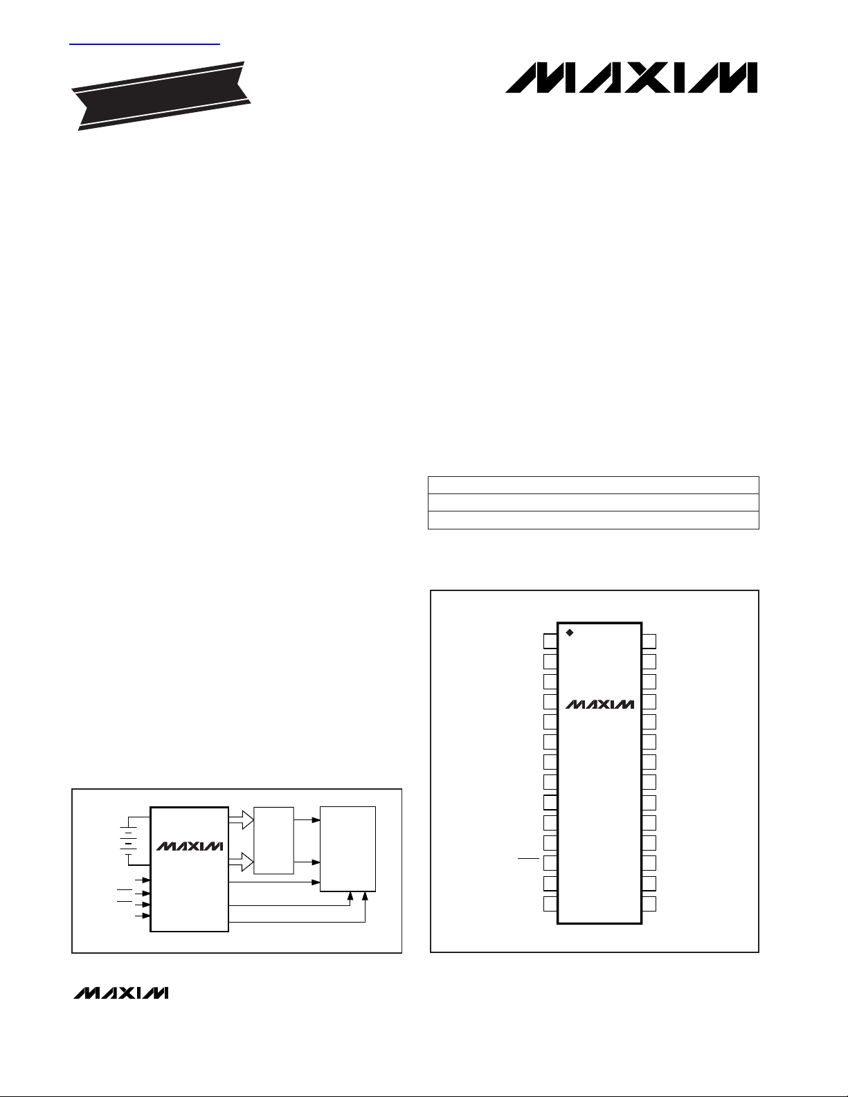
_____________________Pin Configuration
28
27
26
25
24
23
22
21
1
2
3
4
5
6
7
8
FB3
DH3
LX3
BST3
D1
ON3
SS3
CS3
TOP VIEW
DL3
V+
VL
FB5
Q1
Q2
VH
D2
20
19
18
17
9
10
11
12
PGND
DL5
BST5
LX5
SHDN
SYNC
REF
GND
SSOP
MAX786
16
15
13
14
DH5
CS5
SS5
ON5
Idle Mode is a trademark of Maxim Integrated Products. Pentium is a trademark of Intel Corp. PowerPC is a trademark of IBM Corp.
________Typical Application Diagram
MAX786
5.5V
TO
30V
SHUTDOWN
POWER
SECTION
POWER-GOOD
LOW-BATTERY WARNING
µP
MEMORY
PERIPHERALS
+3.3V
+5V
5V ON/OFF
3.3V ON/OFF
SYNC
SUSPEND POWER
28 SSOP0°C to +70°CMAX786RCAI
28 SSOP0°C to +70°CMAX786CAI
PIN-PACKAGETEMP. RANGEPART
3.45V
3.3V
V
OUT
Ordering Information continued at end of data sheet.
EVALUATION KIT
INFORMATION INCLUDED
For free samples & the latest literature: http://www.maxim-ic.com, or phone 1-800-998-8800.
For small orders, phone 1-800-835-8769.
查询MAX786S供应商
MAX786
Dual-Output Power-Supply
Controller for Notebook Computers
2 ________________________________________________________________________________________________
Stresses beyond those listed under “Absolute Maximum Ratings” may cause permanent damage to the device. These are stress ratings only, and functional
operation of the device at these or any other conditions beyond those indicated in the operational sections of the specifications is not implied. Exposure to
absolute maximum rating conditions for extended periods may affect device reliability.
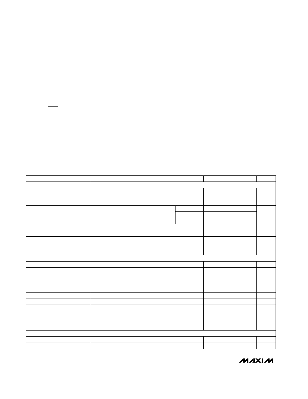
ELECTRICAL CHARACTERISTICS
(V+ = 15V, GND = PGND = 0V, IVL= I
REF
= 0mA,
SHDN
= ON3 = ON5 = 5V, other digital input levels are 0V or +5V,
T
A
= T
MIN
to T
MAX
, unless otherwise noted.)
ABSOLUTE MAXIMUM RATINGS
V+ to GND................................................................-0.3V to 36V
PGND to GND.......................................................................±2V
VL to GND..................................................................-0.3V to 7V
BST3, BST5 to GND.................................................-0.3V to 36V
LX3 to BST3 ...............................................................-7V to 0.3V
LX5 to BST5 ...............................................................-7V to 0.3V
Inputs/Outputs to GND
(D1, D2,
SHDN
, ON5, REF, SS5, CS5,
FB5, SYNC, CS3,FB3, SS3, ON3)............-0.3V to (VL + 0.3V)
VH to GND ...............................................................-0.3V to 20V
Q1, Q2 to GND............................................-0.3V to (VH + 0.3V)
DL3, DL5 to PGND.......................................-0.3V to (VL + 0.3V)
DH3 to LX3 ..............................................-0.3V to (BST3 + 0.3V)
DH5 to LX5 ..............................................-0.3V to (BST5 + 0.3V)
REF, VL Short to GND................................................Momentary
REF Current........................................................................20mA
VL Current ..........................................................................50mA
Continuous Power Dissipation (T
A
= +70°C)
SSOP (derate 9.52mW/°C above +70°C)....................762mW
Operating Temperature Ranges
MAX786CAI/MAX786_CAI .................................0°C to +70°C
MAX786EAI/MAX786_EAI...............................-40°C to +85°C
Lead Temperature (soldering, 10sec) ............................+300°C
MAX786S
MAX786R
MAX786
FB3 Output Voltage
3.46 3.65 3.75
V
0mV < (CS3-FB3) < 70mV, 6V < V + < 30V
(includes load and line regulation)
3.32 3.50 3.60
REF Load Regulation 30 75 mV0mA < IL< 5mA (Note 2)
PARAMETER
VL Output Voltage
MIN TYP MAX
4.5 5.5
UNITS
Current-Limit Voltage
V
80 100 120
VL Fault Lockout Voltage
mV
Line Regulation
3.6 4.2
0.03 %/V
Load Regulation 2.5
V
%
3.17 3.35 3.46
VL/FB5 Switchover Voltage
SS3/SS5 Source Current 2.5 4.0 6.5 µA
4.2 4.7 V
REF Output Voltage
SS3/SS5 Fault Sink Current 2
3.24 3.36
mA
V
REF Fault Lockout Voltage 2.4 3.2 V
Input Supply Range 5.5 30 V
FB5 Output Voltage 4.80 5.08 5.20 V
CONDITIONS
ON5 = ON3 = 0V, 5.5V < V+ < 30V, 0mA < IL< 25mA
CS3-FB3 or CS5-FB5
Falling edge, hysteresis = 1%
Either controller (V+ = 6V to 30V)
Either controller (CS_ -FB_ = 0mV to 70mV)
Rising edge of FB5, hysteresis = 1%
No external load (Note 1)
0mV < (CS5-FB5) < 70mV, 6V < V + < 30V
(includes load and line regulation)
Falling edge
V+ Shutdown Current 25 40 µA
–S—H—D—N–
= D1 = D2 = ON3 = ON5 = 0V, V+ = 30V
V+ Standby Current 70 120 µAD1 = D2 = ON3 = ON5 = 0V, V+ = 30V
Quiescent Power Consumption
(both PWM controllers on)
5.5 8.6 mW
D1 = D2 = 0V, FB5 = CS5 = 5.25V,
FB3 = CS3 = 3.5V
V+ Off Current 30 60 µAFB5 = CS5 = 5.25V, VL switched over to FB5
D1, D2 Trip Voltage 1.61 1.69 VFalling edge, hysteresis = 1%
D1, D2 Input Current ±100 nAD1 = D2 = 0V, 5V
3.3V AND 5V STEP-DOWN CONTROLLERS
INTERNAL REGULATOR AND REFERENCE
COMPARATORS
MAX786
Dual-Output Power-Supply
Controller for Notebook Computers
_________________________________________________________________________________________________
3
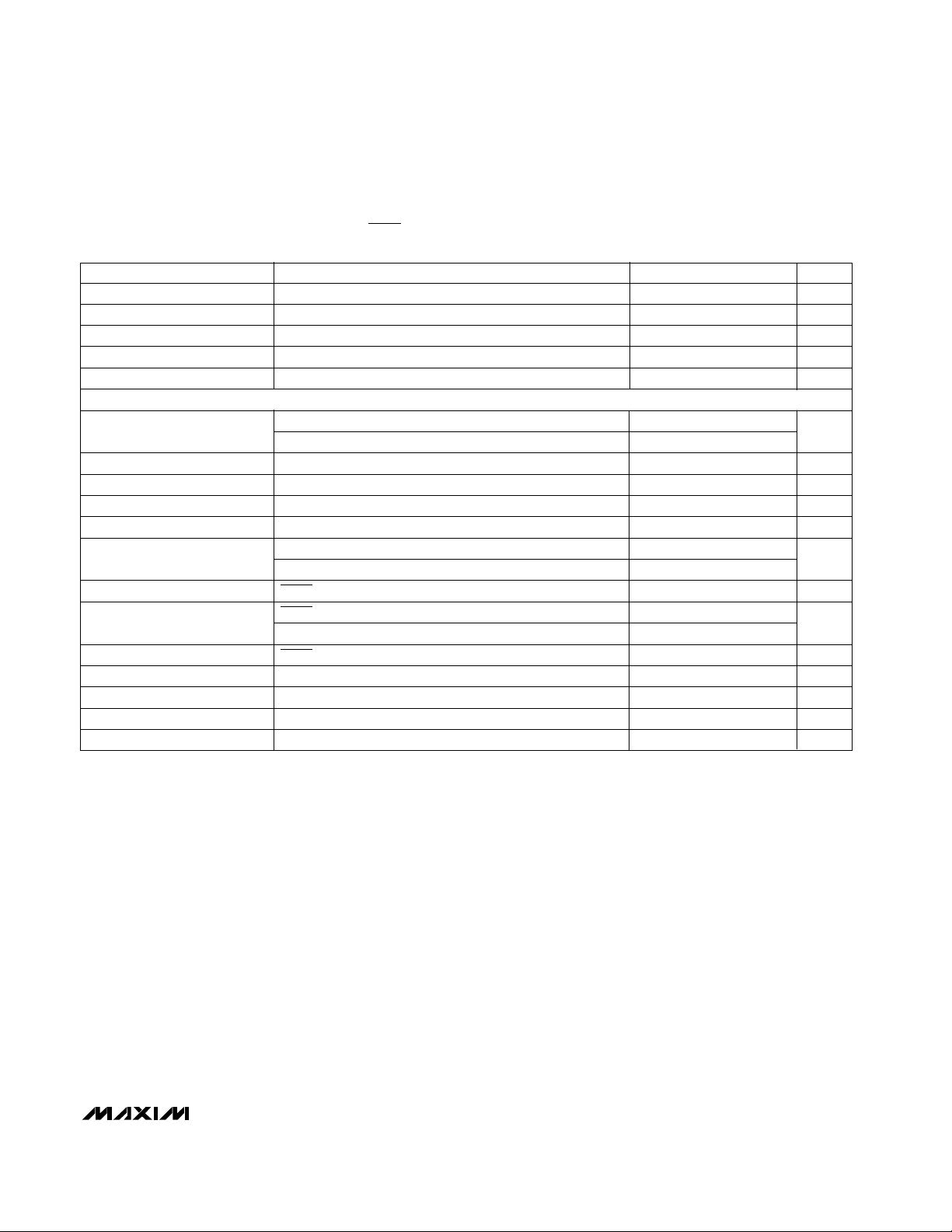
Note 1: Since the reference uses VL as its supply, its V+ line regulation error is insignificant.
Note 2: The main switching outputs track the reference voltage. Loading the reference reduces the main outputs slightly according
to the closed-loop gain (AV
CL
) and the reference voltage load-regulation error. AVCLfor the +3.3V supply is unity gain.
AVCLfor the +5V supply is 1.54.
PARAMETER CONDITIONS MIN TYP MAX UNITS
Q1, Q2 Source Current VH = 15V, V
OUT
= 2.5V 12 20 30 µA
Q1, Q2 Sink Current VH = 15V, V
OUT
= 2.5V 200 500 1000 µA
Q1, Q2 Output High Voltage I
SOURCE
= 5µA, VH = 3V VH -0.5 V
Q1, Q2 Output Low Voltage I
SINK
= 20µA, VH = 3V 0.4 V
Quiescent VH Current VH = 18V, D1 = D2 = 5V, no external load 4 10 µA
OSCILLATOR AND INPUTS/OUTPUTS
Oscillator Frequency
SYNC = 3.3V 270 300 330
kHz
SYNC = 0V, 5V 170 200 230
SYNC High Pulse Width 200 ns
SYNC Low Pulse Width 200 ns
SYNC Rise/Fall Time Not tested 200 ns
Oscillator SYNC Range 240 350 kHz
Maximum Duty Cycle
SYNC = 3.3V 89 92
%
SYNC = 0V or 5V 92 95
Input Low Voltage
SHDN
, ON3, ON5, SYNC 0.8 V
Input High Voltage
SHDN
, ON3, ON5 2.4
V
SYNC VL -0.5
Input Current
SHDN
, ON3, ON5 VIN= 0V, 5V ±1 µA
DL3/DL5 Sink/Source Current V
OUT
= 2V 1 A
DH3/DH5 Sink/Source Current BST3-LX3 = BST5-LX5 = 4.5V, V
OUT
= 2V 1 A
DL3/DL5 On-Resistance High or low 7 Ω
DH3/DH5 On-Resistance High or low, BST3-LX3 = BST5-LX5 = 4.5V 7 Ω
ELECTRICAL CHARACTERISTICS (continued)
(V+ = 15V, GND = PGND = 0V, IVL= I
REF
= 0mA,
SHDN
= ON3 = ON5 = 5V, other digital input levels are 0V or +5V,
T
A
= T
MIN
to T
MAX
, unless otherwise noted.)
MAX786
Dual-Output Power-Supply
Controller for Notebook Computers
4 _______________________________________________________________________________________
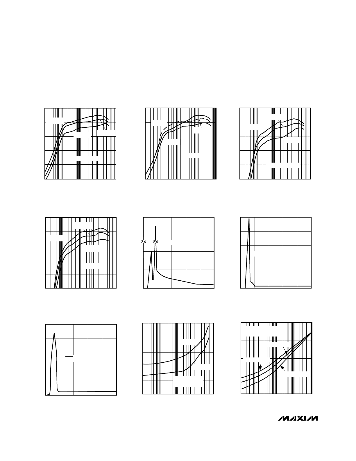
________________________________________________Typical Operating Characteristics
(Circuit of Figure 1, TA = +25°C, unless otherwise noted.)
EFFICIENCY vs. +5V OUTPUT
CURRENT, 300kHz
EFFICIENCY (%)
50
60
70
80
90
100
1m 10m 100m 1 10
+5V OUTPUT CURRENT (A)
VIN = 6V
VIN = 15V
VIN = 30V
+3.3V OFF
EFFICIENCY vs. +3.3V OUTPUT
CURRENT, 200kHz
EFFICIENCY (%)
50
60
70
80
90
100
1m
10m 100m 1 10
+3.3V OUTPUT CURRENT (A)
VIN = 6V
VIN = 15V
VIN = 30V
SYNC = 0V, +5V ON
EFFICIENCY vs. +3.3V OUTPUT
CURRENT, 300kHz
EFFICIENCY (%)
50
60
70
80
90
100
1m 10m 100m 1 10
+3.3V OUTPUT CURRENT (A)
VIN = 6V
VIN = 15V
VIN = 30V
+5V ON
SHUTDOWN SUPPLY CURRENT vs.
SUPPLY VOLTAGE
SHUTDOWN SUPPLY CURRENT (µA)
0
100
200
300
400
500
0
6 12 18 24 30
SUPPLY VOLTAGE (V)
SHDN = 0V
QUIESCENT SUPPLY CURRENT vs.
SUPPLY VOLTAGE
QUIESCENT SUPPLY CURRENT (mA)
0
1
2
18
19
0 6 12 18 24 30
SUPPLY VOLTAGE (V)
ON3 = ON5 = HIGH
STANDBY SUPPLY CURRENT vs.
SUPPLY VOLTAGE
STANDBY SUPPLY CURRENT (mA)
0
0.5
1.0
1.5
2.0
2.5
0 6 12 18 24 30
ON3 = ON5 = 0V
SUPPLY VOLTAGE (V)
MINIMUM VIN TO V
OUT
DIFFERENTIAL
vs. +5V OUTPUT CURRENT
MINIMUM V
IN
TO V
OUT
DIFFERENTIAL (V)
+5V OUTPUT CURRENT (A)
0
0.2
0.4
0.6
0.8
1.0
1m 10m 100m 1 10
300kHz
200kHz
+5V OUTPUT
STILL REGULATING
EFFICIENCY vs. +5V OUTPUT
CURRENT, 200kHz
EFFICIENCY (%)
50
60
70
80
90
100
1m 10m 100m 1 10
+5V OUTPUT CURRENT (A)
VIN = 6V
VIN = 30V
VIN = 15V
SYNC = 0V, +3.3V OFF
1000
0.1
100µ 10m 1
SWITCHING FREQUENCY vs.
LOAD CURRENT
10
LOAD CURRENT (A)
SWITCHING FREQUENCY (kHz)
100
1m 100m
SYNC = REF (300kHz)
ON3 = ON5 = 5V
+5V, VIN = 7.5V
1
+5V, VIN = 30V
+3.3V, VIN = 7.5V
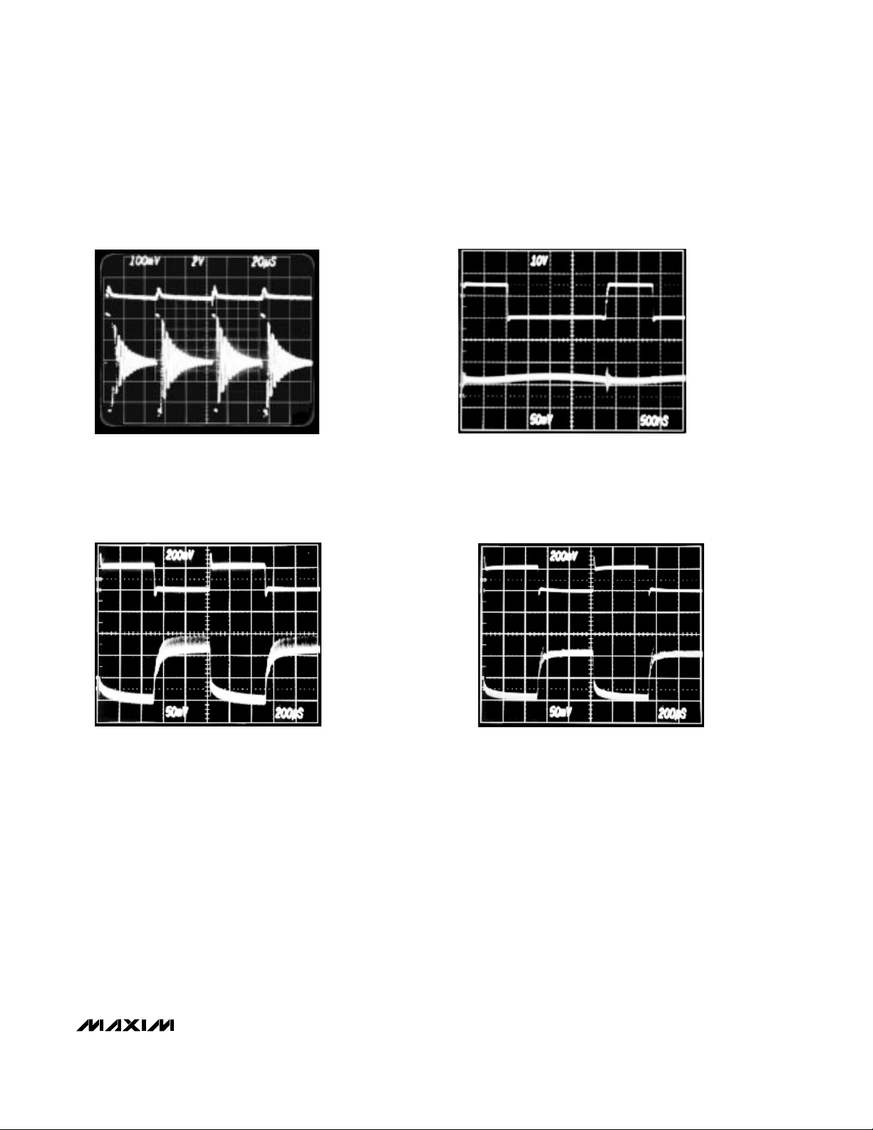
200µs/div
I
LOAD
= 100mA
V
IN
= 10V
IDLE MODE WAVEFORMS
+5V OUTPUT
50mV/div
2V/div
MAX786
Dual-Output Power-Supply
Controller for Notebook Computers
_______________________________________________________________________________________ 5
500ns/div
+5V OUTPUT CURRENT = 1A
V
IN
= 16V
PULSE-WIDTH MODULATION MODE WAVEFORMS
LX 10V/div
+5V OUTPUT
50mV/div
200µs/div
V
IN
= 15V
+3.3V LOAD-TRANSIENT RESPONSE
+3.3V OUTPUT
50mV/div
3A
0A
LOAD CURRENT
200µs/div
V
IN
= 15V
+5V LOAD-TRANSIENT RESPONSE
+5V OUTPUT
50mV/div
3A
0A
LOAD CURRENT
_________________________________Typical Operating Characteristics (continued)
(Circuit of Figure 1, TA = +25°C, unless otherwise noted.)
MAX786
Dual-Output Power-Supply
Controller for Notebook Computers
6 _______________________________________________________________________________________
_________________________________Typical Operating Characteristics (continued)
(Circuit of Figure 1, TA = +25°C, unless otherwise noted.)
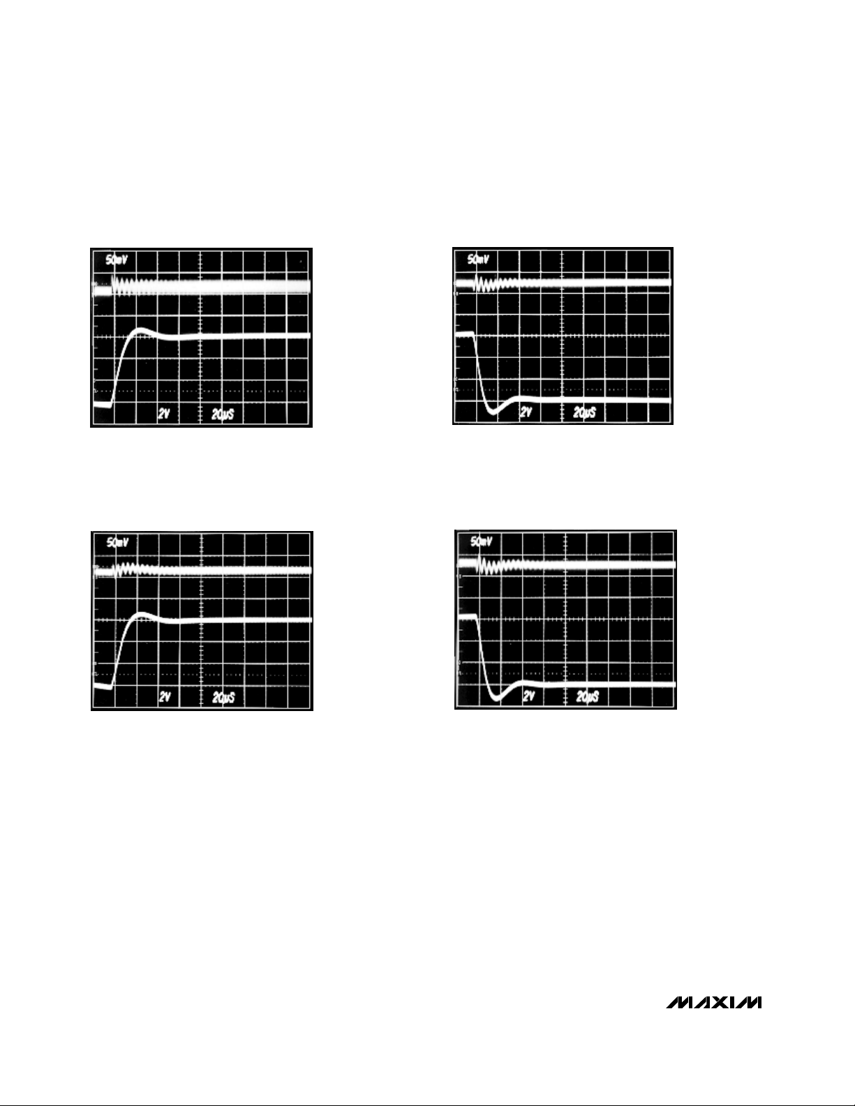
20µs/div
I
LOAD
= 2A
+5V LINE-TRANSIENT RESPONSE, RISING
VIN, 10V TO 16V
2V/div
+5V OUTPUT
50mV/div
20µs/div
I
LOAD
= 2A
+5V LINE-TRANSIENT RESPONSE, FALLING
VIN, 16V TO 10V
2V/div
+5V OUTPUT
50mV/div
20µs/div
I
LOAD
= 2A
+3.3V LINE-TRANSIENT RESPONSE, RISING
+3.3V OUTPUT
50mV/div
V
IN
, 10V TO 16V
2V/div
20µs/div
I
LOAD
= 2A
+3.3V LINE-TRANSIENT RESPONSE, FALLING
+3.3V OUTPUT
50mV/div
V
IN
, 16V TO 10V
2V/div
 Loading...