

19-0176; Rev 0; 6/94
Evaluation Kit
Available
High-Efficiency, Low IQDC-DC Inverters
-5V/-12V/-15V or Adjustable,
_______________General Description
The MAX764/MAX765/MAX766 inverting switching regulators are highly efficient over a wide range of load currents, delivering up to 1.5W. A unique, current-limited,
pulse-frequency-modulated (PFM) control scheme combines the benefits of traditional PFM converters with the
benefits of pulse-width-modulated (PWM) converters.
Like PWM converters, the MAX764/MAX765/MAX766 are
highly efficient at heavy loads. Yet because they are PFM
devices, they use less than 120µA of supply current (vs.
2mA to 10mA for a PWM device).
The input voltage range is 3V to 16V. The output voltage is preset at -5V (MAX764), -12V (MAX765), or -15V
(MAX766); it can also be adjusted from -1V to -16V
using two external resistors (Dual ModeTM). The maximum operating VIN- V
differential is 20V.
OUT
These devices use miniature external components; their
high switching frequencies (up to 300kHz) allow for less
than 5mm diameter surface-mount magnetics. A standard 47µH inductor is ideal for most applications, so no
magnetics design is necessary.
An internal power MOSFET makes the MAX764/MAX765/
MAX766 ideal for minimum component count, low- and
medium-power applications. For increased output drive
capability or higher output voltages, use the
MAX774/MAX775/MAX776 or MAX1774, which drive an
external power P-channel MOSFET for loads up to 5W.
________________________Applications
LCD-Bias Generators
Portable Instruments
LAN Adapters
Remote Data-Acquisition Systems
Battery-Powered Applications
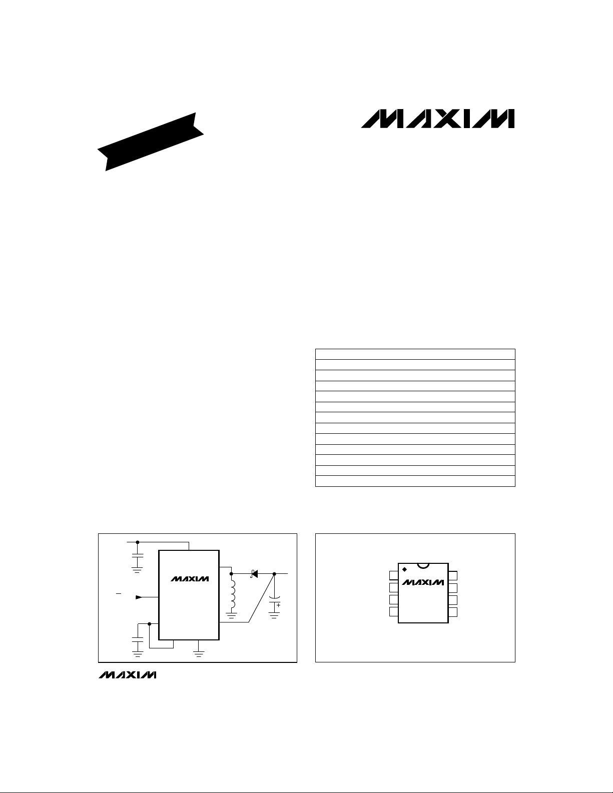
__________Typical Operating Circuit
____________________________Features
♦ High Efficiency for a Wide Range of Load Currents
♦ 250mA Output Current
♦ 120µA Max Supply Current
♦ 5µA Max Shutdown Current
♦ 3V to 16V Input Voltage Range
♦ -5V (MAX764), -12V (MAX765), -15V (MAX766),
or Adjustable Output from -1V to -16V
♦ Current-Limited PFM Control Scheme
♦ 300kHz Switching Frequency
♦ Internal, P-Channel Power MOSFET
______________Ordering Information
PART
MAX764CPA
MAX764CSA
MAX764C/D 0°C to +70°C
MAX764EPA
MAX764ESA -40°C to +85°C
MAX764MJA -55°C to +125°C 8 CERDIP**
MAX765CPA
MAX765CSA
MAX765C/D 0°C to +70°C
MAX765EPA
MAX765ESA -40°C to +85°C
MAX765MJA -55°C to +125°C 8 CERDIP**
Ordering Information continued on last page.
* Dice are tested at T
**Contact factory for availability and processing to MIL-STD-883.
TEMP. RANGE PIN-PACKAGE
0°C to +70°C
0°C to +70°C
-40°C to +85°C 8 Plastic DIP
0°C to +70°C 8 Plastic DIP
0°C to +70°C
-40°C to +85°C 8 Plastic DIP
= +25°C, DC parameters only.
A
8 Plastic DIP
8 SO
Dice*
8 SO
8 SO
Dice*
8 SO
__________________Pin Configuration
MAX764/MAX765/MAX766
INPUT
3V TO 15V
ON/OFF
V+
LX
MAX764
SHDN
REF
FB
________________________________________________________________
OUT
GND
47µH
OUTPUT
-5V
TOP VIEW
OUT
SHDN
REF
1
FB
2
MAX764
MAX765
3
MAX766
4
DIP/SO
Maxim Integrated Products
Call toll free 1-800-998-8800 for free samples or literature.
LX
8
V+
7
V+
6
GND
5
1
-5V/-12V/-15V or Adjustable,
High-Efficiency, Low IQDC-DC Inverters
ABSOLUTE MAXIMUM RATINGS
V+ to GND..............................................................-0.3V to +17V
OUT to GND...........................................................+0.5V to -17V
Maximum Differential (V+ to OUT) ......................................+21V
REF, SHDN, FB to GND ...............................-0.3V to (V+ + 0.3V)
LX to V+..................................................................+0.3V to -21V
LX Peak Current ...................................................................1.5A
Continuous Power Dissipation (T
Plastic DIP (derate 9.09mW/°C above +70°C) ............727mW
SO (derate 5.88mW/°C above +70°C) .........................471mW
CERDIP (derate 8.00mW/°C above +70°C) .................640mW
Stresses beyond those listed under “Absolute Maximum Ratings” may cause permanent damage to the device. These are stress ratings only, and functional
operation of the device at these or any other conditions beyond those indicated in the operational sections of the specifications is not implied. Exposure to
absolute maximum rating conditions for extended periods may affect device reliability.
= +70°C)
A
ELECTRICAL CHARACTERISTICS
(V+ = 5V, I
V+ Input Voltage Range
Supply Current
Shutdown Current
MAX764/MAX765/MAX766
FB Input Current
Output Current and Voltage
(Note 1)
Reference Voltage
REF Load Regulation
Efficiency (Note 2)
SHDN Input Voltage High
SHDN Input Voltage Low
LOAD
= 0mA, C
= 0.1µF, TA= T
REF
to T
MIN
MAX76_C/E
V+ V
MAX76_M
V+ = 16V, SHDN < 0.4V
S
I
SHDN
I
V
V+ = 16V, SHDN > 1.6V
V+ = 10V, SHDN > 1.6V
3V ≤ V+ ≤ 16V
MAX76_C
MAX76_E
I
FB
MAX76_M
MAX764, -4.8V ≤ V
MAX765C/E, -11.52V ≤ V
OUT
MAX765M, -11.52V ≤ V
MAX766, -14.40V ≤ V
MAX76_C
MAX76_E
REF
MAX76_M
0µA ≤ I
3V ≤ V+ ≤ 16V
0mA ≤ I
4V ≤ V+ ≤ 6V
10mA ≤ I
VIN= 5V
V+ = 16V, SHDN = 0V or V+
3V ≤ V+ ≤ 16V
IH
3V ≤ V+ ≤ 16V V0.4V
IL
, unless otherwise noted. Typical values are at TA= +25°C.)
MAX
≤ 100µA
REF
LOAD
LOAD
Operating Temperature Ranges
MAX76_C_A ........................................................0°C to +70°C
MAX76_E_A .....................................................-40°C to +85°C
MAX76_MJA ..................................................-55°C to +125°C
Maximum Junction Temperatures
MAX76_C_A/E_A ..........................................................+150°C
MAX76_MJA .................................................................+175°C
Storage Temperature Range ............................-65°C to +160°C
Lead Temperature (soldering, 10sec) ............................+300°C
CONDITIONS
3.0 16.0
3.5
90 120I
2
15
OUT
≤ 100mA
≤ 100mA,
≤ 5.2V
OUT
OUT
≤ -15.60V
OUT
MAX76_C/E
MAX76_M
V
≤ 12.48V
≤ 12.48V
= -5V
OUT
= -15V
OUT
150 260
68 120
50 120
35 105
1.4700 1.5 1.5300
1.4625 1.5 1.5375 V
1.4550 1.5 1.5450
410
415
80
82V
±50
±70
±90
UNITSMIN TYP MAXSYMBOLPARAMETER
µA
mV-10 10FB Trip Point
nA
mA
mV
µV/V40 100REF Line Regulation
%/mA0.008Load Regulation (Note 2)
%/V0.12Line Regulation (Note 2)
%
µA±1SHDN Leakage Current
V1.6V
2 _______________________________________________________________________________________
-5V/-12V/-15V or Adjustable,
High-Efficiency, Low IQDC-DC Inverters
ELECTRICAL CHARACTERISTICS (continued)
(V+ = 5V, I
LX Leakage Current
Peak Current at LX
Maximum Switch On-Time
Minimum Switch Off-Time
Note 1: See Maximum Output Current vs. Supply Voltage graph in the
Note 2: Circuit of Figure 2.
LOAD
= 0mA, C
= 0.1µF, TA= T
REF
MIN
to T
, unless otherwise noted. Typical values are at TA= +25°C.)
MAX
CONDITIONS
MAX76_C
+ (V+) ≤ 20V
ILXI
MAX76_E
MAX76_M
V
+ (V+) ≥ 10V
OUT
I
I
V
PEAK
ON
OFF
OUT
I
+ (V+) ≥ 10V
I
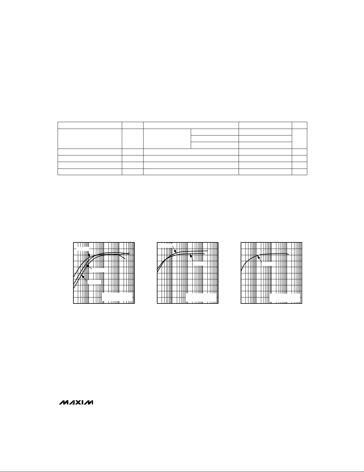
Typical Operating Characteristics
correlation to switch on-time, switch off-time, on-resistance, and peak current rating.
UNITSMIN TYP MAXSYMBOLPARAMETER
±5
±10 µA
±30
Ω1.4 2.5LX On-Resistance
A0.5 0.75I
µs12 16 20t
µs1.8 2.3 2.8t
. Guarantees are based on
__________________________________________Typical Operating Characteristics
(V+ = 5V, V
100
90
80
70
60
50
40
EFFICIENCY (%)
30
20
10
0
= -5V, TA= +25°C, unless otherwise noted.)
OUT
EFFICIENCY vs. LOAD CURRENT
V+ = 5V
0.1 10 1000
MAX764
V+ = 10V
V+ = 15V
CIRCUIT OF FIGURE 2
= -5V ±4%
V
OUT
1 100
LOAD CURRENT (mA)
MAX764-01
EFFICIENCY vs. LOAD CURRENT
100
V+ = 8V
90
80
70
60
50
40
EFFICIENCY (%)
30
20
10
0
0.1 10 1000
MAX765
V+ = 5V
CIRCUIT OF FIGURE 2
= -12V ±4%
V
OUT
1 100
LOAD CURRENT (mA)
MAX764-02
EFFICIENCY vs. LOAD CURRENT
100
90
80
70
60
50
40
EFFICIENCY (%)
30
20
10
0
0.1 10 1000
MAX766
V+ = 5V
CIRCUIT OF FIGURE 2
= -15V ±4%
V
OUT
1 100
LOAD CURRENT (mA)
MAX764/MAX765/MAX766
MAX764-03
_______________________________________________________________________________________ 3
-5V/-12V/-15V or Adjustable,
High-Efficiency, Low IQDC-DC Inverters
____________________________Typical Operating Characteristics (continued)
(V+ = 5V, V
= -5V, TA= +25°C, unless otherwise noted.)
OUT
MAXIMUM OUTPUT CURRENT
600
500
400
300
200
100
MAXIMUM OUTPUT CURRENT (mA)
0
4.0
3.5
MAX764/MAX765/MAX766
3.0
2.5
2.0
1.5
1.0
SHUTDOWN CURRENT (µA)
0.5
0
7.2
7.1
7.0
6.9
6.8
6.7
6.6
6.5
6.4
SWITCH ON/OFF-TIME RATIO (µs/µs)
6.3
6.2
vs. SUPPLY VOLTAGE
CIRCUIT OF FIGURE 2
V
= -5V
OUT
V
= -12V
OUT
V
= -15V
OUT
3
4 5 6 7 8 9 10 11 12 13 14 15 16
SUPPLY VOLTAGE (V)
SHUTDOWN CURRENT
vs. TEMPERATURE
V+ = 15V
V+ = 8V
V+ = 4V
-60
-40 -20 0 20 40 60 80 100 120 140
TEMPERATURE (°C)
SWITCH ON/OFF-TIME RATIO
vs. TEMPERATURE
V+ = 5V
-60
-40 -20 0 20 40 60 80 100 120 140
TEMPERATURE (°C)
MAX764 -04
NO-LOAD SUPPLY CURRENT (µA)
MAX764 -07
MAXIMUM SWITCH ON-TIME (µs)
MAX764 -10
START-UP SUPPLY VOLTAGE (V)
NO-LOAD SUPPLY CURRENT
100
95
90
85
80
75
70
65
60
17.0
16.8
16.6
16.4
16.2
16.0
15.8
15.6
15.4
15.2
15.0
vs. SUPPLY VOLTAGE
3
4 5 6 7 8 9 10 11 12 13 14 15 16
SUPPLY VOLTAGE (V)
MAXIMUM SWITCH ON-TIME
vs. TEMPERATURE
V+ = 5V
-60
-40 -20 0 20 40 60 80 100 120 140
TEMPERATURE (°C)
START-UP SUPPLY VOLTAGE
8
7
6
5
4
3
2
1
0
vs. OUTPUT CURRENT
CIRCUIT OF FIGURE 2
0
50 100 150 200 250 300
OUTPUT CURRENT (mA)
V+ = 15V
110
105
MAX764 -05
100
95
90
85
80
75
70
65
60
NO-LOAD SUPPLY CURRENT (µA)
55
50
-60
-40 -20 0 20 40 60 80 100 120 140
2.60
2.55
MAX764 -08
2.50
2.45
2.40
2.35
2.30
MINIMUM SWITCH OFF-TIME (µs)
2.25
2.20
-60
10,000
MAX764 -11
1000
100
10
LX LEAKAGE CURRENT (nA)
1
20
NO-LOAD SUPPLY CURRENT
vs. TEMPERATURE
V+ = 15V
V+ = 5V
TEMPERATURE (°C)
MINIMUM SWITCH OFF-TIME
vs. TEMPERATURE
V+ = 15V
V+ = 5V
-40 -20 0 20 40 60 80 100 120 140
TEMPERATURE (°C)
LX LEAKAGE CURRENT
vs. TEMPERATURE
IV
I + (V+) = 20V
OUT
30 40 50 60 70 80 90 100 110 120 130
TEMPERATURE (°C)
MAX764 -06
MAX764 -09
MAX764-12
4 _______________________________________________________________________________________

-5V/-12V/-15V or Adjustable,
MAX764
14
0
High-Efficiency, Low IQDC-DC Inverters
____________________________Typical Operating Characteristics (continued)
(V+ = 5V, V
2.2
2.0
1.8
1.6
1.4
1.2
LX ON-RESISTANCE (Ω)
1.0
0.8
= -5V, TA= +25°C, unless otherwise noted.)
OUT
LX ON-RESISTANCE
vs. TEMPERATURE
IV
I + (V+) = 10V
OUT
IV
I + (V+) = 15V
OUT
IV
I + (V+) = 20V
OUT
-60
-40 -20 0 20 40 60 80 100 120 140
TEMPERATURE (°C)
REFERENCE OUTPUT
1.506
1.504
1.502
1.500
1.498
1.496
REFERENCE OUTPUT (V)
1.494
1.492
-60
vs. TEMPERATURE
-40 -20 0 20 40 60 80 100 120 140
TEMPERATURE (°C)
0.95
MAX764 -13
0.90
0.85
0.80
0.75
CURRENT AT LX (A)
0.70
0.65
PEAK CURRENT AT LX
vs. TEMPERATURE
IV
I + (V+) = 20V
OUT
IV
I + (V+) = 15V
OUT
IV
I + (V+) = 10V
OUT
-40 -20 0 20 40 60 80 100 120 14
-60
TEMPERATURE (°C)
MAX764 -16
1000
100
10
1
SUPPLY CURRENT (mA)
0.1
0.01
REFERENCE OUTPUT RESISTANCE
250
-
200
150
100
50
REFERENCE OUTPUT RESISTANCE (Ω)
0
-60
SUPPLY CURRENT
vs. SUPPLY VOLTAGE
0 2 4 6 10 12 14816
SUPPLY VOLTAGE (V)
vs. TEMPERATURE
I
= 10µA
REF
I
= 50µA
REF
I
= 100µA
REF
-40 -20 0 20 40 60 80 100 120 140
TEMPERATURE (°C)
I
= 100mA
LOAD
I
= 0mA
LOAD
CIRCUIT OF FIGURE 2
MAX764-17
MAX764/MAX765/MAX766
MAX764 -15
_______________________________________________________________________________________
5

-5V/-12V/-15V or Adjustable,
High-Efficiency, Low IQDC-DC Inverters
____________________________Typical Operating Characteristics (continued)
(V+ = 5V, V
= -5V, TA= +25°C, unless otherwise noted.)
OUT
TIME TO ENTER/EXIT SHUTDOWN
0V
A
0V
CIRCUIT OF FIGURE 2, V+ = 5V, I
A: V
, 2V/div
OUT
B: SHUTDOWN PULSE, 0V TO 5V, 5V/div
2ms/div
LOAD
= 100mA, V
OUT
B
= -5V
MAX764/MAX765/MAX766
LINE-TRANSIENT RESPONSE
A
B
0V
LOAD-TRANSIENT RESPONSE
0mA
CIRCUIT OF FIGURE 2, V+ = 5V, V
A: V
, 50mV/div, AC-COUPLED
OUT
B: I
, 0mA TO 100mA, 100mA/div
LOAD
DISCONTINUOUS CONDUCTION AT
HALF AND FULL CURRENT LIMIT
0A
0V
5ms/div
A
B
= -5V
OUT
A
B
C
CIRCUIT OF FIGURE 2, V
A: V
, 50mV/div, AC-COUPLED
OUT
B: V+, 5V TO 10V, 5V/div
OUT
5ms/div
= -5V, I
LOAD
= 100mA
CIRCUIT OF FIGURE 2, V+ = 5V, V
A: OUTPUT RIPPLE, 100mV/div
B: INDUCTOR CURRENT, 500mA/div
C: LX WAVEFORM, 10V/div
5µs/div
OUT
= -5V, I
6 _______________________________________________________________________________________
LOAD
= 140mA

-5V/-12V/-15V or Adjustable,
High-Efficiency, Low IQDC-DC Inverters
____________________________Typical Operating Characteristics (continued)
(V+ = 5V, V
0A
0V
= -5V, TA= +25°C, unless otherwise noted.)
OUT
DISCONTINUOUS CONDUCTION AT
HALF CURRENT LIMIT
CIRCUIT OF FIGURE 2, V+ = 5V, V
A: OUTPUT RIPPLE, 100mV/div
B: INDUCTOR CURRENT, 500mA/div
C: LX WAVEFORM, 10V/div
5µs/div
OUT
= -5V, I
LOAD
= 80mA
CONTINUOUS CONDUCTION AT
FULL CURRENT LIMIT
A
B
C
0A
0V
CIRCUIT OF FIGURE 2, V+ = 5V, V
A: OUTPUT RIPPLE, 100mV/div
B: INDUCTOR CURRENT, 500mA/div
C: LX WAVEFORM, 10V/div
5µs/div
= -5V, I
LOAD
= 240mA
OUT
A
B
C
______________________________________________________________Pin Description
PIN
Sense Input for Fixed-Output Operation (VFB= V
FB2
SHDN3
Feedback Input. Connect FB to REF to use the internal voltage divider for a preset output. For adjustableoutput operation, use an external voltage divider, as described in the section
Active-High Shutdown Input. With SHDN high, the part is in shutdown mode and the supply current is less
than 5µA. Connect to ground for normal operation.
1.5V Reference Output that can source 100µA for external loads. Bypass to ground with a 0.1µF capacitor.REF4
GroundGND5
V+6, 7
Positive Power-Supply Input. Must be tied together. Place a 0.1µF input bypass capacitor as close to
the V+ and GND pins as possible.
Drain of the Internal P-Channel Power MOSFET. LX has a peak current limit of 0.75A.LX8
FUNCTIONNAME
). OUT must be connected to V
REF
.OUT1
OUT
Setting the Output Voltage.
MAX764/MAX765/MAX766
_______________________________________________________________________________________ 7

-5V/-12V/-15V or Adjustable,
High-Efficiency, Low IQDC-DC Inverters
FB
COMPARATOR
REF
SHDN
MAX764/MAX765/MAX766
Figure 1. Block Diagram
ERROR
COMPARATOR
TRIG Q
ONE-SHOT
ONE-SHOT
TRIGQ
SRQ
CURRENT
CONTROL CIRCUITS
_______________Detailed Description
The MAX764/MAX765/MAX766 are BiCMOS, inverting,
switch-mode power supplies that provide fixed outputs
of -5V, -12V, and -15V, respectively; they can also be
set to any desired output voltage using an external
resistor divider. Their unique control scheme combines
the advantages of pulse-frequency modulation (pulse
skipping) and pulse-width modulation (continuous pulsing). The internal P-channel power MOSFET allows
peak currents of 0.75A, increasing the output current
capability over previous pulse-frequency-modulation
(PFM) devices. Figure 1 shows the MAX764/MAX765/
MAX766 block diagram.
The MAX764/MAX765/MAX766 offer three main
improvements over prior solutions:
Operating Principle
MAX764
MAX765
MAX766
N
1.5V
REFERENCE
FROM V+
P
COMPARATOR
GND
CURRENT
FROM OUT
(FULL
CURRENT)
0.2V
0.1V
(HALF
CURRENT)
FROM V+
1) They can operate with miniature (less than 5mm
diameter) surface-mount inductors, because of their
300kHz switching frequency.
2) The current-limited PFM control scheme allows efficiencies exceeding 80% over a wide range of load currents.
3) Maximum quiescent supply current is only 120µA.
Figures 2 and 3 show the standard application circuits
for these devices. In these configurations, the IC is
powered from the total differential voltage between the
input (V+) and output (V
). The principal benefit of
OUT
this arrangement is that it applies the largest available
signal to the gate of the internal P-channel power MOSFET. This increased gate drive lowers switch on-resistance and increases DC-DC converter efficiency.
Since the voltage on the LX pin swings from V+ (when the
switch is ON) to IV
plus a diode drop (when the
OUT
I
OUT
V+
V+
LX
8 _______________________________________________________________________________________

-5V/-12V/-15V or Adjustable,
High-Efficiency, Low IQDC-DC Inverters
switch is OFF), the range of input and output voltages is
limited to a 21V absolute maximum differential voltage.
When output voltages more negative than -16V are
required, substitute the MAX764/MAX765/MAX766 with
Maxim’s MAX774/MAX775/MAX776 or MAX1774, which
use an external switch.
V
IN
-12
-15
5
-5
GND
V+
V+
LX
47µH
7
6
8
L1
INPUT
VOLTAGE (V)
3 to 15
3 to 8
3 to 5
7
V+
6
V+
8
LX
L1
47µH
D1
1N5817
1N5817
V
OUT
C4
68µF
20V
V
OUT
D1
-1V to
-16V
C4
68µF
20V
1
OUT
C2
C1
120µF
20V
0.1µF
3
MAX764
SHDN
MAX765
MAX766
2
FB
4
REF
GND
5
OUTPUT
VOLTAGE (V)
0.1µF
C3
PRODUCT
MAX764
MAX765
MAX766
Figure 2. Fixed Output Voltage Operation
V
IN
C1
120µF
20V
C2
0.1µF
R2
1
OUT
3
MAX764
SHDN
MAX765
MAX766
2
FB
R1
4
REF
C3
0.1µF
Figure 3. Adjustable Output Voltage Operation
_______________________________________________________________________________________ 9
The MAX764/MAX765/MAX766 use a proprietary, cur-
PFM Control Scheme
rent-limited PFM control scheme that blends the best
features of PFM and PWM devices. It combines the
ultra-low supply currents of traditional pulse-skipping
PFM converters with the high full-load efficiencies of
current-mode pulse-width modulation (PWM) converters. This control scheme allows the devices to achieve
high efficiencies over a wide range of loads, while the
current-sense function and high operating frequency
allow the use of miniature external components.
As with traditional PFM converters, the internal power
MOSFET is turned on when the voltage comparator
senses that the output is out of regulation (Figure 1).
However, unlike traditional PFM converters, switching is
accomplished through the combination of a peak current limit and a pair of one-shots that set the maximum
on-time (16µs) and minimum off-time (2.3µs) for the
switch. Once off, the minimum off-time one-shot holds
the switch off for 2.3µs. After this minimum time, the
switch either 1) stays off if the output is in regulation, or
2) turns on again if the output is out of regulation.
The MAX764/MAX765/MAX766 limit the peak inductor
current, which allows them to run in continuous-conduction mode and maintain high efficiency with heavy
loads. (See the photo Continuous Conduction at Full
Current Limit in the
Typical Operating Characteristics
This current-limiting feature is a key component of the
control circuitry. Once turned on, the switch stays on
until either 1) the maximum on-time one shot turns it off
(16µs later), or 2) the current limit is reached.
To increase light-load efficiency, the current limit is set to
half the peak current limit for the first two pulses. If those
pulses bring the output voltage into regulation, the voltage comparator holds the MOSFET off and the current
limit remains at half the peak current limit. If the output
voltage is still out of regulation after two pulses, the current limit is raised to its 0.75A peak for the next pulse.
(See the photo Discontinuous Conduction at Half and Full
Current Limit in the
Typical Operating Characteristics
.)
Shutdown Mode
When SHDN is high, the MAX764/MAX765/MAX766
enter a shutdown mode in which the supply current
drops to less than 5µA. In this mode, the internal biasing
circuitry (including the reference) is turned off and OUT
discharges to ground. SHDN is a TTL/CMOS-logic level
input. Connect SHDN to GND for normal operation.
With a current-limited supply, power-up the device while
unloaded or in shutdown mode (hold SHDN high until V+
exceeds 3.0V) to save power and reduce power-up current surges. (See the Supply Current vs. Supply Voltage
graph in the
Typical Operating Characteristics
.)
MAX764/MAX765/MAX766
.)

-5V/-12V/-15V or Adjustable,
High-Efficiency, Low IQDC-DC Inverters
When delivering high output currents, the MAX764/
MAX765/MAX766 operate in continuous-conduction
mode. In this mode, current always flows in the inductor, and the control circuit adjusts the duty-cycle of the
switch on a cycle-by-cycle basis to maintain regulation
without exceeding the switch-current capability. This
provides excellent load-transient response and high
efficiency.
In discontinuous-conduction mode, current through the
inductor starts at zero, rises to a peak value, then
ramps down to zero on each cycle. Although efficiency
is still excellent, the output ripple may increase slightly.
__________________Design Procedure
Modes of Operation
The MAX764/MAX765/MAX766’s output voltage can be
adjusted from -1.0V to -16V using external resistors R1
and R2, configured as shown in Figure 3. For
adjustable-output operation, select feedback resistor
R1 = 150kΩ. R2 is given by:
MAX764/MAX765/MAX766
where V
For fixed-output operation, tie FB to REF.
In both continuous- and discontinuous-conduction
modes, practical inductor values range from 22µH to
68µH. If the inductor value is too low, the current in the
coil will ramp up to a high level before the current-limit
comparator can turn off the switch, wasting power and
reducing efficiency. The maximum inductor value is not
critical. A 47µH inductor is ideal for most applications.
For highest efficiency, use a coil with low DC resistance, preferably under 100mΩ. To minimize radiated
noise, use a toroid, pot core, or shielded coil.
Inductors with a ferrite core or equivalent are recommended. The inductor’s incremental saturation-current
rating should be greater than the 0.75A peak current
limit. It is generally acceptable to bias the inductor into
saturation by approximately 20% (the point where the
inductance is 20% below the nominal value).
Table 1 lists inductor types and suppliers for various
applications. The listed surface-mount inductors’ efficiencies are nearly equivalent to those of the largersize through-hole inductors.
REF
= 1.5V.
Setting the Output Voltage
V
R2 = (R1) I———
V
OUT
REF
I
Inductor Selection
The MAX764/MAX765/MAX766’s high switching fre-
Diode Selection
quency demands a high-speed rectifier. Use a
Schottky diode with a 0.75A average current rating,
such as the 1N5817 or 1N5818. High leakage currents
may make Schottky diodes inadequate for high-temperature and light-load applications. In these cases you
can use high-speed silicon diodes, such as the
MUR105 or the EC11FS1. At heavy loads and high
temperatures, the benefits of a Schottky diode’s low forward voltage may outweigh the disadvantages of its
high leakage current.
Capacitor Selection
Output Filter Capacitor
The primary criterion for selecting the output filter
capacitor (C4) is low effective series resistance (ESR).
The product of the inductor-current variation and the
output filter capacitor’s ESR determines the amplitude
of the high-frequency ripple seen on the output voltage.
A 68µF, 20V Sanyo OS-CON capacitor with ESR =
45mΩ (SA series) typically provides 50mV ripple when
converting from 5V to -5V at 150mA.
Output filter capacitor ESR also affects efficiency. To
obtain optimum performance, use a 68µF or larger,
low-ESR capacitor with a voltage rating of at least
20V. The smallest low-ESR surface-mount tantalum
capacitors currently available are from the Sprague
595D series. Sanyo OS-CON series organic semiconductors and AVX TPS series tantalum capacitors
also exhibit very low ESR. OS-CON capacitors are
particularly useful at low temperatures. Table 1 lists
some suppliers of low-ESR capacitors.
For best results when using capacitors other than those
suggested in Table 1 (or their equivalents), increase
the output filter capacitor’s size or use capacitators in
parallel to reduce ESR.
Input Bypass Capacitor
The input bypass capacitor, C1, reduces peak currents
drawn from the voltage source and reduces the amount
of noise at the voltage source caused by the switching
action of the MAX764–MAX766. The input voltage
source impedance determines the size of the capacitor
required at the V+ input. As with the output filter
capacitor, a low-ESR capacitor is highly recommended.
For output currents up to 250mA, a 100µF to 120µF
capacitor with a voltage rating of at least 20V (C1) in
parallel with a 0.1µF capacitor (C2) is adequate in most
applications. C2 must be placed as close as possi-
ble to the V+ and GND pins.
10 ______________________________________________________________________________________

-5V/-12V/-15V or Adjustable,
High-Efficiency, Low IQDC-DC Inverters
Bypass REF with a 0.1µF capacitor (C3). The REF out-
Reference Capacitor
put can source up to 100µA for external loads.
Layout Considerations
Proper PC board layout is essential to reduce noise
generated by high current levels and fast switching
waveforms. Minimize ground noise by connecting
GND, the input bypass capacitor ground lead, and the
output filter capacitor ground lead to a single point (star
ground configuration). Also minimize lead lengths to
reduce stray capacitance, trace resistance, and radiated noise. In particular, keep the traces connected to
FB and LX short. C2 must be placed as close as pos-
sible to the V+ and GND pins. If an external resistor
divider is used (Figure 3), the trace from FB to the resistors must be extremely short.
Table 1. Component Suppliers
PRODUCTION METHOD INDUCTORS CAPACITORS DIODES
Sumida
CD75/105 series
Surface Mount
Miniature Through-Hole
Low-Cost Through-Hole
SUPPLIER PHONE FAX
AVX USA: (803) 448-9411 (803) 448-1943
Coilcraft USA: (708) 639-6400 (708) 639-1469
Coiltronics USA: (407) 241-7876 (407) 241-9339
Matsuo
Motorola USA: (800) 521-6274 (602) 952-4190
Nichicon
Nihon
Renco USA: (516) 586-5566 (516) 586-5562
Sanyo OS-CON
Sprague Electric Co. USA: (603) 224-1961 (603) 224-1430
Sumida
Coiltronics
CTX series
Coilcraft
DT/D03316 series
Sumida
RCH895 series
Renco
RL1284 series
USA: (714) 969-2491
Japan: 81-6-337-6450
USA: (708) 843-7500
Japan: 81-7-5231-8461
USA: (805) 867-2555
Japan: 81-3-3494-7411
USA: (619) 661-6835
Japan: 81-7-2070-1005
USA: (708) 956-0666
Japan: 81-3-3607-5111
Matsuo
267 series
Sprague
595D/293D series
AVX
TPS series
Sanyo
OS-CON series (very low ESR)
Nichicon
PL series
(714) 960-6492
81-6-337-6456
(708) 843-2798
81-7-5256-4158
(805) 867-2556
81-3-3494-7414
(619) 661-1055
81-7-2070-1174
(708) 956-0702
81-3-3607-5144
Nihon
EC10QS02L (Schottky)
EC11FS1 (high-speed silicon)
Motorola
1N5817, 1N5818, (Schottky)
MUR105 (high-speed silicon)
MAX764/MAX765/MAX766
______________________________________________________________________________________ 11

-5V/-12V/-15V or Adjustable,
High-Efficiency, Low IQDC-DC Inverters
_Ordering Information (continued) ___________________Chip Topography
PART
MAX766CPA
MAX766CSA
MAX766C/D 0°C to +70°C
MAX766EPA
MAX766ESA -40°C to +85°C
MAX766MJA -55°C to +125°C 8 CERDIP**
* Dice are tested at TA= +25°C, DC parameters only.
**Contact factory for availability and processing to MIL-STD-883.
TEMP. RANGE PIN-PACKAGE
0°C to +70°C
0°C to +70°C
-40°C to +85°C 8 Plastic DIP
8 Plastic DIP
8 SO
Dice*
8 SO
OUT
LX
0.145"
FB
(3683µm)
V+
MAX764/MAX765/MAX766
SHDN
REF
0.080"
(2032µm)
TRANSISTOR COUNT: 443
SUBSTRATE CONNECTED TO V+
V+
GND
Maxim cannot assume responsibility for use of any circuitry other than circuitry entirely embodied in a Maxim product. No circuit patent licenses are
implied. Maxim reserves the right to change the circuitry and specifications without notice at any time.
12
__________________Maxim Integrated Products, 120 San Gabriel Drive, Sunnyvale, CA 94086 (408) 737-7600
© 1994 Maxim Integrated Products Printed USA is a registered trademark of Maxim Integrated Products.
 Loading...