Maxim MAX756CPA, MAX756CSA, MAX756EPA, MAX756ESA, MAX757CPA Schematics
...
AVAILABLE
EVALUATION KIT AVAILABLE
For pricing, delivery, and
ordering information, please contact Maxim Direct
at 1-888-629-4642, or visit Maxim’s website at www.maximintegrated.com.
MAX756/MAX757
3.3V/5V/Adjustable-Output,
Step-Up DC-DC Converters
_______________General Description
The MAX756/MAX757 are CMOS step-up DC-DC switching regulators for small, low input voltage or battery-powered systems. The MAX756 accepts a positive input
voltage down to 0.7V and converts it to a higher pinselectable output voltage of 3.3V or 5V. The MAX757 is
an adjustable version that accepts an input voltage down
to 0.7V and generates a higher adjustable output voltage
in the range from 2.7V to 5.5V. Typical full-load efficiencies
for the MAX756/MAX757 are greater than 87%.
The MAX756/MAX757 provide three improvements over
previous devices. Physical size is reduced—the high
switching frequencies (up to 0.5MHz) made possible by
MOSFET power transistors allow for tiny (<5mm diameter)
surface-mount magnetics. Efficiency is improved to 87%
(10% better than with low-voltage regulators fabricated in
bipolar technology). Supply current is reduced to 60µA
by CMOS construction and a unique constant-off-time
pulse-frequency modulation control scheme.
________________________Applications
3.3V to 5V Step-Up Conversion
Palmtop Computers
Portable Data-Collection Equipment
Personal Data Communicators/Computers
Medical Instrumentation
2-Cell & 3-Cell Battery-Operated Equipment
Glucose Meters
____________________________Features
♦ Operates Down to 0.7V Input Supply Voltage
♦ 87% Efficiency at 200mA
♦ 60µA Quiescent Current
♦ 20µA Shutdown Mode with Active Reference and
LBI Detector
♦ 500kHz Maximum Switching Frequency
♦ ±1.5% Reference Tolerance Over Temperature
♦ Low-Battery Detector (LBI/LBO)
♦ 8-Pin DIP and SO Packages
______________Ordering Information
PART TEMP. RANGE PIN-PACKAGE
MAX756CPA
MAX756CSA 0°C to +70°C 8 SO
MAX756C/D 0°C to +70°C Dice*
MAX756EPA -40°C to +85°C 8 Plastic DIP
MAX756ESA -40°C to +85°C 8 SO
MAX757CPA
MAX757CSA 0°C to +70°C 8 SO
MAX757C/D 0°C to +70°C Dice*
MAX757EPA -40°C to +85°C 8 Plastic DIP
MAX757ESA -40°C to +85°C 8 SO
* Dice are tested at TA= +25°C only.
0°C to +70°C 8 Plastic DIP
0°C to +70°C 8 Plastic DIP
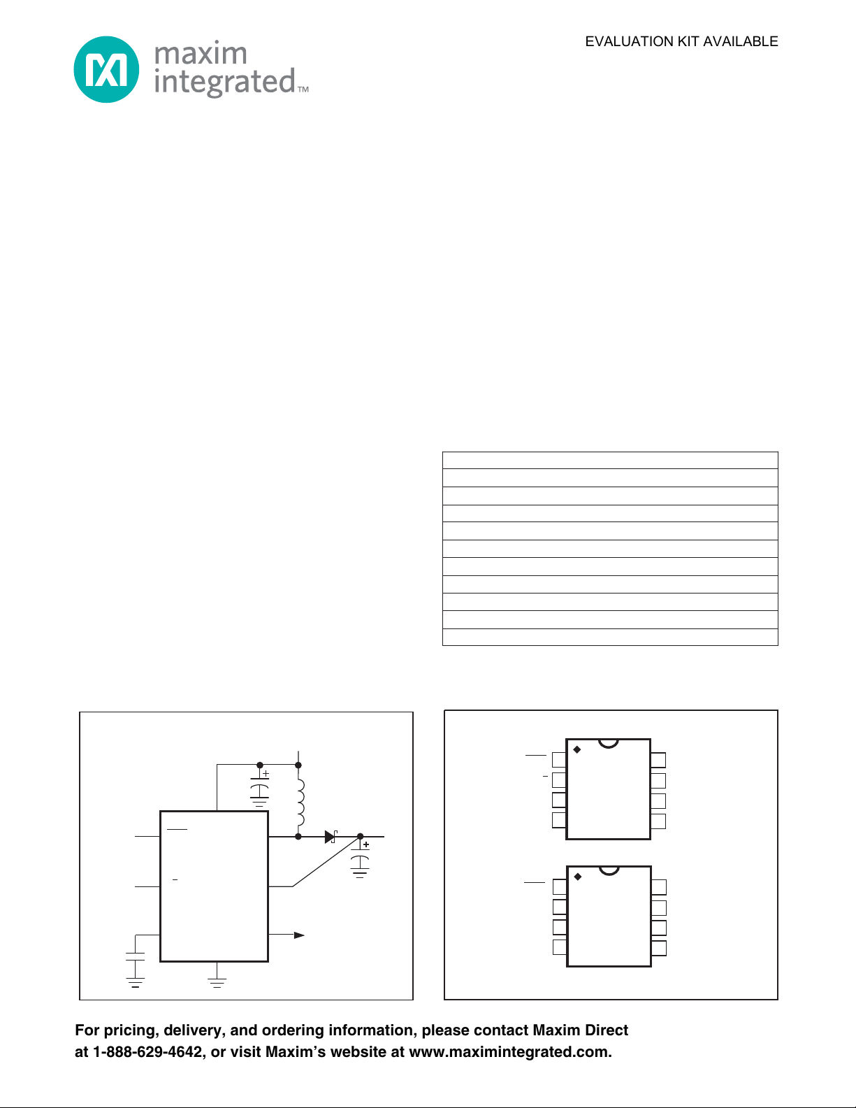
__________Typical Operating Circuit
INPUT
2V to V
OUT
150μF
8
6
4
22μH
1N5817
LOW-BATTERY
DETECTOR OUTPUT
5
1
SHDN
2
3/5
3
REF
0.1μF
LBI
LX
MAX756
OUT
LBO
GND
7
OUTPUT
5V at 200mA
or
3.3V at 300mA
100μF
_________________Pin Configurations
TOP VIEW
SHDN
SHDN
3/5
REF
LBO
REF
LBO
FB
1
2
3
4
1
2
3
4
MAX756
DIP/SO
MAX757
DIP/SO
8
LX
7
GND
6
OUT
5
LBI
8
LX
7
GND
6
OUT
5
LBI
19-0113; Rev. 2; 1/95

3.3V/5V/Adjustable-Output,
MAX756/MAX757
2
Maxim Integrated
Step-Up DC-DC Converters
ABSOLUTE MAXIMUM RATINGS
Supply Voltage (OUT to GND) ....................................-0.3V, +7V
Switch Voltage (LX to GND) ........................................-0.3V, +7V
Auxiliary Pin Voltages (SHDN
3/5
, FB to GND) ........................................-0.3V, (V
Reference Current (I
REF
Continuous Power Dissipation (T
, LBI, LBO, REF,
+ 0.3V)
OUT
) ....................................................2.5mA
= +70°C)
A
Plastic DIP (derate 9.09mW/°C above +70°C) .............727mW
SO (derate 5.88mW/°C above +70°C)..........................471mW
Stresses beyond those listed under “Absolute Maximum Ratings" may cause permanent damage to the device. These are stress ratings only, and functional
operation of the device at these or any other conditions beyond those indicated in the operational sections of the specifications is not implied. Exposure to
absolute maximum rating conditions for extended periods may affect device reliability.
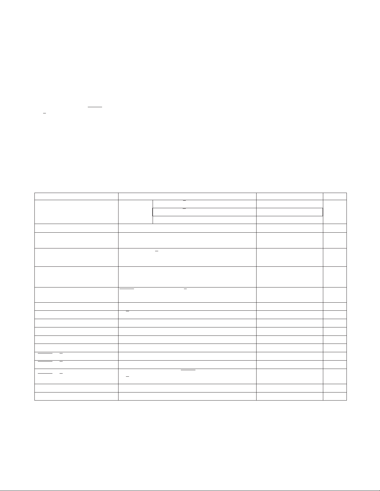
ELECTRICAL CHARACTERISTICS
(Circuits of Figure 1 and Typical Operating Circuit, VIN= 2.5V, I
MAX756, 3/5 = 0V, 0mA < I
Output Voltage
Minimum Start-Up Supply Voltage
Minimum Operating Supply
Voltage (once started)
Quiescent Supply Current in
3.3V Mode (Note 1)
2V < VIN< 3V
I
= 10mA
LOAD
I
= 20mA
LOAD
I
= 0mA, 3/5 = 3V, LBI = 1.25V, V
LOAD
FB = 1.3V (MAX757 only)
MAX756, 3/5 = 3V, 0mA < I
MAX757, V
Operating Temperature Ranges:
MAX75_C_ _ ........................................................0°C to +70°C
MAX75_E_ _......................................................-40°C to +85°C
Junction Temperature......................................................+150°C
Storage Temperature Range............................... -65°to +160°C
Lead Temperature (soldering, 10sec) ........................... +300°C
= 0mA, TA= T
LOAD
= 5V, 0mA < I
OUT
LOAD
LOAD
LOAD
to T
MIN
< 200mA
< 300mA
< 200mA
, unless otherwise noted.)
MAX
4.8 5.0 5.2
3.17 3.30 3.43 V
4.8 5.0 5.2
1.1 1.8
= 3.47V,
OUT
60
UNITSMIN TYP MAXCONDITIONSPARAMETER
V
V0.7
µA
Battery Quiescent Current
Measured at V
in Figure 1
IN
Shutdown Quiescent Current
(Note 1)
Reference Voltage
Reference-Voltage Regulation
LBO Output Voltage Low
SHDN = 0V, LBI = 1.25V, 3/5 = 3V, V
FB = 1.3V (MAX757 only)
= 0.1µF
REF
3/5 = 3V, -20µA < REF load < 250µA, C
I
= 2mA
SINK
OUT
= 3.47V,
= 0.22µF
REF
60Output set for 3.3V
LBO Output Leakage Current
SHDN, 3/5, FB, LBI Input Current
Output Voltage Range
LBI = 1.25V, FB = 1.25V, SHDN = 0V or 3V,
3/5 = 0V or 3V
MAX757, I
= 0mA (Note 2)
LOAD
Note 1: Supply current from the 3.3V output is measured with an ammeter between the 3.3V output and OUT pin. This current
correlates directly with actual battery supply current, but is reduced in value according to the step-up ratio and efficiency.
Note 2: Minimum value is production tested. Maximum value is guaranteed by design and is not production tested.
µA
µA20 40
V1.23 1.25 1.27No REF load, C
%0.8 2.0
V1.22 1.25 1.28With falling edgeLBI Input Threshold
mV25LBI Input Hysteresis
V0.4
µA1LBO = 5V
V0.4SHDN, 3/5 Input Voltage Low
V1.6SHDN, 3/5 Input Voltage High
nA±100
V1.22 1.25 1.28MAX757FB Voltage
V2.7 5.5

3.3V/5V/Adjustable-Output,
MAX756/MAX757
Maxim Integrated
3
Step-Up DC-DC Converters
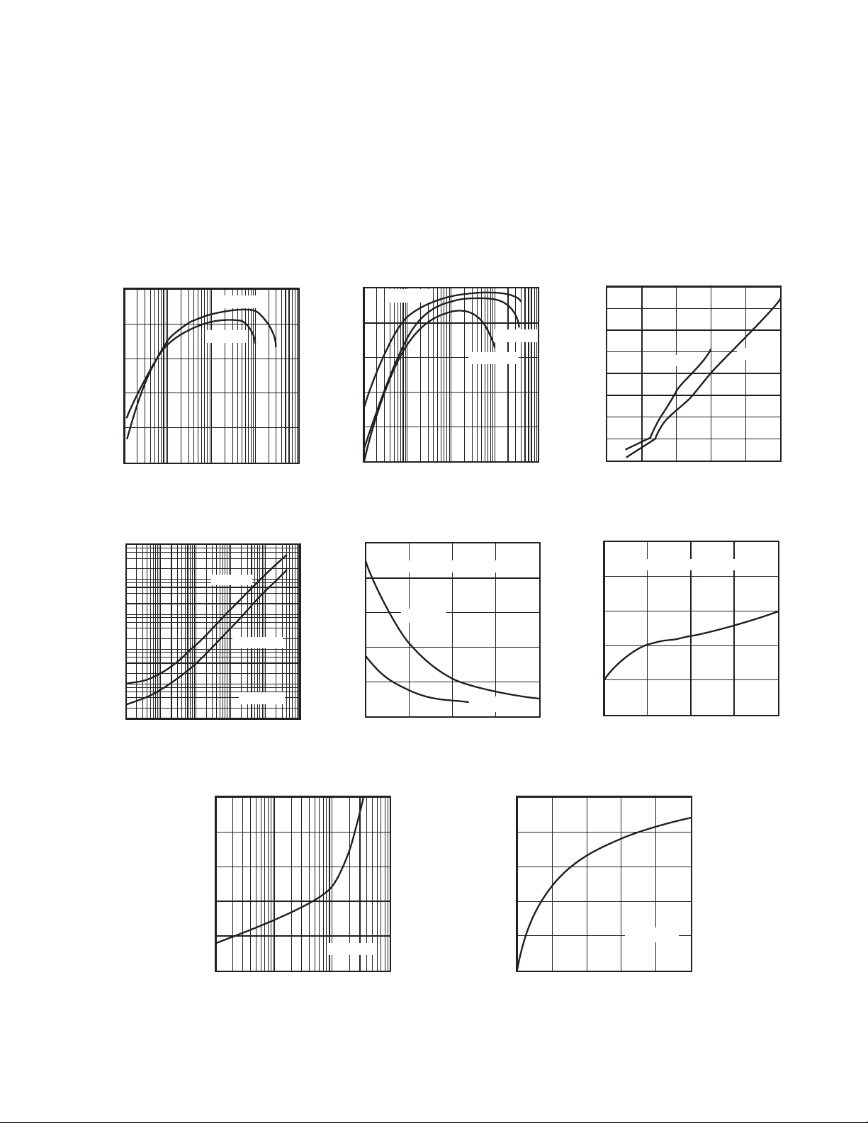
__________________________________________Typical Operating Characteristics
(Circuit of Figure 1, TA= +25°C, unless otherwise noted.)
EFFICIENCY vs. LOAD CURRENT
3.3V OUTPUT MODE
90
80
70
60
EFFICIENCY (%)
50
40
0.1 10 1000
1 100
LOAD CURRENT (mA)
VIN = 2.0V
VIN = 1.2V
SWITCHING FREQUENCY
vs. LOAD CURRENT
1M
100k
10k
1k
SWITCHING FREQUENCY (Hz)
100
10
10μ 10m 1
100μ 1m 100m
5V MODE
LOAD CURRENT (A)
3.3V MODE
VIN= 2.5V
MAX756-1
EFFICIENCY (%)
MAX756-4
QUIESCENT CURRENT (μA)
EFFICIENCY vs. LOAD CURRENT
5V OUTPUT MODE
90
80
70
60
50
40
VIN = 3.3V
VIN = 2.5V
VIN = 1.25V
0.1 10 1000
1 100
LOAD CURRENT (mA)
QUIESCENT CURRENT
vs. INPUT VOLTAGE
500
400
300
200
100
0
CURRENT MEASURED AT V
V
1
= 5V
OUT
2
3
INPUT VOLTAGE (V)
V
= 3.3V
OUT
4
MAXIMUM OUTPUT CURRENT
vs. INPUT VOLTAGE
800
MAX756-2
700
600
500
400
300
200
MAXIMUM OUTPUT CURRENT (mA)
100
0
02
3.3V MODE
13
INPUT VOLTAGE (V)
5V MODE
4
MAX756-3
5
SHUTDOWN QUIESCENT CURRENT
vs. INPUT VOLTAGE
50
IN
MAX756-5
40
30
20
10
SHUTDOWN QUIESCENT CURRENT (μA)
0
5
CURRENT MEASURED AT V
12 5
3
INPUT VOLTAGE (V)
IN
4
MAX756-6
MINIMUM START-UP INPUT VOLTAGE
1.8
1.6
1.4
1.2
START-UP INPUT VOLTAGE (V)
1.0
0.8
1
vs. LOAD CURRENT
3.3V MODE
10 100
LOAD CURRENT (mA)
1000
MAX756-7
REFERENCE VOLTAGE
LOAD REGULATION
10
8
6
4
VREF LOAD REGULATION (mV)
2
0
0
50 100 150 200
LOAD CURRENT (μA)
MAX756-8
V
= 3.3V
OUT
250
 Loading...