Page 1
General Description
The MAX7500–MAX7504 temperature sensors accurately measure temperature and provide an overtemperature alarm/interrupt/shutdown output. These
devices convert the temperature measurements to digital form using a high-resolution, sigma-delta, analog-todigital converter (ADC). Communication is through an
I2C-compatible 2-wire serial interface. The MAX7500/
MAX7501/MAX7502 integrate a timeout feature that
offers protection against I2C bus lockups. The
MAX7503/MAX7504 do not include the timeout feature.
The 2-wire serial interface accepts standard write byte,
read byte, send byte, and receive byte commands to
read the temperature data and configure the behavior
of the open-drain overtemperature shutdown output.
The MAX7500 features three address select lines, while
the MAX7501–MAX7504 feature two address select
lines and a RESET input. The MAX7500/MAX7501/
MAX7502s’ 3.0V to 5.5V supply voltage range, low
250µA supply current, and a lockup-protected I
2
C-compatible interface make them ideal for a wide range of
applications, including personal computers (PCs), electronic test equipment, and office electronics.
The MAX7500–MAX7504 are available in 8-pin µMAX
®
and SO packages and operate over the -55°C to
+125°C temperature range.
Applications
PCs
Servers
Office Electronics
Electronic Test Equipment
Industrial Process Control
Features
♦ Timeout Prevents Bus Lockup (MAX7500,
MAX7501, MAX7502)
♦ Hardware Reset for Added Protection
♦ I
2
C Bus Interface
♦ 3.0V to 5.5V Supply Voltage Range
♦ 250µA (typ) Operating Supply Current
♦ 3µA (typ) Shutdown Supply Current
♦ ±1.5°C (max) Temperature Accuracy (-25°C to
+100°C, 3-σ)
♦ µMAX, SO Packages Save Space
♦ Separate Open-Drain OS Output Operates as
Interrupt or Comparator/Thermostat Input
♦ Register Readback Capability
♦ Improved LM75 Second Source
MAX7500–MAX7504
Digital Temperature Sensors and Thermal
Watchdog with Bus Lockup Protection
________________________________________________________________
Maxim Integrated Products
1
Ordering Information/
Selector Guide
19-3382; Rev 4; 10/10
EVALUATION KIT
AVAILABLE
Ordering Information/Selector Guide continued at end of
data sheet.
Pin Configurations appear at end of data sheet.
µMAX is a registered trademark of Maxim Integrated Products, Inc.
For pricing, delivery, and ordering information, please contact Maxim Direct at 1-888-629-4642,
or visit Maxim's website at www.maxim-ic.com.
Typical Application Circuits
PART
MAX7500MSA
TEMP
RANGE
-55°C to
+125°C
PINPACKAGE
8 SO X X
RESET TIMEOUT
+3.0V TO +5.5V+3.0V TO +5.5V
TO I
4.7kΩ
2
C MASTER
SDA
SCL
GND
+V
S
A0
MAX7501
OS
MAX7502
MAX7503
MAX7504
A1
RESET
4.7kΩ
+V
SDA
TO I2C MASTER
SCL
GND
OS
MAX7500
S
A0
A1
A2
Page 2

MAX7500–MAX7504
Digital Temperature Sensors and Thermal
Watchdog with Bus Lockup Protection
2 _______________________________________________________________________________________
ABSOLUTE MAXIMUM RATINGS
ELECTRICAL CHARACTERISTICS
(+VS = +3.0V to +5.5V, TA= -55°C to +125°C, unless otherwise noted. Typical values are at +VS= +3.3V, TA= +25°C.) (Notes 4, 5)
Stresses beyond those listed under “Absolute Maximum Ratings” may cause permanent damage to the device. These are stress ratings only, and functional
operation of the device at these or any other conditions beyond those indicated in the operational sections of the specifications is not implied. Exposure to
absolute maximum rating conditions for extended periods may affect device reliability.
Note 1: Absolute Maximum Ratings indicate limits beyond which damage to the device may occur. DC and AC electrical specifica-
tions do not apply when operating the device beyond its rated operating conditions.
Note 2: When the input voltage (V
I
) at any pin exceeds the power supplies (VI< V
GND
or VI> + VS), the current at that pin should be
limited to 5mA. The 20mA maximum package input current rating limits the number of pins that can safely exceed the power
supplies with an input current of 5mA to 4.
Note 3: Human Body Model, 100pF discharged through a 1.5kΩ resistor.
(Note 1)
+V
S
to GND ............................................................. -0.3V to +6V
OS, SDA, SCL to GND.......................................... -0.3V to +6.0V
All Other Pins to GND................................ -0.3V to (+V
S
+ 0.3V)
Input Current at Any Pin (Note 2) ..................................... +5mA
Package Input Current (Note 2) ..................................... +20mA
ESD Protection (all pins, Human Body Model, Note 3)... ±2000V
Continuous Power Dissipation (T
A
= +70°C)
8-Pin µMAX (derate 4.5mW/°C above +70°C) ............ 362mW
8-Pin SO (derate 5.9mW/°C above +70°C)................. 471mW
Operating Temperature Range ....................... -55°C to +125°C
Junction Temperature .................................................... +150°C
Storage Temperature Range ........................... -65°C to +150°C
Lead Temperature (soldering, 10s) ............................... +300°C
Soldering Temperature (reflow)
Lead(Pb)-free.............................................................. +260°C
Containing lead(Pb) .................................................... +240°C
Accuracy, 6-σ
Accuracy, 3-σ (Note 5)
Resolution 9 bits
Conversion Time (Note 6) 100 ms
+VS Supply Voltage Range 3.0 5.5 V
OS Output Saturation Voltage I
OS Delay (Note 8) 1 6
TOS Default Temperature (Note 9) 80 °C
T
HYST
LOGIC (SDA, SCL, A0, A1, A2)
Input High Voltage V
Input Low Voltage V
Input High Current I
Input Low Current I
Input Capacitance All digital inputs 5 pF
Output High Current VIN = 5V 1 µA
Output Low Voltage IOL = 3mA 0.4 V
PARAMETER SYMBOL CONDITIONS MIN TYP MAX UNITS
-25°C ≤ TA ≤ +100°C -2.0 ±2.0
-55°C ≤ T
-25°C ≤ TA ≤ +100°C -1.5 +1.5
-55°C ≤ T
I2C inactive 0.25 0.5 mA
Shutdown mode, +VS = 3V 3Quiescent Supply Current
Shutdown mode, +V
OUT
Default Temperature (Note 9) 75 °C
IH
IL
IH
IL
VIN = 5V 0.005 1.0 µA
VIN = 0V 0.005 1.0 µA
A
A
= 4.0mA (Note 7) 0.8 V
≤ +125°C -3.0 ±3.0
≤ +125°C -2.0 +2.0
= 5V 5
S
+VS x
0.7
+VS x
0.3
°C
°C
µA
Conver-
sions
V
V
Page 3

MAX7500–MAX7504
Digital Temperature Sensors and Thermal
Watchdog with Bus Lockup Protection
_______________________________________________________________________________________ 3
Note 4: All parameters are measured at +25°C. Values over the temperature range are guaranteed by design.
Note 5: There are no industry-wide standards for temperature accuracy specifications. These values allow comparison to ven-
dors who use 3-σ limits.
Note 6: This specification indicates how often temperature data is updated. The devices can be read at any time without regard
to conversion state, while yielding the last conversion result.
Note 7: For best accuracy, minimize output loading. Higher sink currents can affect sensor accuracy due to internal heating.
Note 8: OS delay is user programmable up to six “over-limit” conversions before OS is set to minimize false tripping in noisy
environments.
Note 9: Default values set at power-up.
Note 10: All timing specifications are guaranteed by design.
Note 11: A master device must provide a hold time of at least 300ns for the SDA signal to bridge the undefined region of SCL’s
falling edge.
Note 12: C
B
= total capacitance of one bus line in pF. Tested with CB= 400pF.
Note 13: Input filters on SDA, SCL, and A_ suppress noise spikes less than 50ns.
Note 14: Holding the SDA line low for a time greater than t
TIMEOUT
causes the devices to reset SDA to the IDLE state of the serial
bus communication (SDA set high).
ELECTRICAL CHARACTERISTICS (continued)
(+VS = +3.0V to +5.5V, TA= -55°C to +125°C, unless otherwise noted. Typical values are at +VS= +5V, TA= +25°C.) (Notes 4, 5)
PARAMETER SYMBOL CONDITIONS MIN TYP MAX UNITS
I2C-COMPATIBLE TIMING (Note 10)
Serial Clock Frequency f
Minimum RESET Pulse Width 1 µs
Bus Free Time Between STOP
and START Conditions
START Condition Hold Time t
STOP Condition Setup Time t
Clock Low Period t
Clock High Period t
START Condition Setup Time t
Data Setup Time t
Data Hold Time t
Maximum Receive SCL/SDA Rise
Time
Minimum Receive SCL/SDA Rise
Time
Maximum Receive SCL/SDA Fall
Time
Minimum Receive SCL/SDA Fall
Time
Transmit SDA Fall Time t
Pulse Width of Suppressed Spike t
SDA Time Low for Reset of Serial
Interface
SCL
t
BUF
HD:STA
SU:STO
LOW
HIGH
SU:STA
SU:DAT
HD:DAT
t
t
t
t
SP
t
TIMEOUT
Bus timeout inactive DC 400 kHz
1.3 µs
0.6 µs
90% of SCL to 10% of SDA 100 ns
1.3 µs
0.6 µs
90% of SCL to 90% of SDA 100 ns
10% of SDA to 10% of SCL 100 ns
10% of SCL to 10% of SDA (Note 11) 0 0.9 µs
R
(Note 12)
R
F
(Note 12)
F
20 +
(Note 12)
F
(Note 13) 0 50 ns
MAX7500/MAX7501/MAX7502 (Note 14) 150 300 ms
0.1 x
C
300 ns
20 +
0.1 x
C
B
300 ns
20 +
0.1 x
C
B
B
250 ns
ns
ns
Page 4
MAX7500–MAX7504
Digital Temperature Sensors and Thermal
Watchdog with Bus Lockup Protection
4 _______________________________________________________________________________________
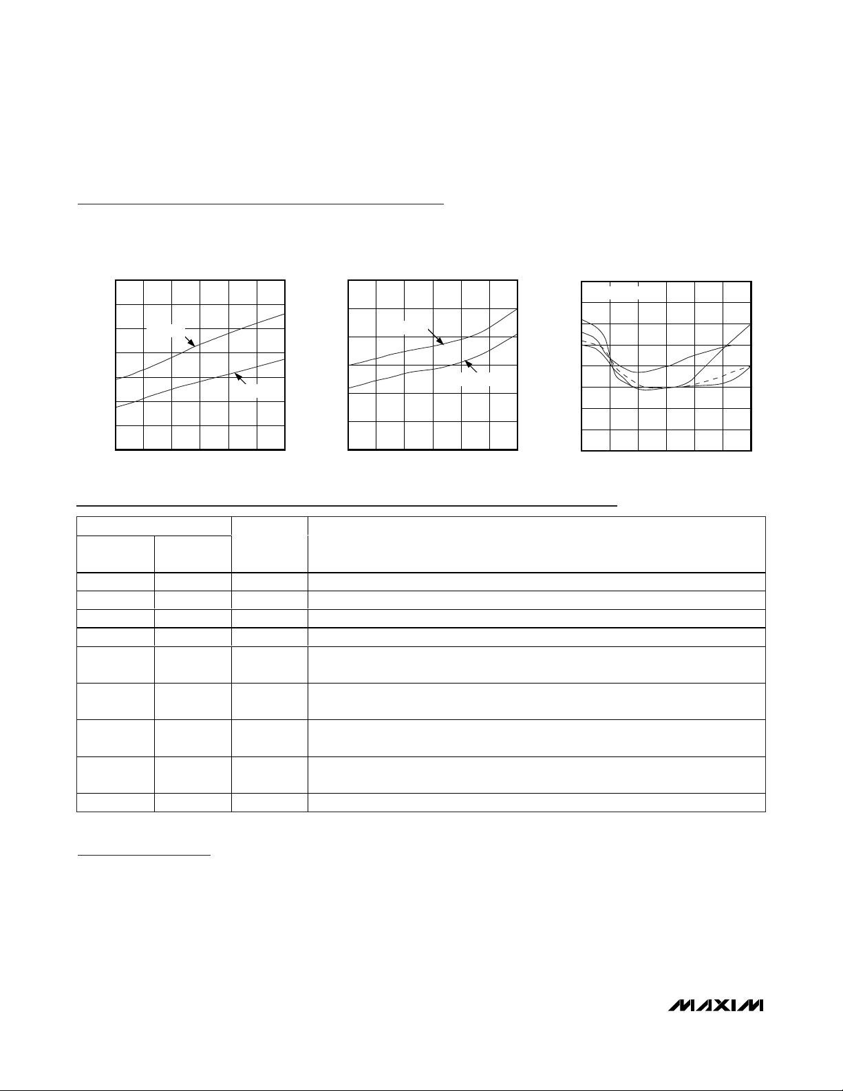
Typical Operating Characteristics
(TA = +25°C, unless otherwise noted.)
QUIESCENT SUPPLY CURRENT
vs. TEMPERATURE
MAX7500 toc01
TEMPERATURE (°C)
QUIESCENT SUPPLY CURRENT (μA)
9565355-25
240
250
260
270
280
290
300
230
-55 125
+VS = +5V
+VS = +3V
SHUTDOWN SUPPLY CURRENT (μA)
1
2
3
4
5
6
0
SHUTDOWN SUPPLY CURRENT
vs. TEMPERATURE
MAX7500 toc02
TEMPERATURE (°C)
9565355-25-55 125
+VS = +5V
+VS = +3V
ACCURACY vs. TEMPERATURE
ACCURACY (°C)
-1.5
-1.0
-0.5
0
0.5
1.0
1.5
2.0
-2.0
MAX7500 toc03
TEMPERATURE (°C)
9565355-25-55 125
4 TYPICAL PARTS
Pin Description
Detailed Description
The MAX7500–MAX7504 temperature sensors measure
temperature, convert the data into digital form using a
sigma-delta ADC, and communicate the conversion
results through an I2C-compatible 2-wire serial interface. These devices accept standard I2C commands to
read the data, set the overtemperature alarm (OS) trip
thresholds, and configure other characteristics. The
MAX7500 features three address select lines (A0, A1,
A2) while the MAX7501–MAX7504 feature two address
select lines (A0, A1) and a RESET input. The
MAX7500–MAX7504 operate from +3.0V to +5.5V supply voltages and consume 250µA of supply current.
PIN
MAX7500
MAX7501–
MAX7504
1 1 SDA Serial Data Input/Output Line. Open drain. Connect SDA to a pullup resistor.
2 2 SCL Serial Data Clock Input. Open drain. Connect SCL to a pullup resistor.
3 3 OS Overtemperature Shutdown Output. Open drain. Connect OS to a pullup resistor.
4 4 GND Ground
5—A2
—5RESET
66A1
77A0
88+V
NAME FUNCTION
2-Wire Interface Address Input. Connect A2 to GND or +V
address. Do not leave unconnected (see Table 1).
Active-Low Reset Input. Pull RESET low for longer than the minimum reset pulse width
2
to reset the I
C bus and all internal registers to their POR values.
2-Wire Interface Address Input. Connect A1 to GND or +V
address. Do not leave unconnected (see Table 1).
2-Wire Interface Address Input. Connect A0 to GND or +V
address. Do not leave unconnected (see Table 1).
Positive Supply Voltage Input. Bypass to GND with a 0.1µF bypass capacitor.
S
to set the desired I2C bus
S
to set the desired I2C bus
S
to set the desired I2C bus
S
Page 5
MAX7500–MAX7504
Digital Temperature Sensors and Thermal
Watchdog with Bus Lockup Protection
_______________________________________________________________________________________ 5
I2C-Compatible Bus Interface
From a software perspective, the MAX7500–MAX7504
appear as a set of byte-wide registers that contain temperature data, alarm threshold values, and control bits.
A standard I2C-compatible 2-wire serial interface reads
temperature data and writes control bits and alarm
threshold data. Each device responds to its own I2C
slave address, which is selected using A0, A1, and A2.
See Table 1.
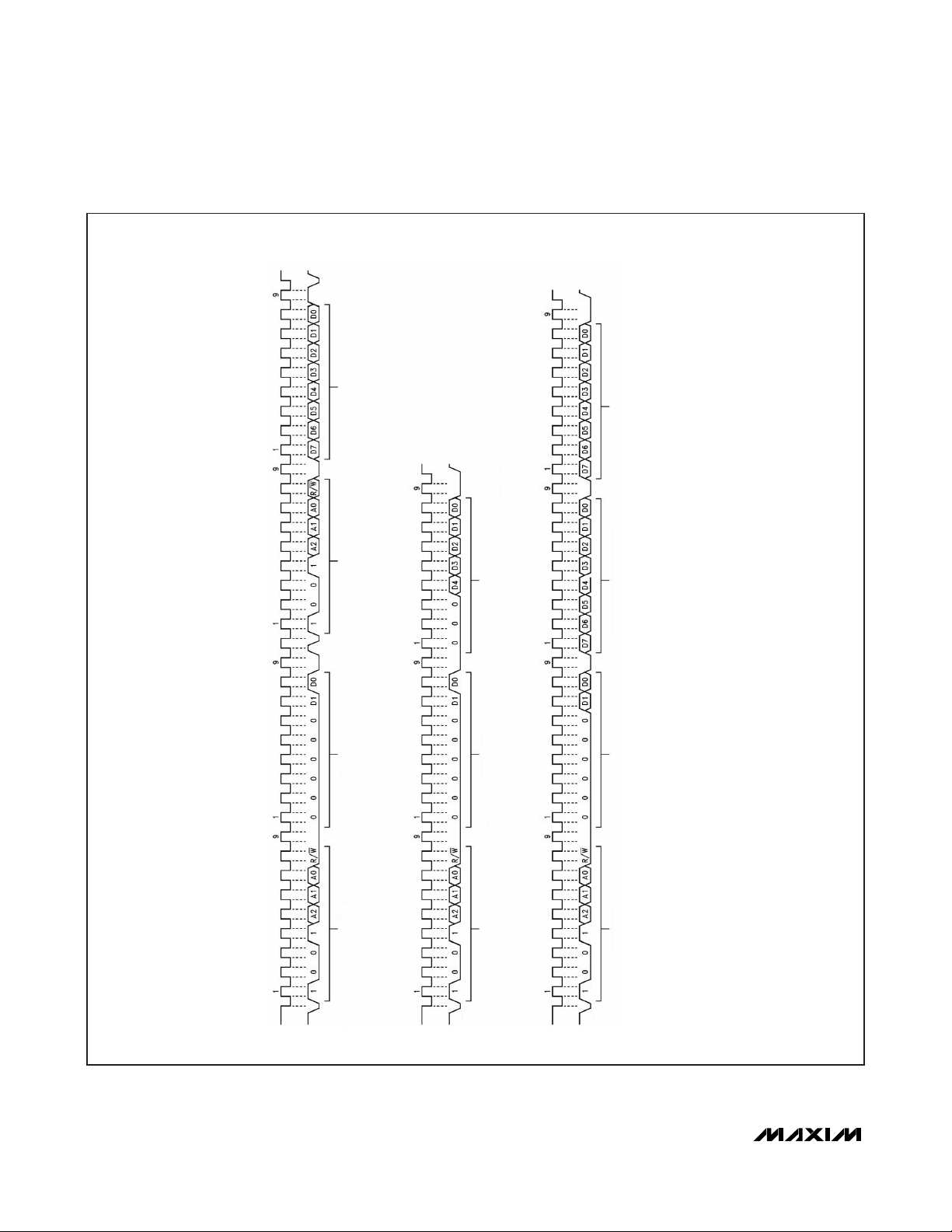
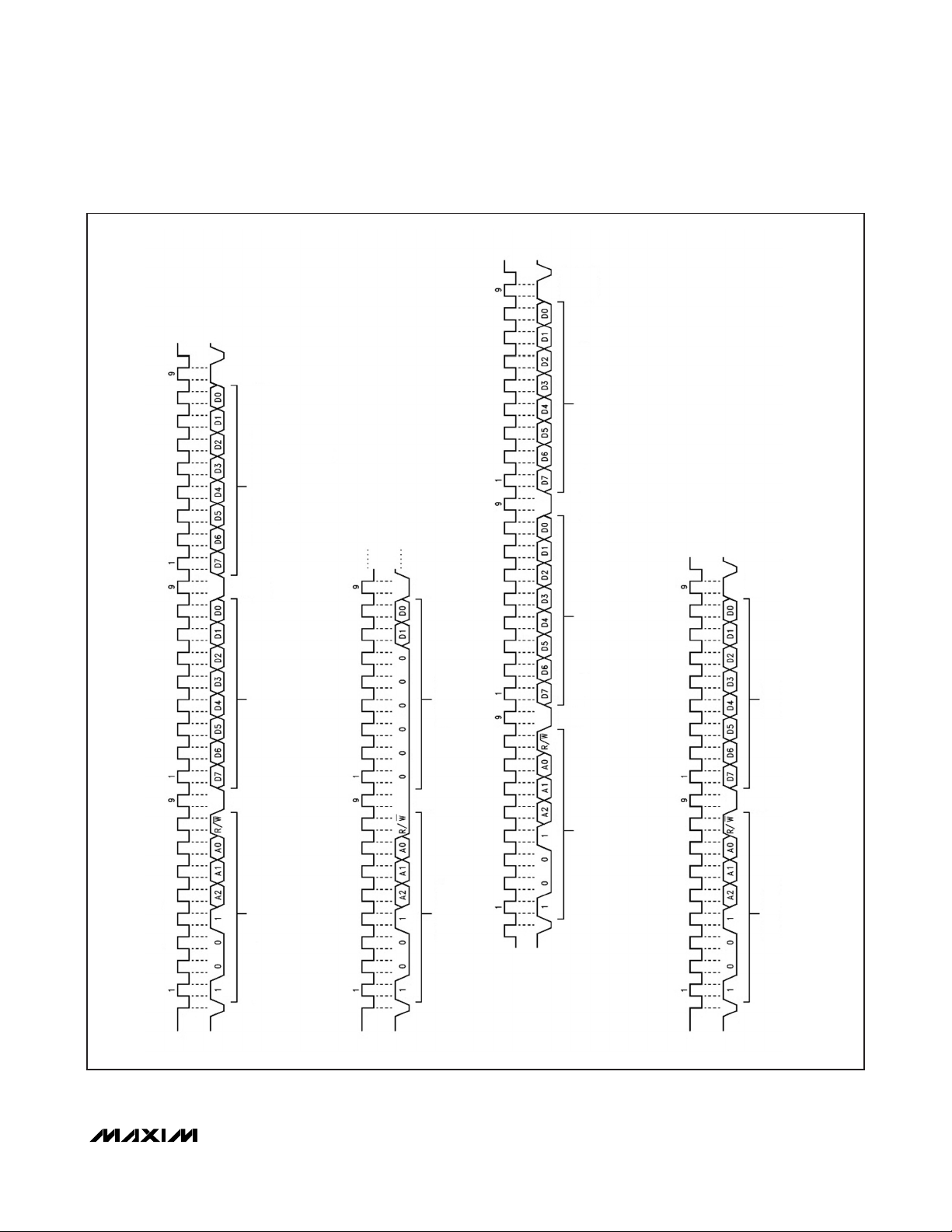
The MAX7500–MAX7504 employ four standard I2C
protocols: write byte, read byte, send byte, and receive
byte (Figures 1, 2, and 3). The shorter receive byte protocol allows quicker transfers, provided that the correct
data register was previously selected by a read-byte
instruction. Use caution when using the shorter protocols in multimaster systems, as a second master could
overwrite the command byte without informing the first
master. The MAX7500 has eight different slave
addresses available; therefore, a maximum of eight
MAX7500 devices can share the same bus. The
MAX7501–MAX7504 each have four different slave
addresses available.
Table 1. I2C Slave Addresses
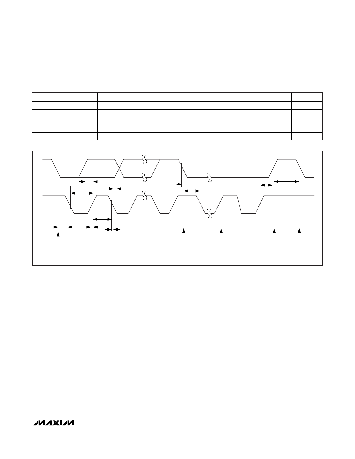
Figure 1. Serial Bus Timing
DEVICE BIT 7 BIT 6 BIT 5 BIT 4 BIT 3 BIT 2 BIT 1 BIT 0
MAX7500 1 0 0 1 A2 A1 A0 RD/W
MAX7501 1 0 0 1 1 A1 A0 RD/W
MAX7502 1 0 0 1 0 A1 A0 RD/W
MAX7503 1 0 0 1 1 A1 A0 RD/W
MAX7504 1 0 0 1 0 A1 A0 RD/W
SDA
t
STOP
(P)
BUF
START
CONDITION
(S)
t
SU:DAT
t
LOW
SCL
t
HIGH
t
HD:STA
t
R
START
CONDITION
(S)
PARAMETERS ARE MEASURED FROM 10% TO 90%.
t
t
HD:DAT
t
F
SU:STA
REPEATED START
CONDITION
(SR)
t
HD:STA
ACKNOWLEDGE
(A)
t
SU:STO
CONDITION
Page 6
MAX7500–MAX7504
Digital Temperature Sensors and Thermal
Watchdog with Bus Lockup Protection
6 _______________________________________________________________________________________
Figure 2. I2C-Compatible Timing Diagram (Write)
STOP
MASTER
COND BY
NO
ACK BY
ACK BY
MASTER
BYTE
DATA
MAX7504
MAX7500–
STOP
MASTER
COND BY
ACK BY
MAX7504
MAX7500–
STOP
COND BY
MASTER
ACK BY
MAX7504
MAX7500–
DATA BYTE
LEAST-SIGNIFICANT
ACK BY
MAX7504
MAX7500–
BYTE
ADDRESS
START
REPEAT
ACK BY
MAX7500–
BY
MASTER
MAX7504
BYTE
CONFIGURATION
ACK BY
MAX7504
MAX7500–
DATA BYTE
MOST-SIGNIFICANT
ACK BY
MAX7504
MAX7500–
(b) CONFIGURATION REGISTER WRITE
WRITE
LOW
AND T
HIGH
(c) T
ACK BY
START
BYTE
POINTER
MAX7504
MAX7500–
BYTE
ADDRESS
BY
MASTER
BYTE
POINTER
(a) TYPICAL POINTER SET FOLLOWED BY IMMEDIATE READ FROM CONFIGURATION REGISTER
ACK BY
MAX7504
MAX7500–
BYTE
ADDRESS
BY
START
MASTER
BY
START
BYTE
POINTER
ACK BY
MAX7500–
BYTE
ADDRESS
MASTER
MAX7504
Page 7
MAX7500–MAX7504
Digital Temperature Sensors and Thermal
Watchdog with Bus Lockup Protection
_______________________________________________________________________________________ 7
Figure 3. I2C-Compatible Timing Diagram (Read)
STOP
MASTER
COND BY
NO
ACK BY
MASTER
STOP
MASTER
COND BY
MASTER
NO ACK BY
DATA BYTE
LEAST-SIGNIFICANT
.
LOW
MASTER
, T
HIGH
STOP
MASTER
COND BY
NO
ACK BY
MASTER
.
LOW
DATA BYTE
, T
HIGH
LEAST-SIGNIFICANT
ACK BY
MASTER
ACK BY
MAX7500–
ACK BY
MAX7504
DATA BYTE
MOST-SIGNIFICANT
ACK BY
MAX7504
MAX7500–
BYTE
ADDRESS
BY
START
MASTER
POINTER BYTE
(a) TYPICAL 2-BYTE READ FROM PRESET POINTER LOCATION SUCH AS TEMP, T
ACK BY
MASTER
ADDRESS BYTE
BY
START
MASTER
START
REPEAT
DATA BYTE
MOST-SIGNIFICANT
ACK BY
MAX7504
MAX7500–
(b) TYPICAL POINTER SET FOLLOWED BY IMMEDIATE READ FOR 2-BYTE REGISTER SUCH AS TEMP, T
BYTE
ADDRESS
BY
MASTER
START
ACK BY
BY
BYTE
DATA
(c) TYPICAL 1-BYTE READ FROM CONFIGURATION REGISTER WITH PRESET POINTER.
MAX7504
MAX7500–
BYTE
ADDRESS
MASTER
Page 8

MAX7500–MAX7504
Register Descriptions
The MAX7500–MAX7504 have an internal pnp-junctionbased temperature sensor whose analog output is converted to digital form using a 9-bit sigma-delta ADC.
The measured temperature and temperature configurations are controlled by the temperature, configuration,
T
HYST
, and TOSregisters. See Table 2.
Temperature Register
Read the measured temperature through the temperature register. The temperature data format is 9 bits,
two’s complement, and the register is read out in 2
bytes: an upper byte and a lower byte. Bit D15 is the
sign bit. When bit D15 is 1, the temperature reading is
negative. When bit D15 is zero, the temperature reading is positive. Bits D14–D7 contain the temperature
data, with the LSB representing 0.5°C and the MSB
representing 64°C (see Table 3). The MSB is transmitted first. The last 7 bits of the lower byte, bits D6–D0,
are don’t cares. When reading the temperature register,
bits D6–D0 must be ignored. When the measured temperature is greater than +127.5°C, the value stored in
the temperature register is clipped to 7F8h. When the
measured temperature is below -64°C, the value in the
temperature register is clipped to BF8h.
During the time of reading the temperature register, any
changes in temperature are ignored until the read is
completed. The temperature register is updated upon
completion of the next conversion.
Table 3 lists the temperature register definition.
Configuration Register
The 8-bit configuration register sets the fault queue, OS
polarity, shutdown control, and whether the OS output
functions in comparator or interrupt mode. When writing
to the configuration register, set bits D7, D6, and D5 to
zero. See Table 5.
Bits D4 and D3, the fault queue bits, determine the
number of faults necessary to trigger an OS condition.
See Table 6. The number of faults set in the queue must
occur to trip the OS output. The fault queue prevents
OS false tripping in noisy environments.
Set bit D2, the OS polarity bit, to zero to force the OS
output active low. Set bit D2 to 1 to set the OS output
polarity to active high. OS is an open-drain output
under all conditions and requires a pullup resistor to
output a high voltage. See Figure 4.
Set bit D1, the comparator/interrupt bit to zero to run
the overtemperature shutdown block in comparator
mode. In comparator mode, OS is asserted when the
temperature rises above the TOSvalue. OS is deasserted when the temperature drops below the T
HYST
value.
Digital Temperature Sensors and Thermal
Watchdog with Bus Lockup Protection
8 _______________________________________________________________________________________
Table 2. Register Functions
Table 3. Temperature Register Definition
Table 4. Temperature Data Output
X = Don’t care.
REGISTER NAME ADDRESS (HEX) POR STATE (HEX)
Temperature 00 — — — Read only
Configuration 01 00 0000 0000 — R/W
T
HYST
T
OS
02 4B0 0100 1011 0 75 R/W
03 500 0101 0000 0 80 R/W
UPPER BYTE LOWER BYTE
D15 D14 D13 D12 D11 D10 D9 D8 D7 D6 D5 D4 D3 D2 D1 D0
Sign bit
1= Negative
0 = Positive
MSB
64°C
32°C16°C8°C4°C2°C1°C
TEMPERATURE (°C)
+125 0111 1101 0xxx xxxx 7D0x
+25 0001 1001 0xxx xxxx 190x
+0.5 0000 0000 1xxx xxxx 008x
0 0000 0000 0xxx xxxx 000x
-0.5 1111 1111 1xxx xxxx FF8x
-25 1110 0111 0xxx xxxx E70x
-55 1100 1001 0xxx xxxx C90x
DIGITAL OUTPUT
BINARY hex
POR STATE
(BINARY)
LSB
0.5°C
POR STATE (°C)
XXXXXXX
READ/
WRITE
Page 9

See Figure 4. Set bit D1 to 1 to run the overtemperature
shutdown block in interrupt mode. OS is asserted in
interrupt mode when the temperature rises above the
TOSvalue or falls below the T
HYST
value. OS is
deasserted only after performing a read operation.
Set bit D0, the shutdown bit, to zero for normal operation. Set bit D0 to 1 to shut down the MAX7500–
MAX7504 internal blocks, dropping the supply current
to 3µA. The I2C interface remains active as long as the
shutdown bit is set. The TOS, T
HYST
, and configuration
registers can still be written to and read from while in
shutdown.
TOSand T
HYST
Registers
In comparator mode, the OS output behaves like a thermostat. The output asserts when the temperature rises
above the limit set in the TOSregister. The output
deasserts when the temperature falls below the limit set
in the T
HYST
register. In comparator mode, the OS output
can be used to turn on a cooling fan, initiate an emergency shutdown signal, or reduce system clock speed.
In interrupt mode, exceeding T
OS
also asserts OS. OS
remains asserted until a read operation is performed on
any of the registers. Once OS has asserted due to
crossing above TOSand is then reset, it is asserted
again only when the temperature drops below T
HYST
.
The output remains asserted until it is reset by a read.
Putting the MAX7500–MAX7504 into shutdown mode
also resets OS.
The TOSand T
HYST
registers are accessed with 2
bytes, with bits D15–D7 containing the data. Bits
D6–D0 are don’t cares when writing to these two registers and read-back zeros when reading from these registers. The LSB represents 0.5°C while the MSB
represents 64°C. See Table 7.
MAX7500–MAX7504
Digital Temperature Sensors and Thermal
Watchdog with Bus Lockup Protection
_______________________________________________________________________________________ 9
Table 5. Configuration Register Definition
Table 6. Configuration Register Fault
Queue Bits
Figure 4. OS Timing Diagram
Table 7. TOSand T
HYST
Register Definitions
X = Don’t care.
D7 D6 D5 D4 D3 D2 D1 D0
0 0 0 Fault queue Fault queue OS polarity
D4 D3 NO. OF FAULTS
0 0 1 (POR state)
01 2
10 4
11 6
Comparator/
T
OS
TEMPERATURE
T
HYST
OS OUTPUT
(COMPARATOR MODE)
OS SET ACTIVE LOW
OS OUTPUT
(INTERRUPT MODE)
OS SET ACTIVE LOW
READ
OPERATION
interrupt
READ
OPERATION
Shutdown
READ
OPERATION
COMMAND
Write
Read
D15 D14 D13 D12 D11 D10 D9 D8 D7 D6 D5 D4 D3 D2 D1 D0
Sign bit
1 = negative
0 = positive
Sign bit
1 = negative
0 = positive
MSB
64°C
MSB
64°C
UPPER BYTE LOWER BYTE
32°C16°C8°C4°C2°C1°C
32°C16°C8°C4°C2°C1°C
LSB
0.5°C
LSB
0.5°C
XXXX X XX
0000 0 00
Page 10

MAX7500–MAX7504
Shutdown
Set bit D0 in the configuration register to 1 to place the
MAX7500–MAX7504 in shutdown mode and reduce
supply current to 3µA.
Power-Up and Power-Down
The MAX7500–MAX7504 power up to a known state, as
indicated in Table 2. Some of these settings are summarized below:
• Comparator mode
•TOS= +80°C
•T
HYST
= +75°C
• OS active low
• Pointer = 00
Internal Registers
The MAX7500–MAX7504s’ pointer register selects
between four data registers. See Figure 5. At power-up,
the pointer is set to read the temperature register at
address 00. The pointer register latches the last location to which it was set. All registers are read and write,
except the temperature register, which is read only.
Write to the configuration register by writing an address
byte, a data pointer byte, and a data byte. If 2 data
bytes are written, the second data byte overrides the
first. If more than 2 data bytes are written, only the first
2 bytes are recognized while the remaining bytes are
ignored. The TOSand T
HYST
registers require 1
address byte and 1 pointer byte and 2 data bytes. If
only 1 data byte is written, it is saved in bits D15–D8 of
the respective register. If more than 2 data bytes are
written, only the first 2 bytes are recognized while the
remaining bytes are ignored.
Read from the MAX7500–MAX7504 in one of two ways.
If the location latched in the pointer register is set from
the previous read, the new read consists of an address
byte, followed by retrieving the corresponding number
of data bytes. If the pointer register needs to be set to a
new address, perform a read operation by writing an
address byte, pointer byte, repeat start, and another
address byte.
An inadvertent 8-bit read from a 16-bit register, with the
D7 bit low, can cause the MAX7500–MAX7504 to stop
in a state where the SDA line is held low. Ordinarily, this
would prevent any further bus communication until the
master sends nine additional clock cycles or SDA goes
high. At that time, a stop condition resets the device.
With the MAX7500/MAX7501/MAX7502, if the additional
clock cycles are not generated by the master, the bus
resets and unlocks after the bus timeout period has
elapsed.
The MAX750–MAX7504 can be reset by pulsing RESET
low.
Bus Timeout
Communication errors sometimes occur due to noise
pickup on the bus. In the worst case, such errors can
cause the slave device to hold the data line low, thereby preventing other devices from communicating over
the bus. The MAX7500/MAX7501/MAX7502s’ internal
bus timeout circuit resets the bus and releases the data
line if the line is low for more than 250ms. When the bus
timeout is active, the minimum serial clock frequency is
limited to 6Hz.
RESET
The RESET input on the MAX7503/MAX7504 provides a
way to reset the I2C bus and all the internal registers to
their initial POR values. To reset, apply a low pulse with
a duration of at least 1µs to the RESET input.
Digital Temperature Sensors and Thermal
Watchdog with Bus Lockup Protection
10 ______________________________________________________________________________________
Figure 5. Block Diagram
+V
SET POINT
OS
DATA
S
SMBus
INTERFACE
BLOCK
ADDRESS
POINTER REGISTER
(SELECTS REGISTER
FOR COMMUNICATION)
REGISTER SELECT
GND
A0
A1
A2/RESET
SDA
SCL
TEMPERATURE
(READ ONLY)
POINTER = 0000 0000
T
(READ/WRITE)
POINTER = 0000 0011
MAX7504
CONFIGURATION
(READ/WRITE)
POINTER = 0000 0001
SET POINT
T
HYST
(READ/WRITE)
POINTER = 0000 0010
OS
Page 11
Applications Information
Digital Noise
The MAX7500–MAX7504 feature an integrated lowpass
filter on both the SCL and the SDA digital lines to mitigate the effects of bus noise. Although this filtering
makes communication robust in noisy environments,
good layout practices are always recommended.
Minimize noise coupling by keeping digital traces away
from switching power supplies. Ensure that digital lines
containing high-speed data communications cross at
right angles to the SDA and SCL lines.
Excessive noise coupling into the SDA and SCL lines
on the MAX7500–MAX7504—specifically noise with
amplitude greater than 400mV
P-P
(the MAX7500–
MAX7504s’ typical hysteresis), overshoot greater than
300mV above +V
S
, and undershoot more than 300mV
below GND—may prevent successful serial communication. Serial bus no-acknowledge is the most common
symptom, causing unnecessary traffic on the bus.
Care must be taken to ensure proper termination within
a system with long PCB traces or multiple parts on the
bus. Resistance can be added in series with the SDA
and SCL lines to further help filter noise and ringing. If it
proves to be necessary, a 5kΩ resistor should be
placed in series with the SCL line, placed as close as
possible to SCL. This 5kΩ resistor, with the 5pF to 10pF
stray capacitance of the MAX7500–MAX7504 provide a
6MHz to 12MHz lowpass filter, which is sufficient filtering in most cases.
Chip Information
PROCESS: CMOS
MAX7500–MAX7504
Digital Temperature Sensors and Thermal
Watchdog with Bus Lockup Protection
______________________________________________________________________________________ 11
Ordering Information/
Selector Guide (continued)
+
Denotes a lead(Pb)-free/RoHS-compliant package.
1
2
3
4
8
7
6
5
+V
S
A0
A1
A2GND
OS
SCL
SDA
MAX7500
μMAX, SO
1
2
3
4
8
7
6
5
+V
S
A0
A1
RESETGND
OS
SCL
SDA
MAX7501–
MAX7504
μMAX, SO
TOP VIEW
Pin Configurations
PART
MAX7500MSA+
MAX7500MUA
MAX7500MUA+
MAX7501MSA
MAX7501MSA+
MAX7501MUA
MAX7501MUA+
MAX7502MSA
MAX7502MSA+
MAX7502MUA
MAX7502MUA+
MAX7503MSA
MAX7503MSA+
MAX7503MUA
MAX7503MUA+
MAX7504MSA
MAX7504MSA+
MAX7504MUA
MAX7504MUA+
TEMP
RANGE
-55°C to
+125°C
-55°C to
+125°C
-55°C to
+125°C
-55°C to
+125°C
-55°C to
+125°C
-55°C to
+125°C
-55°C to
+125°C
-55°C to
+125°C
-55°C to
+125°C
-55°C to
+125°C
-55°C to
+125°C
-55°C to
+125°C
-55°C to
+125°C
-55°C to
+125°C
-55°C to
+125°C
-55°C to
+125°C
-55°C to
+125°C
-55°C to
+125°C
-55°C to
+125°C
PINPACKAGE
8 SO X X
8 µMAX X X
8 µMAX X X
8 SO X X
8 SO X X
8 µMAX X X
8 µMAX X X
8 SO X —
8 SO X —
8 µMAX X —
8 µMAX X —
8 SO X —
8 SO X —
8 µMAX X —
8 µMAX X —
8 SO X —
8 SO X —
8 µMAX X —
8 µMAX X —
RESET TIMEOUT
Page 12

MAX7500–MAX7504
Digital Temperature Sensors and Thermal
Watchdog with Bus Lockup Protection
12 ______________________________________________________________________________________
PACKAGE TYPE PACKAGE CODE OUTLINE NO. LAND PATTERN NO.
8 SO S8-2
21-0041 90-0096
8 µMAX U8-1
21-0036 90-0092
Package Information
For the latest package outline information and land patterns, go to www.maxim-ic.com/packages. Note that a “+”, “#”, or “-” in the
package code indicates RoHS status only. Package drawings may show a different suffix character, but the drawing pertains to the
package regardless of RoHS status.
Page 13

MAX7500–MAX7504
Digital Temperature Sensors and Thermal
Watchdog with Bus Lockup Protection
Maxim cannot assume responsibility for use of any circuitry other than circuitry entirely embodied in a Maxim product. No circuit patent licenses are
implied. Maxim reserves the right to change the circuitry and specifications without notice at any time.
Maxim Integrated Products, 120 San Gabriel Drive, Sunnyvale, CA 94086 408-737-7600 ____________________
13
© 2010 Maxim Integrated Products Maxim is a registered trademark of Maxim Integrated Products.
Revision History
REVISION
NUMBER
0 8/04 Initial release of MAX7500 —
1 10/04 Initial relea se of MAX7501/MAX7502 Al l
2 6/05 Initial release of MAX7503/MAX7504 Al l
3 8/08
4 10/10
REVISION
DATE
DESCRIPTION
Various corrections and edits to clarify specifications; added Typical Application
Circuits
Removed the UL certified bullet from the Features section as the parts have never
been certified
PAGES
CHANGED
1–4, 11, 12, 13
1
 Loading...