MAXIM MAX7500, MAX7501, MAX7502 Technical data

General Description
The MAX7500/MAX7501/MAX7502 temperature sensors accurately measure temperature and provide an
over-temperature alarm/interrupt/shutdown output.
These devices convert the temperature measurements
to digital form using a high-resolution, sigma-delta, analog-to-digital converter (ADC). Communication is
through an I2C-compatible 2-wire serial interface. The
MAX7500/MAX7501/MAX7502 integrate a timeout feature that offers protection against I2C bus lockups.
The 2-wire serial interface accepts standard write byte,
read byte, send byte, and receive byte commands to
read the temperature data and configure the behavior
of the open-drain over-temperature shutdown output.
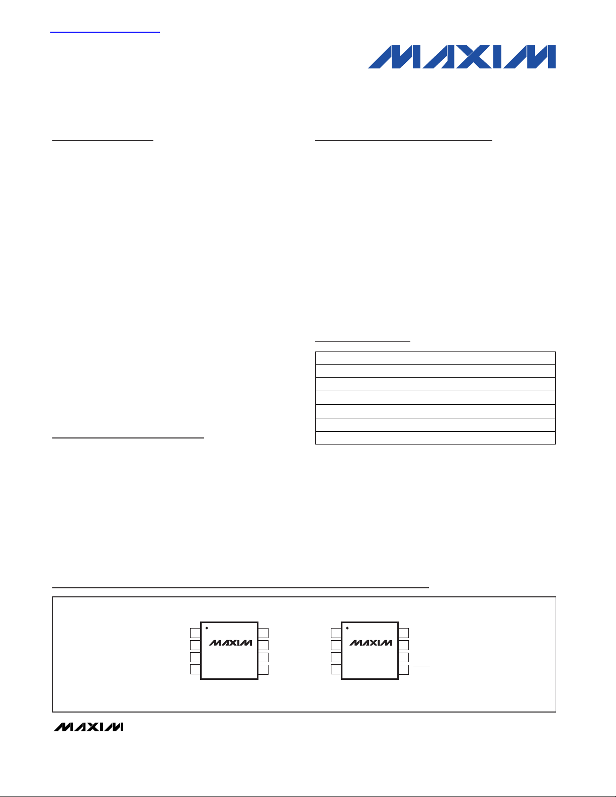
The MAX7500 features three address select lines, while
the MAX7501 and MAX7502 feature two address select
lines and a RESET input. The MAX7500/MAX7501/
MAX7502s’ 3.0V to 5.5V supply voltage range, low
250µA supply current, and a lockup-protected I2Ccompatible interface make them ideal for a wide range
of applications, including personal computers (PCs),
electronic test equipment, and office electronics.
The MAX7500/MAX7501/MAX7502 are available in 8pin µMAX®and SO packages and operate over the
-55°C to +125°C temperature range.
Applications
PCs
Servers
Office Electronics
Electronic Test Equipment
Industrial Process Control
Features
♦ Timeout Prevents Bus Lockup
♦ I2C Bus Interface
♦ 3.0V to 5.5V Supply Voltage Range
♦ 250µA (typ) Operating Supply Current
♦ 3µA (typ) Shutdown Supply Current
♦ ±2°C (max) from -25°C to +100°C Temperature
Accuracy
♦ µMAX, SO Packages Save Space
♦ Separate Open-Drain OS Output Operates as
Interrupt or Comparator/Thermostat Input
♦ Register Readback Capability
♦ Improved LM75 Second Source
MAX7500/MAX7501/MAX7502
Digital Temperature Sensors and Thermal
Watchdog with Bus Lockup Protection
________________________________________________________________ Maxim Integrated Products 1
1
2
3
4
8
7
6
5
+V
S
A0
A1
A2GND
OS
SCL
SDA
MAX7500
µMAX, SO
1
2
3
4
8
7
6
5
+V
S
A0
A1
RESETGND
OS
SCL
SDA
MAX7501
MAX7502
µMAX, SO
TOP VIEW
Pin Configurations
Ordering Information
19-3382; Rev 1; 10/04
For pricing, delivery, and ordering information, please contact Maxim/Dallas Direct! at
1-888-629-4642, or visit Maxim’s website at www.maxim-ic.com.
PART TEMP RANGE PIN-PACKAGE
MAX7500MSA -55°C to +125°C 8 SO
MAX7500MUA -55°C to +125°C 8 µMAX
MAX7501MSA -55°C to +125°C 8 SO
MAX7501MUA -55°C to +125°C 8 µMAX
MAX7502MSA -55°C to +125°C 8 SO
MAX7502MUA -55°C to +125°C 8 µMAX
Purchase of I2C components from Maxim Integrated Products
Inc., or one of its sublicensed Associated Companies, conveys
a license under Philips I
2
C Patent Rights to use these compo-
nents in an I
2
C system, provided that the system conforms to
the I
2
C Standard Specification as defined by Philips.
I
2
C is a trademark of Philips Corp.
µMAX is a registered trademark of Maxim Integrated
Products, Inc.
查询MAX7500供应商

MAX7500/MAX7501/MAX7502
Digital Temperature Sensors and Thermal
Watchdog with Bus Lockup Protection
2 _______________________________________________________________________________________
ABSOLUTE MAXIMUM RATINGS
ELECTRICAL CHARACTERISTICS
(+VS = +3.0V to +5.5V, TA= -55°C to +125°C, unless otherwise noted. Typical values are at +VS= +3.3V, TA= +25°C.) (Notes 4, 5)
Stresses beyond those listed under “Absolute Maximum Ratings” may cause permanent damage to the device. These are stress ratings only, and functional
operation of the device at these or any other conditions beyond those indicated in the operational sections of the specifications is not implied. Exposure to
absolute maximum rating conditions for extended periods may affect device reliability.
Note 1: Absolute Maximum Ratings indicate limits beyond which damage to the device may occur. DC and AC electrical specifica-
tions do not apply when operating the device beyond its rated operating conditions.
Note 2: When the input voltage (V
I
) at any pin exceeds the power supplies (VI< GND or VI> + VS), the current at that pin should be
limited to 5mA. The 20mA maximum package input current rating limits the number of pins that can safely exceed the power
supplies with an input current of 5mA to 4.
Note 3: Human Body Model, 100pF discharged through a 1.5kΩ resistor.
(Note 1)
+V
S
to GND ............................................................. -0.3V to +6V
OS, SDA, SCL to GND.......................................... -0.3V to +6.0V
All Other Pins to GND................................ -0.3V to (+V
S
+ 0.3V)
Input Current at Any Pin (Note 2) ..................................... +5mA
Package Input Current (Note 2) ..................................... +20mA
ESD Protection (all pins, Human Body Model, Note 3)... ±2000V
Continuous Power Dissipation (T
A
= +70°C)
8-Pin µMAX (derate 4.5mW/°C above +70°C) ............ 362mW
8-Pin SO (derate 5.9mW/°C above +70°C)................. 471mW
Operating Temperature Range ....................... -55°C to +125°C
Junction Temperature .................................................... +150°C
Storage Temperature Range ........................... -65°C to +150°C
Lead Temperature (soldering, 10s) ............................... +300°C
PARAMETER
CONDITIONS
UNITS
-25°C ≤ TA ≤ +100°C
Accuracy
-55°C ≤ T
A
≤ +125°C
°C
Resolution 9 Bits
Conversion Time (Note 6)
ms
I2C inactive
0.5 mA
Shutdown mode, +VS = 3V 3Quiescent Supply Current
Shutdown mode, +V
S
= 5V 5
µA
+VS Supply Voltage Range 3.0 5.5 V
OS Output Saturation Voltage I
OUT
= 4.0mA (Note 7) 0.8 V
OS Delay (Note 8) 1 6
Conver-
sions
TOS Default Temperature (Note 9) 80 °C
T
HYST
Default Temperature (Note 9) 75 °C
LOGIC (SDA, SCL, A0, A1, A2)
Input High Voltage V
IH
+VS x
0.7
V
Input Low Voltage V
IL
+VS x
0.3
V
Input High Current I
IH
VIN = 5V
1.0 µA
Input Low Current I
IL
VIN = 0V
1.0 µA
Input Capacitance All digital inputs 5 pF
Output High Current VIN = 5V 1 µA
Output Low Voltage IOL = 3mA 0.4 V
SYMBOL
MIN TYP MAX
±2.0
±3.0
100
0.25
0.005
0.005

MAX7500/MAX7501/MAX7502
Digital Temperature Sensors and Thermal
Watchdog with Bus Lockup Protection
_______________________________________________________________________________________ 3
Note 4: All parts operate properly over the +VS= 3V to 5V supply voltage range. The devices are tested and specified for rated
accuracy at their nominal supply voltage. Accuracy typically degrades 1°C per volt of change in +V
S
as it varies from the
nominal value.
Note 5: All parameters are measured at +25°C. Values over the temperature range are guaranteed by design.
Note 6: This specification indicates how often temperature data is updated. The devices can be read at any time without regard
to conversion state, while yielding the last conversion result.
Note 7: For best accuracy, minimize output loading. Higher sink currents can affect sensor accuracy due to internal heating.
Note 8: OS delay is user programmable up to six “over-limit” conversions before OS is set to minimize false tripping in noisy
environments.
Note 9: Default values set at power-up.
Note 10: All timing specifications are guaranteed by design.
Note 11: A master device must provide a hold time of at least 300ns for the SDA signal to bridge the undefined region of SCL’s
falling edge.
Note 12: C
B
= total capacitance of one bus line in pF. Tested with CB= 400pF.
Note 13: Input filters on SDA, SCL, and A_ suppress noise spikes less than 50ns.
Note 14: Holding the SDA line low for a time greater than t
TIMEOUT
causes the devices to reset SDA to the IDLE state of the serial
bus communication (SDA set high).
ELECTRICAL CHARACTERISTICS (continued)
(+VS = +3.0V to +5.5V, TA= -55°C to +125°C, unless otherwise noted. Typical values are at +VS= +5V, TA= +25°C.) (Notes 4, 5)
PARAMETER
SYMBOL
CONDITIONS
MIN
TYP
MAX
UNITS
I2C-COMPATIBLE TIMING (Note 10)
Serial Clock Frequency f
SCL
Bus timeout inactive DC 400 kHz
Minimum RESET Pulse Width 1 µs
Bus Free Time Between STOP
and START Conditions
t
BUF
1.3 µs
START Condition Hold Time t
HD:STA
0.6 µs
STOP Condition Setup Time t
SU:STO
90% of SCL to 10% of SDA 100 ns
Clock Low Period t
LOW
1.3 µs
Clock High Period t
HIGH
0.6 µs
START Condition Setup Time t
SU:STA
90% of SCL to 90% of SDA 100 ns
Data Setup Time t
SU:DAT
10% of SDA to 10% of SCL 100 ns
Data Hold Time
10% of SCL to 10% of SDA (Note 11) 0 0.9 µs
Maximum Receive SCL/SDA Rise
Time
t
R
ns
Minimum Receive SCL/SDA Rise
Time
t
R
(Note 12)
20 +
0.1 x
C
B
ns
Maximum Receive SCL/SDA Fall
Time
t
F
ns
Minimum Receive SCL/SDA Fall
Time
t
F
(Note 12)
20 +
0.1 x
C
B
ns
Transmit SDA Fall Time t
F
(Note 12)
20 +
0.1 x
C
B
250 ns
t
SP
(Note 13) 0 50 ns
SDA Time Low for Reset of Serial
Interface
(Note 14) 150 300 ms
t
HD:DAT
300
300
Pulse Width of Suppressed Spike
t
TIMEOUT

MAX7500/MAX7501/MAX7502
Digital Temperature Sensors and Thermal
Watchdog with Bus Lockup Protection
4 _______________________________________________________________________________________
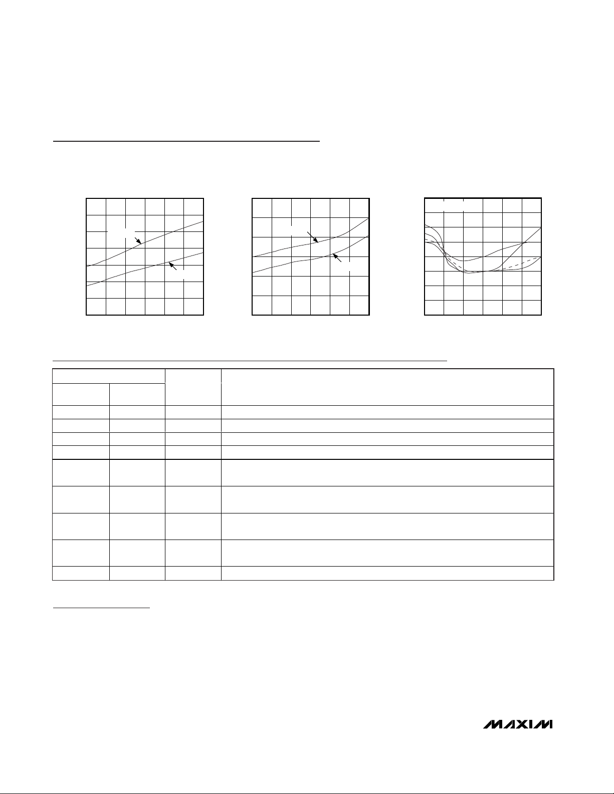
Typical Operating Characteristics
(TA = +25°C, unless otherwise noted.)
QUIESCENT SUPPLY CURRENT
vs. TEMPERATURE
MAX7500 toc01
TEMPERATURE (°C)
QUIESCENT SUPPLY CURRENT (µA)
9565355-25
240
250
260
270
280
290
300
230
-55 125
+VS = +5V
+VS = +3V
SHUTDOWN SUPPLY CURRENT (µA)
1
2
3
4
5
6
0
SHUTDOWN SUPPLY CURRENT
vs. TEMPERATURE
MAX7500 toc02
TEMPERATURE (°C)
9565355-25-55 125
+VS = +5V
+VS = +3V
ACCURACY vs. TEMPERATURE
ACCURACY (°C)
-1.5
-1.0
-0.5
0
0.5
1.0
1.5
2.0
-2.0
MAX7500 toc03
TEMPERATURE (°C)
9565355-25-55 125
4 TYPICAL PARTS
Pin Description
PIN
MAX7501
NAME FUNCTION
1 1 SDA Serial Data Input/Output Line. Open drain. Connect SDA to a pullup resistor.
2 2 SCL Serial Data Clock Input. Open drain. Connect SCL to a pullup resistor.
3 3 OS Over-Temperature Shutdown Output. Open drain. Connect OS to a pullup resistor.
4 4 GND Ground
5 — A2
2-Wire Interface Address Input. Connect A2 to GND or +V
S
to set the desired I2C bus
address. Do not leave floating. (See Table 1.)
— 5 RESET
Active-Low Reset Input. Pull RESET low for longer than the minimum reset pulse width
to reset the I
2
C bus and all internal registers to their POR values.
66A1
2-Wire Interface Address Input. Connect A1 to GND or +V
S
to set the desired I2C bus
address. Do not leave floating. (See Table 1.)
77A0
2-Wire Interface Address Input. Connect A0 to GND or +V
S
to set the desired I2C bus
address. Do not leave floating. (See Table 1.)
88+V
S
Positive Supply Voltage Input. Bypass to GND with a 0.1µF bypass capacitor.
Detailed Description
The MAX7500/MAX7501/MAX7502 temperature sensors measure temperature, convert the data into digital
form using a sigma-delta ADC, and communicate the
conversion results through an I
2
C-compatible 2-wire
serial interface. These devices accept standard I2C
commands to read the data, set the over-temperature
alarm (OS) trip thresholds, and configure other characteristics. The MAX7500 features three address select
lines (A0, A1, A2) while the MAX7501 and MAX7502
feature two address select lines (A0, A1) and a RESET
input. The MAX7500/MAX7501/MAX7502 operate from
+3.0V to +5.5V supply voltages of and consume 250µA
of supply current.
MAX7500
MAX7502
 Loading...