Maxim MAX746C-D, MAX746CPE, MAX746CSE, MAX746EPE, MAX746ESE Datasheet
...
_______________General Description
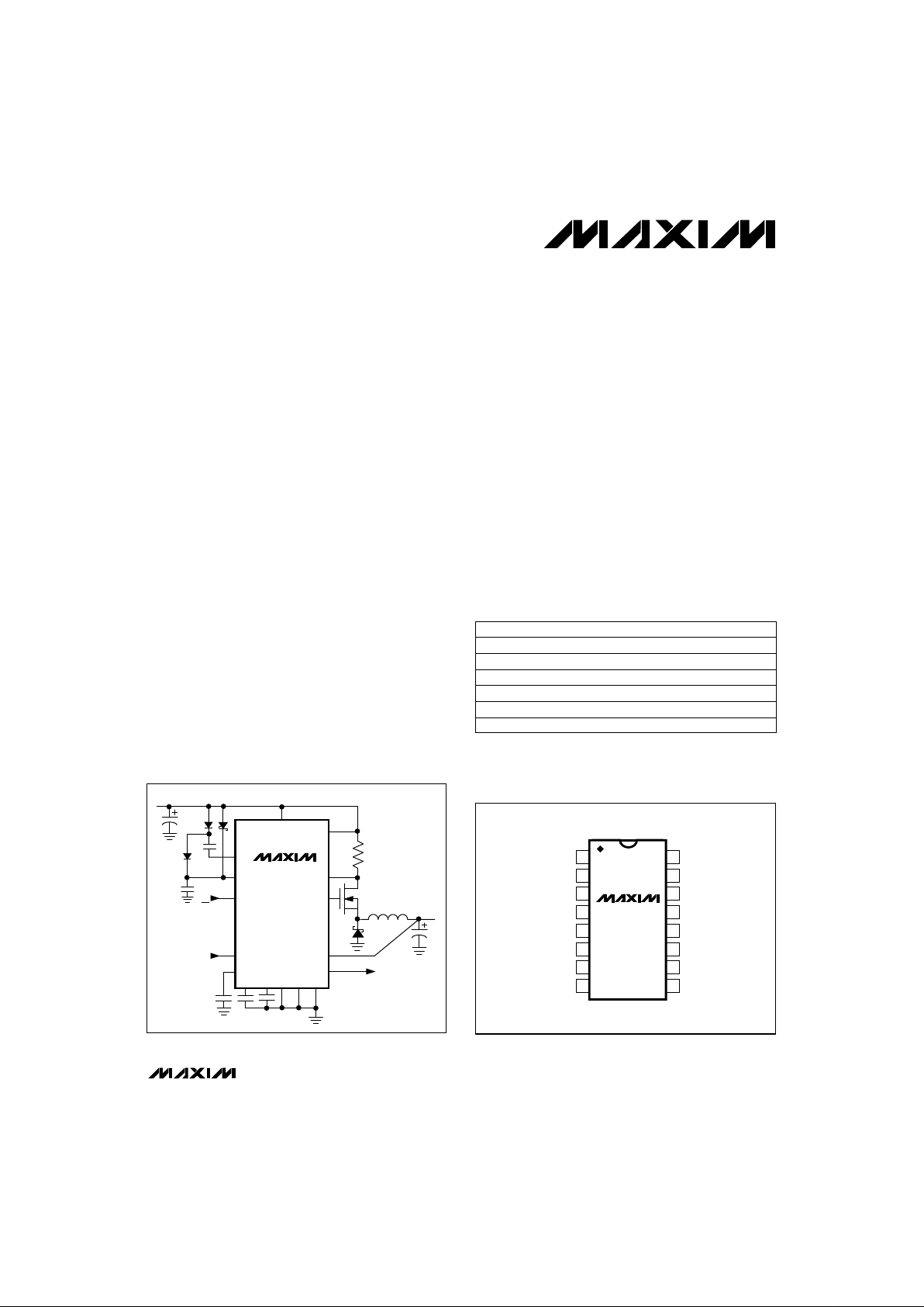
The MAX746 is a high-efficiency, high-current, step-down
DC-DC power-supply controller that drives external N-channel FETs. It provides 93% to 96% efficiency from a 6V supply
voltage with load currents ranging from 50mA up to 3A. It
uses a pulse-width-modulating (PWM) current-mode control
scheme to provide precise output regulation and low output
noise. The MAX746's 4V to 15V input voltage range, fixed
5V/adjustable (Dual-ModeTM) output, and adjustable current
limit make this device ideal for a wide range of applications.
High efficiency is maintained with light loads due to a proprietary automatic pulse-skipping control (Idle-ModeTM) scheme
that minimizes switching losses by reducing the switching frequency at light loads. The low 950µA quiescent current and
ultra-low 1.4µA shutdown current further extend battery life.
External components are protected by the MAX746's cycleby-cycle current limit. The MAX746 also features a 2V ±1.5%
reference, a comparator for low-battery detection or level
translating, and soft-start and shutdown capability.
The MAX747—discussed in aseparatedata sheet—
functions similarly to the MAX746, but drives P-channel logic
level FETs.
________________________Applications
5V-to-3.3V Green PC Applications
Notebook/Laptop Computers
Personal Digital Assistants
Battery-Operated Equipment
Cellular Phones
____________________________Features
♦ 93% to 96% Efficiency for 50mA to 3A
Output Currents
♦ 4V to 15V Input Voltage Range
♦ Low 950µA Supply Current
♦ 1.4µA Shutdown Current
♦ Drives External N-Channel FETs
♦ Fixed-Frequency Current-Mode PWM (Heavy Loads)
♦ Idle-Mode PFM (Light Loads)
♦ Cycle-by-Cycle Current Limiting
♦ 2V ±1.5% Accurate Reference Output
♦ Adjustable Soft-Start
♦ Undervoltage Lockout
♦ Precision Comparator for Power-Fail or
Low-Battery Warning
______________Ordering Information
* Contact factory for dice specifications.
MAX746
High-Efficiency, PWM, Step-Down,
N-Channel DC-DC Controller
________________________________________________________________
Maxim Integrated Products
1
16
15
14
13
12
11
10
9
1
2
3
4
5
6
7
8
GND
V+
CP
HIGH
REF
SS
LBI
LBO
TOP VIEW
MAX746
EXT
AGND
CS
OUT
AV+
CC
FB
SHDN
DIP/SO
__________________Pin Configuration
CP
HIGH
SHDN
LBI
REF
EXT
OUT
V+
AV+
CS
OUTPUT
5V
LOW-BATTERY
DETECTOR OUTPUT
LBO
GND
AGND
FB
CC
SS
ON/OFF
LOW-BATTERY
DETECTOR INPUT
INPUT 6V TO 15V
40mΩ
39µH
440µF
MAX746
__________Typical Operating Circuit
Call toll free 1-800-998-8800 for free samples or literature.
PART TEMP. RANGE PIN-PACKAGE
MAX746CPE 0°C to +70°C 16 Plastic DIP
MAX746CSE 0°C to +70°C 16 Narrow SO
MAX746C/D 0°C to +70°C Dice*
MAX746MJE -55°C to +125°C 16 CERDIP
MAX746ESE -40°C to +85°C 16 Narrow SO
MAX746EPE -40°C to +85°C 16 Plastic DIP
19-0192; Rev 1; 11/93
™Dual-Mode and Idle-Mode are trademarks of Maxim Integrated Products.
MAX746
High-Efficiency, PWM, Step-Down,
N-Channel DC-DC Controller
2 _______________________________________________________________________________________
ABSOLUTE MAXIMUM RATINGS
Supply Voltage V+, AV+ to GND..............................-0.3V to 17V
HIGH, EXT to GND....................................................-0.3V to 21V
AGND to GND..........................................................-0.3V to 0.3V
All Other Pins................................................-0.3V to (V+ + 0.3V)
Reference Current (I
REF
)....................................................±2mA
Continuous Power Dissipation (T
A
= +70°C)
Plastic DIP (derate 10.53mW/°C above +70°C) ..........842mW
Narrow SO (derate 8.70mW/°C above +70°C) ............696mW
CERDIP (derate 10.00mW/°C above +70°C)...............800mW
Operating Temperature Ranges:
MAX746C_E........................................................0°C to +70°C
MAX746E_E.....................................................-40°C to +85°C
MAX746MJE ..................................................-55°C to +125°C
Junction Temperatures:
MAX746C_E/E_E..........................................................+150°C
MAX746MJE.................................................................+175°C
Storage Temperature Range.............................-65°C to +160°C
Lead Temperature (soldering, 10sec).............................+300°C
ELECTRICAL CHARACTERISTICS
(V+ = 10V, I
LOAD
= 0A, I
REF
= 0µA, TA= T
MIN
to T
MAX
, unless otherwise noted.)
Stresses beyond those listed under “Absolute Maximum Ratings” may cause permanent damage to the device. These are stress ratings only, and functional
operation of the device at these or any other conditions beyond those indicated in the operational sections of the specifications is not implied. Exposure to
absolute maximum rating conditions for extended periods may affect device reliability.
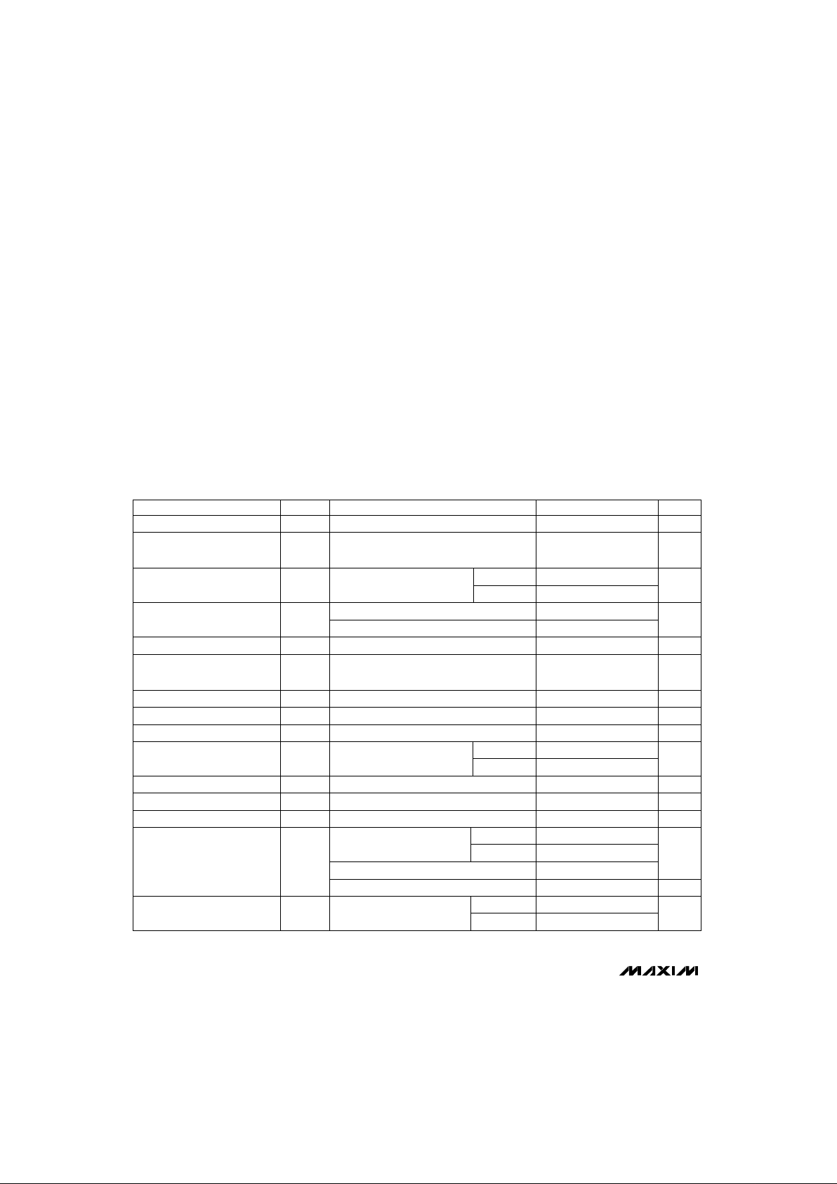
PARAMETER SYMBOL MIN TYP MAX UNITS
Efficiency 94 %
Load Regulation 1.3 2.5 %
Line Regulation
0.1
%/V
OUT Leakage Current 50 80
µA
FB Input Logic Low 40 mV
Output Voltage
Input Voltage 415V
V
OUT
4.85 5.08 5.25 V
Feedback Voltage V
FB
V
Reference Voltage V
REF
1.96 2.00 2.04
Reference Load Regulation 920mV
Soft-Start Source Current 0.5 1.0 1.5
µA
Soft-Start Fault Current (Note 1) 100 500
µA
Supply Current (Note 2) I
SUPP
1.7
mA
0.95
1.4 20
µA
Oscillator Frequency f
OSC
80 100 120
kHz
CONDITIONS
I
REF
= 0µA to 100µA
0V < (V+ - CS) < 0.125V
V+ = 4V to 15V, external feedback mode
V
OUT
= 5V
For dual-mode switchover
SS = 0V
SS = 2V
Operating, V+ = 15V
Operating, V+ = 10V
Shutdown mode
(V+ - CS) = 0V,
external feedback mode
FB Input Leakage Current 1 100 nAFB = 2V
I
REF
= 0µA
MAX746E/M
MAX746E/M 1.95 2.00 2.05
MAX746C
V+
V+ = 6V to 15V, 0V < (V+ - CS) < 0.125V,
FB = 0V (includes line and load regulation)
MAX746C 1.96 2.00 2.04
V+ = 6V to 15V, FB = 0V 0.05
Circuit of Figure 1, I
LOAD
= 0.5A to 2.5A,
V+ = 6V
1.97 2.00 2.03
V
MAX746E/M
MAX746C 1.1 1.4
MAX746E/M
85 100 115MAX746C
MAX746
High-Efficiency, PWM, Step-Down,
N-Channel DC-DC Controller
_______________________________________________________________________________________ 3
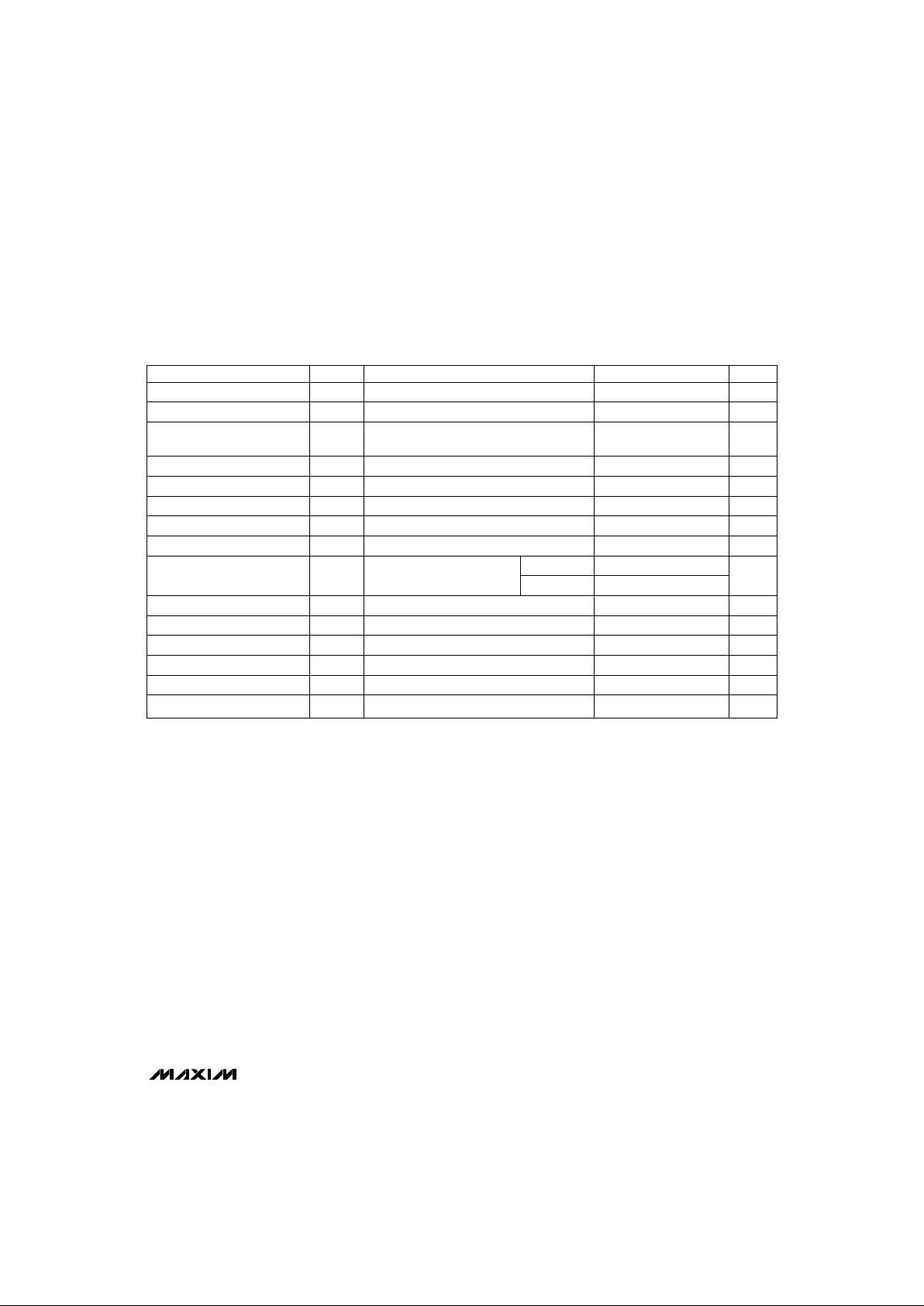
Note 1: The soft-start fault current is the current sink capability of SS when V
REF
< 1V or when the device is in shutdown.
Note 2: I
SUPP
is the supply current drawn by V+, which includes the current drawn by the charge pump. The charge pump
doubles the current drawn by HIGH from the V+ input, so I
SUPP
= IV++ 2I
HIGH
.
ELECTRICAL CHARACTERISTICS (continued)
(V+ = 10V, I
LOAD
= 0A, I
REF
= 0µA, TA= T
MIN
to T
MAX
, unless otherwise noted.)
PARAMETER
SHDN Input Leakage Current
SYMBOL MIN TYP MAX UNITS
LBO Output Voltage Low V
OL
nA
0.4 V
LBI Threshold Voltage
1.96 2.00 2.04
V
Compensation Pin Impedance 24
kΩ
EXT Source Current 270 mA
LBI Input Leakage Current nA
LBO Output Leakage Current 1
µA
SHDN Input Voltage Low V
IL
0.4 V
SHDN Input Voltage High V
IH
2.0 V
EXT Output Low
EXT Output High V
HIGH
- 0.1 V
0.25 V
EXT Sink Current 160 mA
MAX746E/M
CONDITIONS
SHDN = 10V
I
SINK
= 0.5mA
LBI falling
V
HIGH
= 15V, V
EXT
= 2.5V
LBI = 2.5V
V+ = 15V, LBO = 15V, LBI = 2.5V
V
HIGH
forced to 15V, I
EXT
= -1mA
V
HIGH
forced to 15V, I
EXT
= 1mA
V
HIGH
= 15V, V
EXT
= 12.5V
MAX746C 1.97 2.00 2.03
100
0.1 100
Charge-Pump Output Voltage
Maximum Duty Cycle 91 96 %
V
HIGH
V+ + 4 V+ + 5 V+ + 6 V
V
LIMIT
125 150 175 mV
V+ = 6V
I
HIGH
= 0mA to 10mA
V+ – CS
Current-Sense Amplifier
Current-Limit Threshold
MAX746
High-Efficiency, PWM, Step-Down,
N-Channel DC-DC Controller
4 _______________________________________________________________________________________
N0-LOAD SUPPLY CURRENT
vs. SUPPLY VOLTAGE
NO-LOAD SUPPLY CURRENT (mA)
0.8
0.9
1.0
1.1
1.2
579111315
SUPPLY VOLTAGE (V)
MAX746-01
0
-75
NO-LOAD SUPPLY CURRENT
vs. TEMPERATURE
MAX746-02
TEMPERATURE (°C)
NO-LOAD SUPPLY CURRENT (mA)
3
1
4
2
-50 -25 0 25 50 75 100 125
V+ = 9V
V
OUT
= 5V
ENTIRE
CIRCUIT
SCHOTTKY DIODE
LEAKAGE EXCLUDED
4
0
0.01
PEAK INDUCTOR CURRENT
vs. OUTPUT CURRENT
1
2
MAX746-03
OUTPUT CURRENT (A)
PEAK INDUCTOR CURRENT (A)
3
0.1 1 10
VIN = 12V
VIN = 9V
VIN = 6V
CIRCUIT OF FIGURE 1a
V
OUT
= 5V
1.5
0
0.01
PEAK INDUCTOR CURRENT
vs. OUTPUT CURRENT
0.5
MAX746-03
OUTPUT CURRENT (A)
PEAK INDUCTOR CURRENT (A)
1.0
0.1 1
CIRCUIT OF FIGURE 1c
V
OUT
= 5V
VIN = 12V
VIN = 6V
10
100
70
0.01
EFFICIENCY vs. OUTPUT CURRENT
80
MAX746-07
OUTPUT CURRENT (A)
EFFICIENCY (%)
90
0.1 1 10
VIN = 12V
VIN = 9V
VIN = 6V
CIRCUIT OF FIGURE 1a
V
OUT
= 5V
4
0
0.01
PEAK INDUCTOR CURRENT
vs. OUTPUT CURRENT
1
2
MAX746-05
OUTPUT CURRENT (A)
PEAK INDUCTOR CURRENT (A)
3
0.1 1 10
CIRCUIT OF FIGURE 1b
V
OUT
= 3.3V
V+ = 5V
100
70
0.01
EFFICIENCY vs. OUTPUT CURRENT
80
MAX746-06
OUTPUT CURRENT (A)
EFFICIENCY (%)
90
0.1 1 10
CIRCUIT OF FIGURE 1c
VIN = 12V
VIN = 6V
V
OUT
= 5V
100
70
0.01
EFFICIENCY vs. OUTPUT CURRENT
80
MAX746-08
OUTPUT CURRENT (A)
EFFICIENCY (%)
90
0.1 1 10
CIRCUIT OF FIGURE 1b
V
OUT
= 3.3V
V+ = 5V
CONTINUOUS-CONDUCTION MODE
BOUNDARY AND CORRESPONDING
PEAK INDUCTOR CURRENT
SUPPLY VOLTAGE (V)
5
7
9
11
13
0.7
OUTPUT CURRENT (A)
15
MAX746-09
0.9 1.1 1.3 1.5 1.7
DISCONTINUOUS-
CONDUCTION REGION
CONTINUOUS-
CONDUCTION
REGION
PEAK
INDUCTOR
CURRENT
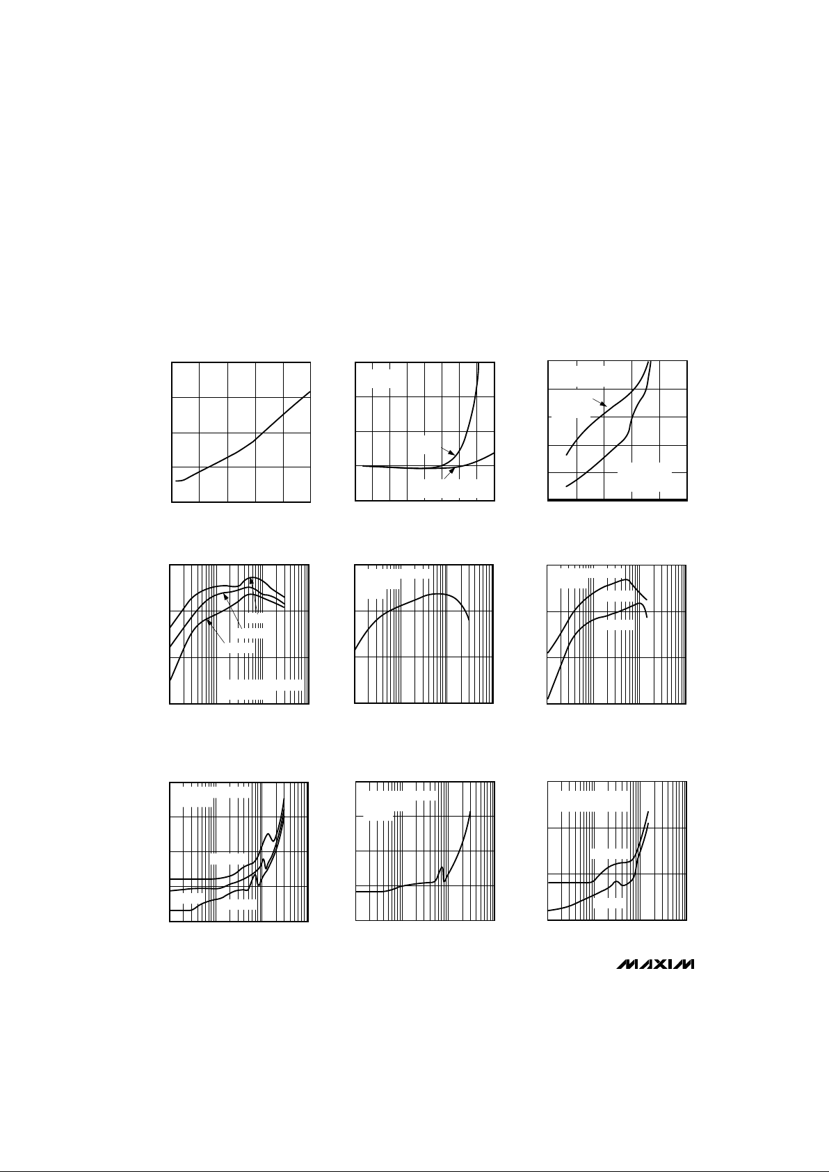
__________________________________________Typical Operating Characteristics
(Circuit of Figure 1a, TA = +25°C, unless otherwise noted.)
MAX746
High-Efficiency, PWM, Step-Down,
N-Channel DC-DC Controller
_______________________________________________________________________________________
5
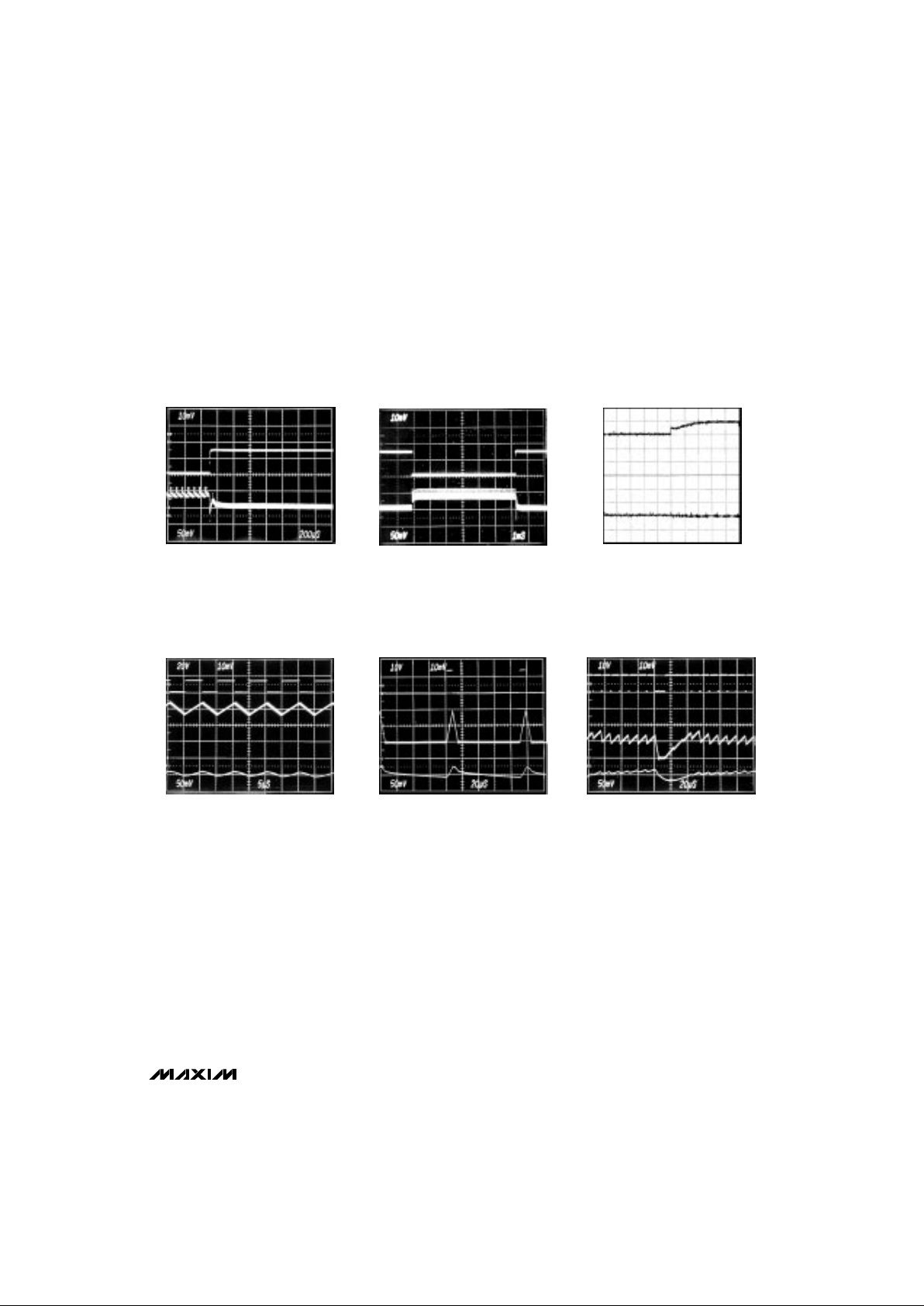
A: LOAD CURRENT, 0.1A TO 1.5A, 1A/div
B: V
OUT
RIPPLE, 50mV/div, AC-COUPLED
V+ = 10V
LOAD-TRANSIENT RESPONSE
A
B
200µs/div
A: EXT VOLTAGE, 10V/div
B: INDUCTOR CURRENT, 500mA/div
C: V
OUT
RIPPLE, 50mV/div, AC-COUPLED
V+ = 6V, I
OUT
= 480mA
A
B
MODERATE-LOAD, IDLE-MODE
WAVEFORMS
20µs/div
C
A: LOAD CURRENT, 0.1A TO 1.5A, 1A/div
B: V
OUT
RIPPLE, 50mV/div, AC COUPLED
V+ = 10V
LOAD-TRANSIENT RESPONSE
A
B
1ms/div
A : EXT VOLTAGE, 20V/div
B : INDUCTOR CURRENT 1A/div
C : V
OUT
RIPPLE, 50mV/div
V+ = 10V, I
OUT
= 3A
CONTINUOUS-CONDUCTION MODE
WAVEFORMS
A
B
C
5µs/div
0V
8V
A: V+ = 8V TO 10V, 2V/div
B: V
OUT
RIPPLE, 100mV/div
I
OUT
= 3A
LINE-TRANSIENT RESPONSE
A
B
10V
500ms/div
A: EXT VOLTAGE, 10V/div
B: INDUCTOR CURRENT, 500mA/div
C: V
OUT
RIPPLE, 50mV/div, AC-COUPLED
V+ = 10V, I
OUT
= 75mA
DISCONTINUOUS-CONDUCTION
IDLE-MODE WAVEFORMS
A
B
20µs/div
C
____________________________Typical Operating Characteristics (continued)
(Circuit of Figure 1a, TA = +25°C, unless otherwise noted.)
 Loading...