Maxim MAX7469, MAX7470UTP+ Datasheet

General Description
The MAX7469/MAX7470 triple-channel, anti-aliasing filters and buffers are ideal for high-definition (HD) and
standard-definition (SD) television (TV) applications.
Compatible with 1080i, 720p, 720i, 480p, and 480i
scanning system standards and computer format signals, the MAX7469/MAX7470 support component video
(Y P
bPr
, GsBR, and RGBHV), as well as composite
(CVBS) and S-video (Y/C).
The MAX7469/MAX7470 limit the input bandwidth for
anti-aliasing and out-of-band noise reduction prior to
digital conversion by an ADC or video decoder. The
MAX7469/MAX7470 frequency response can be continuously varied in 256 linear steps through an I2C* interface from below SD resolution to beyond HD resolution.
The output buffers of the MAX7469/MAX7470 drive a
2V
P-P
video signal into a standard 150Ω load. The inputs
are AC-coupled, and the outputs can be either DC- or
AC-coupled. The MAX7469 has a gain of 0dB, and the
MAX7470 has a gain of +6dB. Both devices are available
in a 20-pin TQFN package and are fully specified over
the 0°C to +85°C upper-commercial temperature range.
Applications
HDTV (LCD, PDP, DLP, CRT)
Set-Top Boxes
Personal Video Recorders
Home Theaters
Features
Continuously Variable Anti-Aliasing Filter
5MHz to 34MHz in 256 Steps
Supports All Standard Video and Computer Input
Formats
480i, 480p, 720i, 720p, 1080i
QVGA, VGA, SVGA, XGA, SXGA, UXGA
Y P
b Pr
, GsBR, RGBHV, Y/C, CVBS
Accepts Any Input Sync Format
Sync on Y, Sync on G, External Sync (Positive
or Negative)
Sync on All Channels
Buffered Outputs Drive Standard 150Ω Video
Load
0dB (MAX7469)
+6dB (MAX7470)
DC- or AC-Coupled Outputs
Single +5V Analog and +3.3V Digital Supplies
5mW Power-Down Mode
20-Pin TQFN Lead-Free Package
MAX7469/MAX7470
PART
PIN-PACKAGE
BUFFER
GAIN (dB)
PKG
CODE
M A X7 4 6 9 U TP + 20 TQFN-EP* 0
T2055-4
M A X7 4 7 0 U TP + **
20 TQFN-EP* +6
T2055-4
Ordering Information
19-0548; Rev 0; 5/06
HDTV Continuously Variable
Anti-Aliasing Filters
Typical Operating Circuit appears at end of data sheet.
*
Purchase of I2C components from Maxim Integrated Products,
Inc., or one of its sublicensed Associate Companies, conveys a
license under the Philips I
2
C Patent Rights to use these compo-
nents in an I
2
C system, provided that the system conforms to the
I
2
C Standard Specification defined by Philips.
________________________________________________________________
Maxim Integrated Products
1
For pricing delivery, and ordering information please contact Maxim/Dallas Direct! at
1-888-629-4642, or visit Maxim’s website at www.maxim-ic.com.
Note:
All devices are specified over the 0°C to +85°C operating
temperature range.
+
Indicates lead-free packaging.
*
EP = Exposed pad.
**
Future product—contact factory for availability.
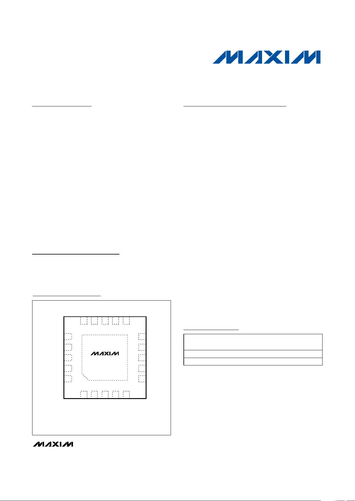
Pin Configuration
MAX7469
MAX7470
TQFN (5mm x 5mm)
*EXPOSED PAD.
SEE PIN DESCRIPTION FOR CONNECTION.
TOP VIEW
19
20
18
17
7
6
8
EXTSYNC
SDA
DV
DD
9
DGND
GND
A0
AV
DD
GND
12
IN2
45
15 14 12 11
GND
IN3
AV
DD
OUT2
AV
DD
OUT3
SCL
A1
3
13
GND
16
10
OUT1
IN1
+
*EP

MAX7469/MAX7470
HDTV Continuously Variable
Anti-Aliasing Filters
2 ________________________________________________________________________________________
AVDDto GND............................................................-0.3V to +6V
DV
DD
to DGND.........................................................-0.3V to +4V
IN_, EXTSYNC to GND .................................................................
..................................-0.3V to the lower of (AV
DD
+ 3V) and +6V
OUT_ to GND ...............................................................................
..................................-0.3V to the lower of (AV
DD
+ 3V) and +6V
A_ to GND ....................................................................................
..................................-0.3V to the lower of (AV
DD
+ 3V) and +6V
SCL, SDA to DGND ..................................................-0.3V to +6V
Continuous Power Dissipation (TA= +70°C)
20-Pin TQFN (derate 33.3mW/°C above +70°C) ...2666.7mW
Maximum Current into IN_, A_, GND,
SCL, SDA, and EXTSYNC............................................±50mA
Operating Temperature Range...............................0°C to +85°C
Storage Temperature Range .............................-65°C to +150°C
Junction Temperature......................................................+150°C
Lead Temperature (soldering, 10s) .................................+300°C
ABSOLUTE MAXIMUM RATINGS
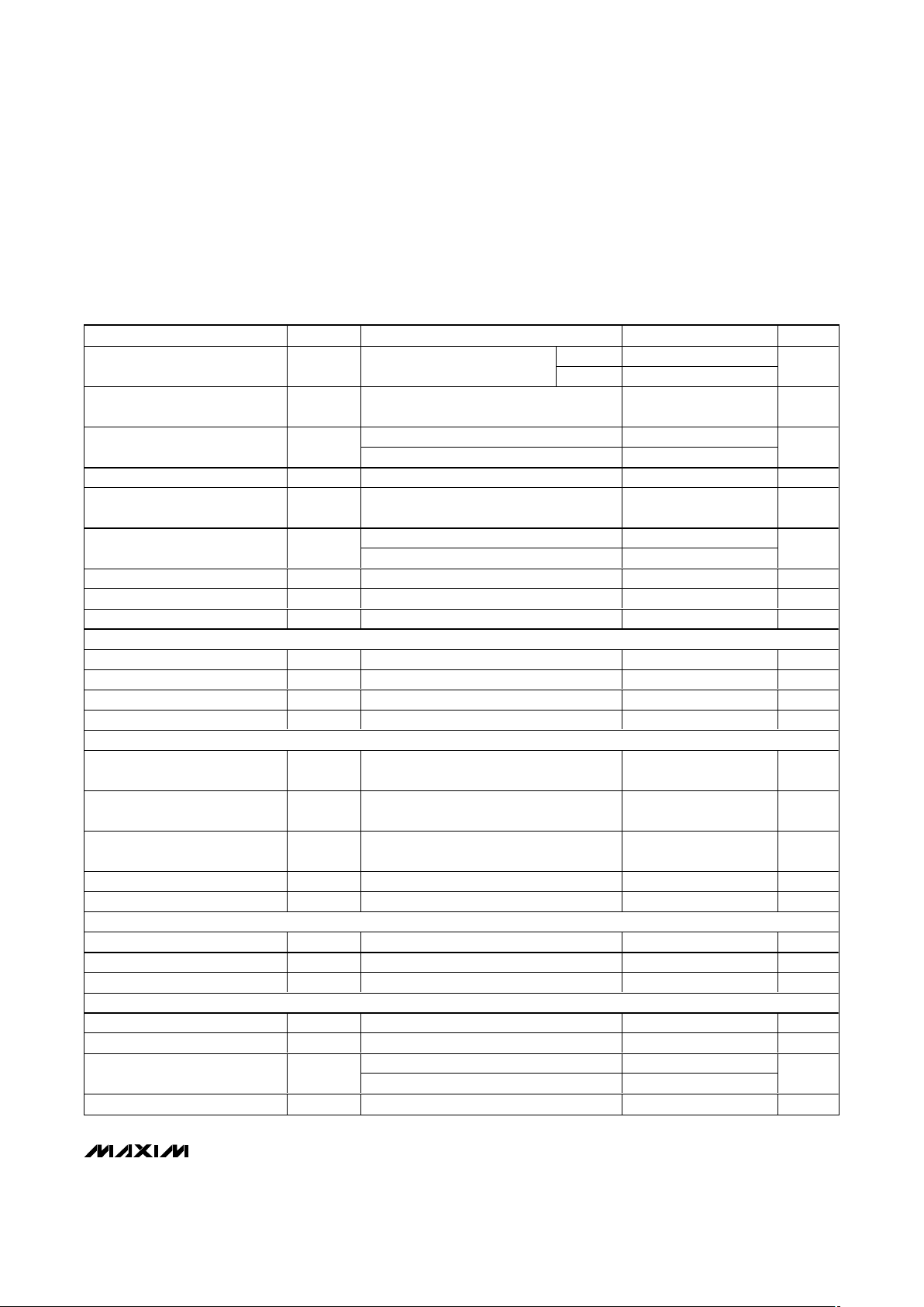
ELECTRICAL CHARACTERISTICS
(AVDD= +5V ±5%, DVDD= 2.7V to 3.6V, R
LOAD
= 150Ω to GND, CIN= 0.1µF, TA= 0°C to +85°C, unless otherwise noted. Typical
values are at AV
DD
= 5V, DVDD= 3.3V, TA= +25°C.)
PARAMETER SYMBOL CONDITIONS MIN TYP MAX UNITS
HD: f = 100kHz to 30MHz, relative to
100kHz (Note 1)
-3 -0.6 +1
Filter Passband Response A
PB
SD: f = 100kHz to 5.75MHz, relative to
100kHz (Note 2)
±0.1 ±1.0
dB
HD: f = 74MHz (Note 1) 45 57
Filter Stopband Attenuation A
SB
SD: f = 27MHz (Note 2) 52 63
dB
HD: 100kHz to 30MHz, relative to 100kHz
(Note 1)
20
Group Delay Deviation Δt
G
SD: 100kHz to 5.75MHz, relative to 100kHz
(Note 2)
15
ns
HD: channel to channel, 100kHz to 2MHz,
(Note 1)
5
Group Delay Matching t
G(MATCH
)
SD: channel to channel, 100kHz to 500kHz,
(Note 2)
1.5
ns
Bypass Frequency Response
-3dB, bypass mode, independent of filter
setting
100 MHz
SD Differential Gain dG Five-step modulated staircase (Note 2) 0.25 %
SD Differential Phase dφ Five-step modulated staircase (Note 2) 0.25 Degrees
Signal-to-Noise Ratio SNR
Output signal (2V
P-P
) to RMS noise (100kHz
to 30MHz), f = 30MHz
69 dB
SD Line-Time Distortion H
DIST
Deviations in a line with an 18µs, 100 IRE
bar; 1 line = 63.5µs (Note 2)
0.3 %
SD Field-Time Distortion V
DIST
Deviations in 130 lines with 18µs, 100 IRE
bars (Note 2)
0.3 %
Stresses beyond those listed under “Absolute Maximum Ratings” may cause permanent damage to the device. These are stress ratings only, and functional
operation of the device at these or any other conditions beyond those indicated in the operational sections of the specifications is not implied. Exposure to
absolute maximum rating conditions for extended periods may affect device reliability.

MAX7469/MAX7470
HDTV Continuously Variable
Anti-Aliasing Filters
_______________________________________________________________________________________
3
ELECTRICAL CHARACTERISTICS (continued)
(AVDD= +5V ±5%, DVDD= 2.7V to 3.6V, R
LOAD
= 150Ω to GND, CIN= 0.1µF, TA= 0°C to +85°C, unless otherwise noted. Typical
values are at AV
DD
= 5V, DVDD= 3.3V, TA= +25°C.)
PARAMETER SYMBOL CONDITIONS MIN TYP MAX UNITS
Positive 350
Clamp Settling Time
To 1% with 100 IRE step
(Note 4)
Negative 650
H
Minimum Functional Input Sync
Amplitude
125 mV
MAX7469 -0.5 0 +0.5
Low-Frequency Gain (Note 1)
MAX7470 5.5 6 6.5
dB
Low-Frequency Gain Matching 100kHz 0.05 dB
Maximum Output Voltage
Amplitude
DC to 30MHz 2.4 V
P-P
MAX7469 2.4
Maximum Input Voltage
Amplitude
MAX7470 1.2
V
P-P
Channel-to-Channel Isolation 62 dB
Output Clamping Level Variation (Notes 1, 4) ±100 mV
Power-Supply Rejection Ratio PSRR DC 50 dB
DIGITAL INPUTS (EXTSYNC, A1, A0)
Input Logic-High Voltage V
IH
2.0 V
Input Logic-Low Voltage V
IL
0.8 V
Input Leakage Current I
IN
VIN = 0 to DV
DD
±1 ±10 µA
Input Capacitance C
IN
6pF
DIGITAL INPUTS (SDA, SCL)
Input Logic-High Voltage V
IH
0.7 x
DV
DD
V
Input Logic-Low Voltage V
IL
0.3 x
DV
DD
V
Input Hysteresis V
HYST
0.05 x
DV
DD
V
Input Leakage Current I
IN
VIN = 0 to DV
DD
±0.1 ±10 µA
Input Capacitance C
IN
6pF
DIGITAL OUTPUT (SDA)
Output Logic-Low Voltage V
OL
I
SINK
= 3mA 0.4 V
Tri-State Leakage Current I
L
VIN = 0 to DV
DD
±0.1 ±10 µA
Tri-State Output Capacitance C
OUT
6pF
POWER REQUIREMENTS
Analog Supply Voltage Range AV
DD
4.75 5 5.25 V
Digital Supply Voltage Range DV
DD
2.7 3.3 3.6 V
Normal operation, no load 180 200
Analog Supply Current I
AVDD
Power-down mode, no load 1 1.5
mA
Digital Supply Current I
DVDDfSCL
= 400kHz 25 µA

MAX7469/MAX7470
HDTV Continuously Variable
Anti-Aliasing Filters
4 ________________________________________________________________________________________
TIMING CHARACTERISTICS
PARAMETER SYMBOL CONDITIONS MIN TYP MAX UNITS
Serial-Clock Frequency f
SCL
0 400 kHz
Bus Free Time Between STOP (P)
and START (S) Condition
t
BUF
1.3 µs
Hold Time (Repeated) START (Sr)
Condition
t
HD;STA
After this period, the first clock pulse is
generated
0.6 µs
SCL Pulse-Width Low t
LOW
1.3 µs
SCL Pulse-Width High t
HIGH
0.6 µs
Setup Time for a Repeated
START (Sr) Condition
t
SU;STA
0.6 µs
Data Hold Time t
HD;DAT
(Note 5) 0.0 0.9 µs
Data Setup Time t
SU;DAT
100 ns
Rise Time of Both SDA and SCL
Signals, Receiving
t
r
0 300 ns
Fall Time of Both SDA and SCL
Signals, Receiving
t
f
0 300 ns
Fall Time of SDA Signal,
Transmitting
t
f
(Note 6)
20 +
0.1C
b
250 ns
Setup Time for STOP (P)
Condition
t
SU;STO
0.6 µs
Capacitive Load for Each Bus
Line
C
b
400 pF
Pulse Width of Spikes that Are
Suppressed by the Input Filter
t
SP
(Note 7) 0 50 ns
(AVDD= +5V ±5%, DVDD= 2.7V to 3.6V, R
LOAD
= 150Ω to GND, CIN= 0.1µF, TA= 0°C to +85°C, unless otherwise noted. Typical
values are at AV
DD
= 5V, DVDD= 3.3V, TA= +25°C.)
Note 1: The filter passband edge is set to code 255.
Note 2: The filter passband edge is set to code 40.
Note 3: 1H is the total line period, depending on the video standard. For NTSC, this is 63.5µs; for HDTV, the line period is 29.64µs.
Note 4: The clamp level is at the sync tip for signals with sync pulses, and at the blanking level otherwise.
Note 5: A master device must provide a hold time of at least 300ns for the SDA signal (referred to V
IL
of the SCL signal) to bridge
the undefined region of SCL’s falling edge.
Note 6: C
b
= total capacitance of one bus line in pF. tRand tFmeasured between 0.3VDDand 0.7VDD.
Note 7: Input filters on the SDA and SCL inputs suppress noise spikes less than 50ns.

MAX7469/MAX7470
HDTV Continuously Variable
Anti-Aliasing Filters
_______________________________________________________________________________________
5
SDA
SCL
t
f
t
r
t
f
Sr
t
HD;STA
t
HD;DAT
t
HIGH
t
SU;DAT
t
SU;STA
t
HD;STA
t
SU;STO
t
SP
t
r
S SP
t
LOW
t
SP
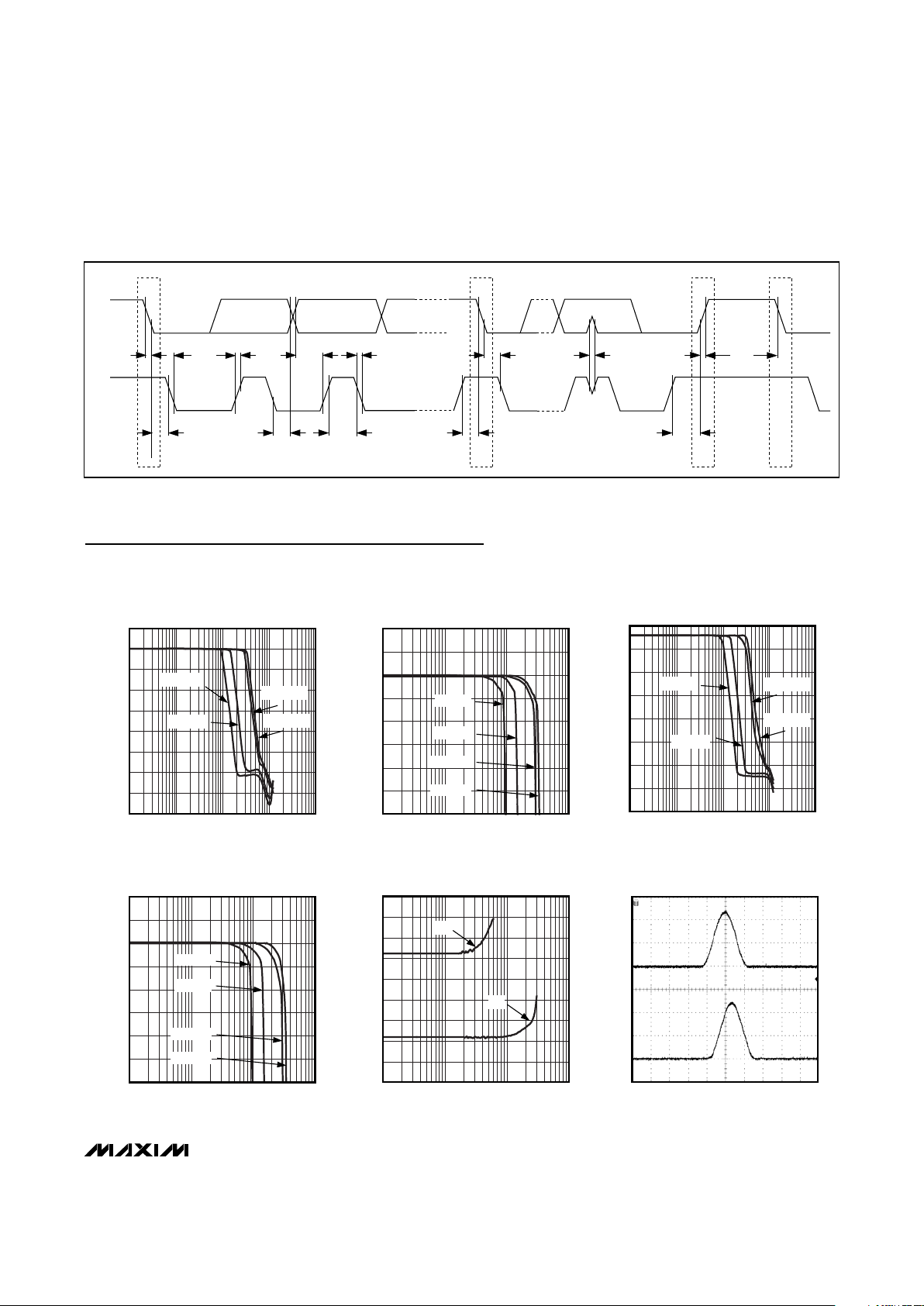
Figure 1. 2-Wire, Serial-Interface Timing Diagram
(AVDD= +5V, DV
DD
= 3.3V, R
LOAD
= 150Ω to GND, C
LOAD
= 0 to 20pF to GND, CIN= 0.1µF, TA= +25°C, unless otherwise noted.)
Typical Operating Characteristics
-80
-60
-70
-30
-40
-50
0
-10
-20
10
0.1 101 100 1000
FREQUENCY RESPONSE (MAX7469)
MAX7469 toc01
FREQUENCY (MHz)
RESPONSE (dB)
CODE 40
CODE 90
CODE 220
CODE 255
-1.5
-2.0
-2.5
-3.0
-1.0
0
-0.5
0.5
1.0
0.1 101100
PASSBAND FLATNESS (MAX7469)
MAX7469 toc02
FREQUENCY (MHz)
RESPONSE (dB)
CODE 40
CODE 255
CODE 220
CODE 90
-40
-50
-60
-70
-30
-10
-20
0
10
0.1 101 100 1000
FREQUENCY RESPONSE (MAX7470)
MAX7469 toc03
FREQUENCY (MHz)
RESPONSE (dB)
CODE 40
CODE 90
CODE 220
CODE 255
4.5
4.0
3.5
3.0
5.0
6.0
5.5
6.5
7.0
0.1 101 100
PASSBAND FLATNESS (MAX7470)
MAX7469 toc04
FREQUENCY (MHz)
RESPONSE (dB)
CODE 40
CODE 255
CODE 220
CODE 90
40
30
20
10
0
50
70
60
80
90
0.1 1 10 100
GROUP DELAY
MAX7469 toc05
FREQUENCY (MHz)
DELAY (ns)
SD
HD
200ns/div
2T RESPONSE (1 IRE = 7.14mV)
300mV/div
MAX7469 toc06
300mV/div

MAX7469/MAX7470
HDTV Continuously Variable
Anti-Aliasing Filters
6 ________________________________________________________________________________________
(AVDD= +5V, DV
DD
= 3.3V, R
LOAD
= 150Ω to GND, C
LOAD
= 0 to 20pF to GND, CIN= 0.1µF, TA= +25°C, unless otherwise noted.)
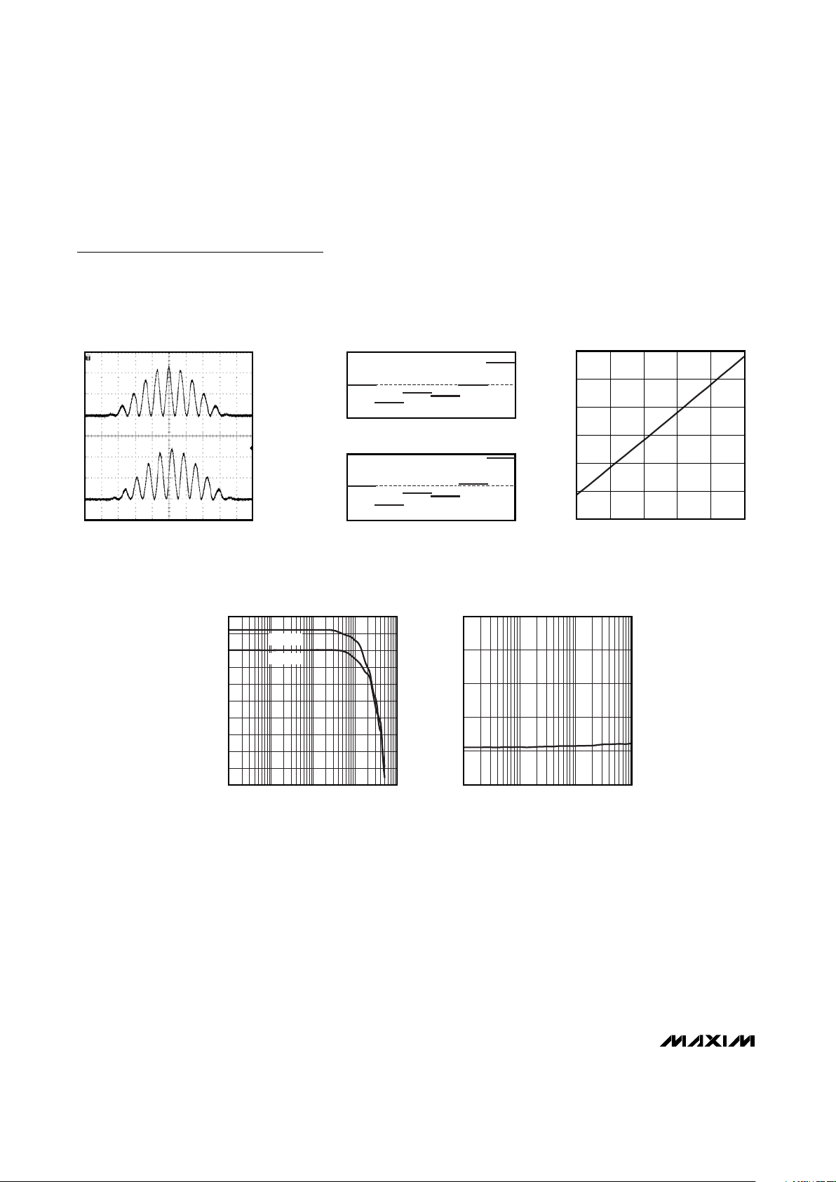
Typical Operating Characteristics (continued)
400ns/div
MODULATED 12.5T RESPONSE
(1 IRE = 7.14mV)
300mV/div
MAX7469 toc07
300mV/div
DIFFERENTIAL GAIN
MAX7469 toc08
DIFFERENTIAL PHASE (deg)
1324567
1324567
0.1
0.2
0
-0.1
-0.2
0.1
0.2
0
-0.1
-0.2
DIFFERENTIAL GAIN (%)
DIFFERENTIAL PHASE
-3dB FREQUENCY
vs. CONTROL CODE
MAX7469 toc09
CODE
MEASURED -3dB FREQUENCY (MHz)
20415310251
6
12
18
24
30
36
0
0255
-40
-10
-15
-20
-25
-30
-35
0
-5
5
10
0.1 101 100 1000
BYPASS-MODE FREQUENCY RESPONSE
MAX7469 toc10
FREQUENCY (MHz)
RESPONSE (dB)
MAX7470
MAX7469
0
4
12
8
16
20
0.1 101 100
BYPASS-MODE GROUP DELAY
MAX7469 toc11
FREQUENCY (MHz)
DELAY (ns)
 Loading...