

MAX745
Switch-Mode Lithium-Ion
Battery-Charger
________________________________________________________________
Maxim Integrated Products
1
For free samples & the latest literature: http://www.maxim-ic.com, or phone 1-800-998-8800.
For small orders, phone 1-800-835-8769.
General Description
The MAX745 provides all functions necessary for
charging lithium-ion battery packs. It provides a regulated charging current of up to 4A without getting hot,
and a regulated voltage with only ±0.75% total error at
the battery terminals. It uses low-cost, 1% resistors to
set the output voltage, and a low-cost N-channel MOSFET as the power switch.
The MAX745 regulates the voltage set point and charging current using two loops that work together to transition smoothly between voltage and current regulation.
The per-cell battery voltage regulation limit is set
between 4.0V and 4.4V using standard 1% resistors,
and then the number of cells is set from 1 to 4 by pinstrapping. Total output voltage error is less than ±0.75%.
For a similar device with an SMBus™ microcontroller
interface and the ability to charge NiCd and NiMH cells,
refer to the MAX1647 and MAX1648. For a low-cost
lithium-ion charger using a linear-regulator control
scheme, refer to the MAX846A.
____________________________Features
♦ Charges 1 to 4 Lithium-Ion Battery Cells
♦ ±0.75% Voltage-Regulation Accuracy
Using 1% Resistors
♦ Provides up to 4A without Excessive Heating
♦ 90% Efficient
♦ Uses Low-Cost Set Resistors and
N-Channel Switch
♦ Up to 24V Input
♦ Up to 18V Maximum Battery Voltage
♦ 300kHz PWM Operation: Low-Noise,
Small Components
♦ Stand-Alone Operation; No Microcontroller
Needed
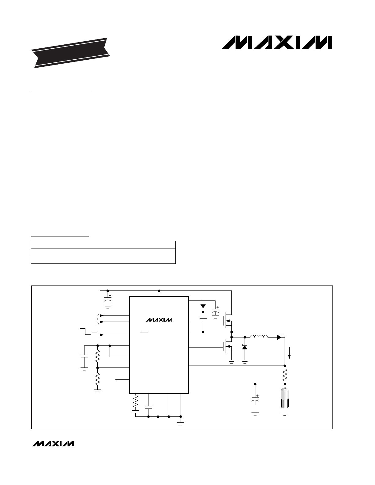
___________________________________________________Typical Operating Circuit
19-1182; Rev 2; 12/98
PART
MAX745EAP -40°C to +85°C
TEMP. RANGE PIN-PACKAGE
20 SSOP
EVALUATION KIT MANUAL
FOLLOWS DATA SHEET
Ordering Information
Pin Configuration appears on last page.
________________________Applications
Lithium-Ion Battery Packs
Desktop Cradle Chargers
Cellular Phones
Notebook Computers
Hand-Held Instruments
MAX745C/D 0°C to +70°C Dice*
*
Dice are tested at TA= +25°C.
SMBus is a trademark of Intel Corp.
(UP TO 24V)
REF
DCIN
V
IN
BST
VL
DHI
DLO
LX
CS
BATT
CELL
COUNT
SELECT
SET PER
CELL VOLTAGE
WITH 1% RESISTORS
ON
OFF
VADJ
STATUS
SETI
CELL0
CELL1
CCI PGNDGND
IBAT
CCV
N
N
I
CHARGE
R
SENSE
VOUT
1–4 Li+ CELLS
(UP TO 18V)
MAX745
THM/SHDN
MAX745
Switch-Mode Lithium-Ion
Battery Charger
2 _______________________________________________________________________________________
ABSOLUTE MAXIMUM RATINGS
ELECTRICAL CHARACTERISTICS
(V
DCIN
= 18V, V
BATT
= 8.4V, TA= 0°C to +85°C. Typical values are at TA= +25°C, unless otherwise noted.)
Stresses beyond those listed under “Absolute Maximum Ratings” may cause permanent damage to the device. These are stress ratings only, and functional
operation of the device at these or any other conditions beyond those indicated in the operational sections of the specifications is not implied. Exposure to
absolute maximum rating conditions for extended periods may affect device reliability.
DCIN to GND............................................................-0.3V to 26V
BST, DHI to GND......................................................-0.3V to 30V
BST to LX....................................................................-0.3V to 6V
DHI to LX............................................(LX - 0.3V) to (BST + 0.3V)
LX to GND................................................-0.3V to (DCIN + 0.3V)
VL to GND...................................................................-0.3V to 6V
CELL0, CELL1, IBAT, STATUS, CCI, CCV,
REF, SETI, VADJ, DLO, THM/
SHDN to GND ..-0.3V to (VL + 0.3V)
BATT, CS to GND .....................................................-0.3V to 20V
PGND to GND..........................................................-0.3V to 0.3V
VL Current...........................................................................50mA
Continuous Power Dissipation (T
A
= +70°C)
SSOP (derate 8.00mW/°C above +70°C) ......................640mW
Operating Temperature Range ...........................-40°C to +85°C
Storage Temperature.........................................-60°C to +150°C
Lead Temperature (soldering, 10sec).............................+300°C
6.0V < V
DCIN
< 24V, logic inputs = VL
VL < 3.2V, VCS= 12V
VL < 3.2V, V
BATT
= 12V
Output high or low
0 < I
REF
< 1mA
6.0V < V
DCIN
< 24V, no load
TA= +25°C
Output high or low
CONDITIONS
V019BATT, CS Input Voltage Range
µA
5
CS Input Current
µA
5
BATT Input Current
Ω
614DLO On-Resistance
Ω
47DHI On-Resistance
mA46DCIN Quiescent Supply Current
V624DCIN Input Voltage Range
% 89 93DHI Maximum Duty Cycle
kHz270 300 330Oscillator Frequency
mV/mA10 20REF Output Load Regulation
V5.15 5.40 5.65VL Output Voltage
V
4.17 4.2 4.23
REF Output Voltage
UNITSMIN TYP MAXPARAMETER
4V < V
BATT
< 16V
6.0V < V
DCIN
< 24V
mV±1.5CS to BATT Offset Voltage (Note 1)
SETI = V
REF
(full scale)
mV
170 185 205
CS to BATT
Current-Sense Voltage
Not including VADJ resistor tolerance
%
-0.65 0.65
Absolute Voltage Accuracy
With 1% tolerance VADJ resistors
4.16 4.2 4.24
-0.75 0.75
SWITCHING REGULATOR
SUPPLY AND REFERENCE
VL > 5.15V, V
BATT
= 12V
VL > 5.15V, VCS= 12V 400
500
SETI = 400mV 14 18 22
MAX745
_______________________________________________________________________________________
3
Switch-Mode Lithium-Ion
Battery Charger
Note 1: When V
SETI
= 0V, the battery charger turns off.
ELECTRICAL CHARACTERISTICS (continued)
(V
DCIN
= 18V, V
BATT
= 8.4V, TA= 0°C to +85°C. Typical values are at TA= +25°C, unless otherwise noted.)
ELECTRICAL CHARACTERISTICS
(V
DCIN
= 18V, V
BATT
= 8.4V, TA= -40°C to +85°C, unless otherwise noted. Limits over temperature are guaranteed by design.)
6.0V < V
DCIN
< 24V
6.0V < V
DCIN
< 24V, no load
Output high or low
Output high or low
CONDITIONS
mV165 205
CS to BATT Full-Scale
Current-Sense Voltage
Not including VADJ resistors %-1.0 1.0Absolute Voltage Accuracy
V4.14 4.26REF Output Voltage
V5.10 5.70VL Output Voltage
Ω
14DLO On-Resistance
Ω
7DHI On-Resistance
kHz260 340Oscillator Frequency
UNITS
MIN TYP MAX
PARAMETER
IBAT Compliance Voltage Range 02V
V
IBAT
= 2V
IBAT Output Current vs.
Current-Sense Voltage
0.9
µA/mV
Charger in voltage-regulation mode,
V
STATUS
= 5V
STATUS Output Leakage Current 1
µA
Charger in current-regulation mode,
STATUS sinking 1mA
STATUS Output Low Voltage 0.2 V
THM/SHDN Falling Threshold
2.01 2.1 2.19 V
THM/SHDN Rising Threshold
2.20 2.3 2.34 V
1.1V < V
CCI
< 3.5VCCV Clamp Voltage with Respect to CCI
PARAMETER MIN TYP MAX UNITS
GMV Amplifier Output Current ±130
µA
GMI Amplifier Transconductance 200
µA/V
GMI Amplifier Output Current ±320
µA
CCI Clamp Voltage with Respect to CCV 25 80 200 mV
25 80 200 mV
CELL0, CELL1 Input Bias Current -1 1
µA
SETI Input Voltage Range (Note 1) 0V
REF
V
SETI, VADJ Input Bias Current -10 10 nA
VADJ Adjustment Range 10 %
CONDITIONS
VADJ Input Voltage Range 0 V
REF
1.1V < V
CCV
< 3.5V
V
SWITCHING REGULATOR (Note 1)
SUPPLY AND REFERENCE
GMV Amplifier Transconductance 800
µA/V
CONTROL INPUTS/OUTPUTS
ERROR AMPLIFIERS

MAX745
Switch-Mode Lithium-Ion
Battery Charger
4 _______________________________________________________________________________________
4.5
0
0 0.1 0.2 0.4 1.0
BATTERY VOLTAGE
vs. CHARGING CURRENT
1.0
4.0
MAX745/TOC-01
CHARGING CURRENT (A)
BATTERY VOLTAGE (V)
0.3 0.5 0.6 0.7 0.8 0.9
3.0
2.0
0.5
3.5
2.5
1.5
R1 = 0.2Ω
R16 = SHORT
R12 = OPEN CIRCUIT
200
0
0 0.5 1.5 4.0
CURRENT-SENSE VOLTAGE
vs. SETI VOLTAGE
40
160
MAX745/TOC-02
SETI VOLTAGE (V)
CURRENT-SENSE VOLTAGE (mV)
1.0 2.0 2.5 3.0 3.5
120
80
180
20
140
100
60
R1 = 0.2Ω
4.45
3.95
0 0.5 1.0 2.0 4.5
VOLTAGE LIMIT
vs. VADJ VOLTAGE
4.05
4.35
MAX745/TOC-03
VADJ VOLTAGE (V)
PER-CELL VOLTAGE LIMIT (V)
1.5 2.5 3.0 3.5 4.0
4.25
4.15
4.40
4.00
4.30
4.20
4.10
4.205
4.195
02550
REFERENCE VOLTAGE
vs. TEMPERATURE
4.197
4.203
MAX745/TOC-06
TEMPERATURE (°C)
REFERENCE VOLTAGE (V)
75 100
4.201
4.199
4.204
4.196
4.202
4.200
4.198
__________________________________________Typical Operating Characteristics
(TA= +25°C, V
DCIN
= 18V, V
BATT
= 4.2V, CELL0 = CELL1 = GND, CVL= 4.7µF, C
REF
= 0.1µF. Circuit of Figure 1, unless
otherwise noted.)
5.50
0
0 5 10 25
VL LOAD REGULATION
5.10
5.40
MAX745/TOC-04
VL OUTPUT CURRENT (mA)
VL OUTPUT VOLTAGE (V)
15 20
5.30
5.20
5.45
5.05
5.35
5.25
5.15
4.25
4.15
0 500 1000 3000
REFERENCE LOAD REGULATION
4.17
4.23
MAX745/TOC-05
REFERENCE CURRENT (µA)
REFERENCE VOLTAGE (V)
1500 2000 2500
4.21
4.19
4.24
4.16
4.22
4.20
4.18

_______________Detailed Description
The MAX745 is a switch-mode, lithium-ion battery
charger that can achieve 90% efficiency. The charge
voltage and current are set independently by external
resistor-dividers at SETI and VADJ, and at pin connections at CELL0 and CELL1. VADJ is connected to a
resistor-divider to set the charging voltage. The output
voltage-adjustment range is ±5%, eliminating the need
for 0.1% resistors while still achieving 0.75% set accuracy using 1% resistors.
The MAX745 consists of a current-mode, pulse-widthmodulated (PWM) controller and two transconductance
error amplifiers: one for regulating current (GMI) and
the other for regulating voltage (GMV) (Figure 2). The
error amplifiers are controlled via the SETI and VADJ
pins. Whether the MAX745 is controlling voltage or current at any time depends on the battery state. If the battery is discharged, the MAX745 output reaches the
current-regulation limit before the voltage limit, causing
the system to regulate current. As the battery charges,
the voltage rises to the point where the voltage limit is
reached and the charger switches to regulating voltage. The STATUS pin indicates whether the charger is
regulating current or voltage.
Voltage Control
To set the voltage limit on the battery, tie a resistordivider to VADJ from REF. A 0V to V
REF
change at
VADJ sets a ±5% change in the battery limit voltage
around 4.2V. Since the 0 to 4.2V range on VADJ results
in only a 10% change on the voltage limit, the resistordivider’s accuracy does not need to be as high as the
output voltage accuracy. Using 1% resistors for the
voltage dividers typically results in no more than 0.1%
degradation in output voltage accuracy. VADJ is internally buffered so that high-value resistors can be used
to set the output voltage. When the voltage at VADJ is
MAX745
Switch-Mode Lithium-Ion
Battery Charger
_______________________________________________________________________________________ 5
______________________________________________________________Pin Description
IBAT
Current-Sense Amplifier’s Analog Current-Source Output. See
Monitoring Charge Current
section for
detailed description.
2 DCIN Charger Input Voltage. Bypass DCIN with a 0.1µF capacitor.
3 VL Chip Power Supply. Output of the 5.4V linear regulator from DCIN. Bypass VL with a 4.7µF capacitor.
1
4 CCV Voltage-Regulation-Loop Compensation Point
5 CCI Current-Regulation-Loop Compensation Point
8 VADJ
Voltage-Adjustment Pin. VADJ is tied to a 1% tolerance external resistor-divider to adjust the voltage set
point by 10%, eliminating the need for precision 0.1% resistors. The input voltage range is 0V to V
REF
.
7 REF 4.2V Reference Voltage Output. Bypass REF with a 0.1µF or greater capacitor.
6
THM/
SHDN
Thermistor Sense-Voltage Input. THM/SHDN also performs the shutdown function. If pulled low,
the charger turns off.
13 STATUS
An open-drain MOSFET sinks current when in current-regulation mode, and is high impedance when in volt-
age-regulation mode. Connect STATUS to VL through a 1kΩ to 100kΩ pull-up resistor. STATUS may also drive
an LED for visual indication of regulation mode (see MAX745 evaluation kit). Leave STATUS floating if not used.
11, 12
CELL1,
CELL0
Logic Inputs to Select Cell Count. See Table 1 for cell-count programming.
10 GND Analog Ground
9 SETI SETI is externally tied to the resistor-divider between REF and GND to set the charging current.
14 BATT Battery-Voltage-Sense Input and Current-Sense Negative Input
15 CS Current-Sense Positive Input
16 PGND Power Ground
17 DLO Low-Side Power MOSFET Driver Output
18 DHI High-Side Power MOSFET Driver Output
19 LX Power Connection for the High-Side Power MOSFET Source
20 BST Power Input for the High-Side Power MOSFET Driver
NAME FUNCTIONPIN

MAX745
Switch-Mode Lithium-Ion
Battery Charger
6 _______________________________________________________________________________________
V
REF
/ 2, the voltage limit is 4.2V. Table 1 defines the
battery cell count.
The battery limit voltage is set by the following:
Solving for V
ADJ
, we get:
Set V
ADJ
by choosing a value for R11 (typically 100k),
and determine R3 by:
R3 = [1 - (V
ADJ
/ V
REF
)] x R11 (Figure 1)
where V
REF
= 4.2V and cell count is 1, 2, 3, or 4
(Table 1).
The voltage-regulation loop is compensated at the CCV
pin. Typically, a series-resistor-capacitor combination
can be used to form a pole-zero doublet. The pole
introduced rolls off the gain starting at low frequencies.
The zero of the doublet provides sufficient AC gain at
mid-frequencies. The output capacitor (C1) rolls off the
mid-frequency gain to below unity. This guarantees stability before encountering the zero introduced by the
C1’s equivalent series resistance (ESR). The GMV
amplifier’s output is internally clamped to between onefourth and three-fourths of the voltage at REF.
Current Control
The charging current is set by a combination of the current-sense resistor value and the SETI pin voltage. The
current-sense amplifier measures the voltage across
the current-sense resistor, between CS and BATT. The
current-sense amplifier’s gain is 6. The voltage on SETI
is buffered and then divided by 4. This voltage is compared to the current-sense amplifier’s output.
Therefore, full-scale current is accomplished by connecting SETI to REF. The full-scale charging current
(I
FS)
is set by the following:
IFS= 185mV / R1 (Figure 1)
V =
9.523 V
cell count
9.023V
ADJ
BATT
REF
()
−
V = cell count x V
V
1
2
V
9.523
BATT REF
ADJ REF
()
+
−
CELL0 CELL1
GND GND 1
VL GND 2
GND VL 3
VL VL 4
CELL COUNT
Figure 1. Standard Application Circuit
Table 1. Cell-Count Programming Table
4.7µF
R16
THM 1
R12
C2, 0.1µF
0.1µF
C4
R3
100k
1%
R11
100k
1%
V
IN
C5
R15
10k
(UP TO 24V)
R2
10k
C3
47nF
REF
THM/SHDN
SETI
VADJ
CCV
CCI
VL
D2
C7
0.1µF
1/2 IRF7303
M1B
C6
0.1µF
M1A
1/2 IRF7303
D1
MBRS
340T3
L1
22µH
BATTERY
MAX745
GND
IN4148
DCIN
BST
DHI
LX
DLO
PGND
CS
BATT
STATUS
IBAT
D6
MBRS
340T3
0.2Ω
R1
C1
68µF

MAX745
Switch-Mode Lithium-Ion
Battery Charger
_______________________________________________________________________________________ 7
BATT
1
/
4
IBAT DCIN
CURRENT
SENSE
A
V
= 6
ON
CS
SETI
CCI
VADJ
CCV
CELL0
VL
BST
VL
STATUS
REF
DHI
LX
DLO
PGND
GND
GMV
GMI
CELL1
PWM
LOGIC
5.4V
REG
4.2
REF
CELL
LOGIC
CLAMP
REF
2
THM/SHDN
Figure 2. Functional Diagram
To set currents below full scale without changing
R1, adjust the voltage at SETI according to the following formula:
I
CHG
= IFS(V
SETI
/ V
REF
)
A capacitor at CCI sets the current-feedback loop’s
dominant pole. While the current is in regulation, CCV
voltage is clamped to within 80mV of the CCI voltage.
This prevents the battery voltage from overshooting
when the voltage setting is changed. The converse is
true when the voltage is in regulation and the current
setting is changed. Since the linear range of CCI or
CCV is about 2V (1.5V to 3.5V), the 80mV clamp results
in negligible overshoot when the loop switches from
voltage regulation to current regulation, or vice versa.
Monitoring Charge Current
The battery-charging current can be externally monitored by placing a scaling resistor (R
IBAT
) between
IBAT and GND. IBAT is the output of a voltage-controlled current source, with output current given by:
I
BAT
= 0.9µA/V
SENSE
where V
SENSE
is the voltage across the current-sense
resistor (in millivolts) given by:
V
SENSE
= VCS- V
BATT
= I
CHG
x R1
The voltage across R
IBAT
is then given by:
R
IBAT
must be chosen to limit V
IBAT
to voltages below
2V for the maximum charging current. Connect IBAT to
GND if unused.
PWM Controller
The battery voltage or current is controlled by a
current-mode, PWM DC/DC converter controller. This
controller drives two external N-channel MOSFETs,
which control power from the input source. The controller sets the switched voltage’s pulse width so that it
supplies the desired voltage or current to the battery.
Total component cost is reduced by using a dual,
N-channel MOSFET.
The heart of the PWM controller is a multi-input comparator. This comparator sums three input signals to
determine the switched signal’s pulse width, setting the
battery voltage or current. The three signals are the
current-sense amplifier’s output, the GMV or GMI error
amplifier’s output, and a slope-compensation signal
that ensures that the current-control loop is stable.
The PWM comparator compares the current-sense
amplifier’s output to the lower output voltage of either
the GMV or GMI amplifiers (the error voltage). This current-mode feedback reduces the effect of the inductor
on the output filter LC formed by the output inductor
(L1) and C1 (Figure 1). This makes stabilizing the circuit much easier, since the output filter changes to a
first-order RC from a complex, second-order RLC.
V =
0.9 A
I
x
R
R
IBAT
CHG
IBAT
1
µ

MAX745
Switch-Mode Lithium-Ion
Battery Charger
8 _______________________________________________________________________________________
MOSFET Drivers
The MAX745 drives external N-channel MOSFETs to
switch the input source generating the battery voltage or
current. Since the high-side N-channel MOSFET’s gate
must be driven to a voltage higher than the input source
voltage, a charge pump is used to generate such a voltage. The capacitor (C7) charges through D2 to approximately 5V when the synchronous rectifier (M1B) turns on
(Figure 1). Since one side of C7 is connected to LX (the
source of M1A), the high-side driver (DHI) drives the gate
up to the voltage at BST, which is greater than the input
voltage while the high-side MOSFET is on.
The synchronous rectifier (M1B) behaves like a diode
but has a smaller voltage drop, improving efficiency. A
small dead time is added between the time when the
high-side MOSFET is turned off and when the synchronous rectifier is turned on, and vice versa. This
prevents crowbar currents during switching transitions.
Place a Schottky rectifier from LX to ground (D1, across
M1B’s drain and source) to prevent the synchronous
rectifier’s body diode from conducting during the dead
time. The body diode typically has slower switchingrecovery times, so allowing it to conduct degrades
efficiency. D1 can be omitted if efficiency is not a
concern, but the resulting increased power dissipation
in the synchronous rectifier must be considered.
Since the BST capacitor is charged while the synchronous rectifier is on, the synchronous rectifier may not be
replaced by a rectifier. The BST capacitor will not fully
charge without the synchronous rectifier, leaving the highside MOSFET with insufficient gate drive to turn on.
However, the synchronous rectifier can be replaced with
a small MOSFET (such as a 2N7002) to guarantee that
the BST capacitor is allowed to charge. In this case, the
majority of the high charging currents are carried by D1,
and not by the synchronous rectifier.
Internal Regulator and Reference
The MAX745 uses an internal low-dropout linear regulator to create a 5.4V power supply (VL), which powers its
internal circuitry. The VL regulator can supply up to
25mA. Since 4mA of this current powers the internal circuitry, the remaining 21mA can be used for external circuitry. MOSFET gate-drive current comes from VL,
which must be considered when drawing current for
other functions. To estimate the current required to drive
the MOSFETs, multiply the sum of the MOSFET gate
charges by the switching frequency (typically 300kHz).
Bypass VL with a 4.7µF capacitor to ensure stability.
The MAX745 internal 4.2V reference voltage must be
bypassed with a 0.1µF or greater capacitor.
Minimum Input Voltage
The input voltage to the charger circuit must be greater
than the maximum battery voltage by approximately 2V
so the charger can regulate the voltage properly. The
input voltage can have a large AC-ripple component
when operating from a wall cube. The voltage at the low
point of the ripple waveform must still be approximately
2V greater than the maximum battery voltage.
Using components as indicated in Figure 1, the minimum
input voltage can be determined by the following formula:
V
IN
x
[V
BATT
+ VD6+ I
CHG
(
R
DS(ON)
+ RL+ R1)]
0.89
where: VINis the input voltage;
VD6is the voltage drop across D6
(typically 0.4V to 0.5V);
I
CHG
is the charging current;
R
DS(ON)
is the high-side
MOSFET M1A’s on-resistance;
RLis the the inductor’s series resistance;
R1 is the current-sense resistor R1’s value.
18
17
16
15
14
13
19
201
2
3
4
5
6
7
8
TOP VIEW
12
11
9
10
BST
LX
DHI
DLO
PGND
CS
BATT
STATUS
CELL0
CELL1
CCV
VL
DCIN
IBAT
VADJ
REF
THM/SHDN
CCI
GND
SETI
SSOP
MAX745
__________________Pin Configuration
___________________Chip Information
TRANSISTOR COUNT: 1695
SUBSTRATE CONNECTED TO GND
 Loading...