

MAX7456
Single-Channel Monochrome On-Screen
Display with Integrated EEPROM
________________________________________________________________ Maxim Integrated Products 1
19-0576; Rev 0; 8/07
For pricing, delivery, and ordering information, please contact Maxim Direct at 1-888-629-4642,
or visit Maxim’s website at www.maxim-ic.com.
General Description
The MAX7456 single-channel monochrome on-screen
display (OSD) generator lowers system cost by eliminating the need for an external video driver, sync separator, video switch, and EEPROM. The MAX7456 serves
all national and international markets with 256 user-programmable characters in NTSC and PAL standards.
The MAX7456 easily displays information such as company logo, custom graphics, time, and date with arbitrary characters and sizes. The MAX7456 is preloaded
with 256 characters and pictographs and can be reprogrammed in-circuit using the SPITMport.
The MAX7456 is available in a 28-pin TSSOP package
and is fully specified over the extended (-40°C to
+85°C) temperature range.
Applications
Security Switching Systems
Security Cameras
Industrial Applications
In-Cabin Entertainment
Consumer Electronics
Features
♦ 256 User-Defined Characters or Pictographs in
Integrated EEPROM
♦ 12 x 18 Pixel Character Size
♦ Blinking, Inverse, and Background Control
Character Attributes
♦ Selectable Brightness by Row
♦ Displays Up to 16 Rows x 30 Characters
♦ Sag Compensation On Video-Driver Output
♦ LOS, VSYNC, HSYNC, and Clock Outputs
♦ Internal Sync Generator
♦ NTSC and PAL Compatible
♦ SPI-Compatible Serial Interface
♦ Delivered with Preprogrammed Character Set
Ordering Information
PART
PKG
CODE
MAX7456EUI+
English/
Japanese
U28E-5
*EP = Exposed pad.
+Denotes a lead-free package.
Note: This device is specified over the -40°C to +85°C operating temperature range.
Pin Configuration appears at end of data sheet.
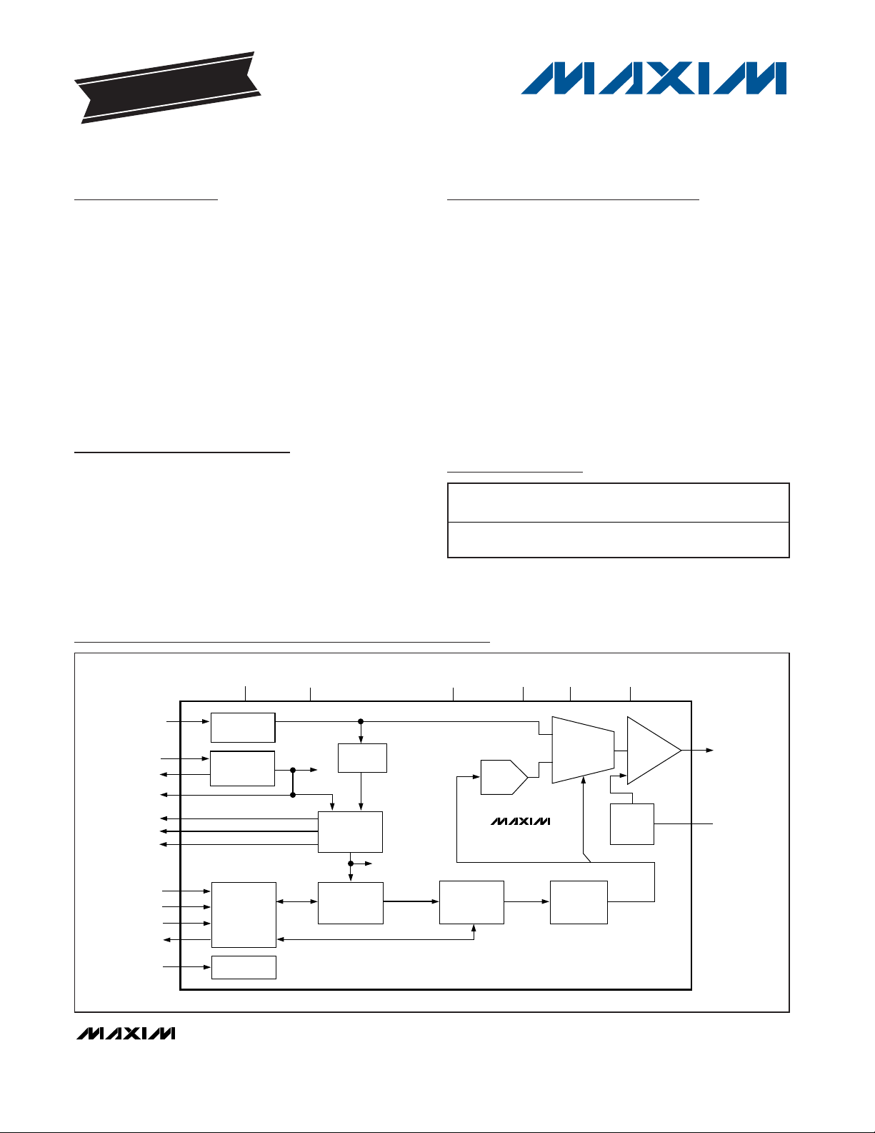
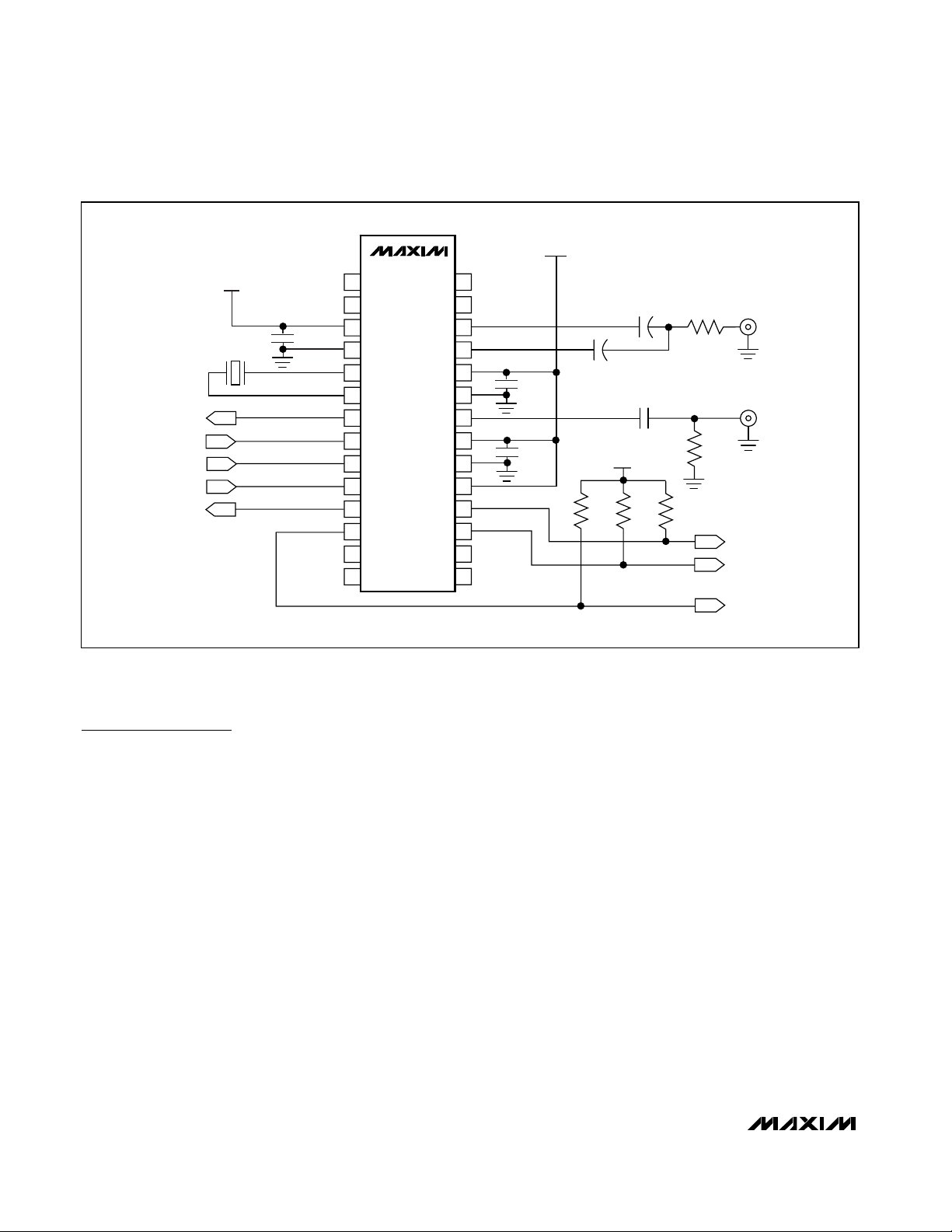
SERIAL
INTERFACE
DISPLAY
ADDRESS
VIDEO
DRIVER
VIDEO
TIMING
GENERATOR
DISPLAY
MEMORY
(SRAMS)
CHARACTER
ADDRESS
PIXEL
CODE
SYNC
PIXEL
CONTROL
CHARACTER
MEMORY
(NVM)
OSD
GENERATOR
SAG
NETWORK
OSD
MUX
DAC
SYSTEM
CLOCK
POR
SYNC
SEPARATOR
XTAL
OSCILLATOR
CLAMP
VIN
CLKIN
XFB
CLKOUT
RESET
HSYNC
VSYNC
LOS
CS
SCLK
SDIN
SDOUT
AVDD
AGND
DVDD
DGND
PVDD
PGND
VOUT
SAG
MAX7456
Simplified Functional Diagram
SPI is a trademark of Motorola, Inc.
EVALUATION KIT
AVAILABLE
PIN-PACKAGE LANGUAGE
28 TSSOP-EP*
MAX7456
Single-Channel Monochrome On-Screen
Display with Integrated EEPROM
2 _______________________________________________________________________________________
ABSOLUTE MAXIMUM RATINGS
Stresses beyond those listed under “Absolute Maximum Ratings” may cause permanent damage to the device. These are stress ratings only, and functional
operation of the device at these or any other conditions beyond those indicated in the operational sections of the specifications is not implied. Exposure to
absolute maximum rating conditions for extended periods may affect device reliability.
AVDD to AGND ........................................................-0.3V to +6V
DVDD to DGND ........................................................-0.3V to +6V
PVDD to PGND.........................................................-0.3V to +6V
AGND to DGND.....................................................-0.3V to +0.3V
AGND to PGND .....................................................-0.3V to +0.3V
DGND to PGND.....................................................-0.3V to +0.3V
VIN, VOUT, SAG to AGND......................-0.3V to (V
AVDD
+ 0.3V)
HSYNC, VSYNC, LOS to AGND ...............................-0.3V to +6V
RESET to AGND .....................................-0.3V to (V
AVDD
+ 0.3V)
CLKIN, CLKOUT, XFB to DGND ............-0.3V to (V
DVDD
+ 0.3V)
SDIN, SCLK, CS, SDOUT to DGND........-0.3V to (V
DVDD
+ 0.3V)
Maximum Continuous Current into V
OUT
........................±100mA
Continuous Power Dissipation (T
A
= +70°C)
28-Pin TSSOP (derate 27mW/°C above +70°C).......2162mW*
Operating Temperature Range ...........................-40°C to +85°C
Junction Temperature......................................................+150°C
Storage Temperature Range .............................-60°C to +150°C
Lead Temperature (soldering, 10s) .................................+300°C
ELECTRICAL CHARACTERISTICS
(V
AVDD
= +4.75V to +5.25V, V
DVDD
= +4.75V to +5.25V, V
PVDD
= +4.75V to +5.25V, TA= T
MIN
to T
MAX
. Typical values are at V
AVDD
= V
DVDD
= V
PVDD
= +5V, TA= +25°C, unless otherwise noted.) (Note 1)
PARAMETER
CONDITIONS MIN
UNITS
POWER SUPPLIES
Analog Supply Voltage V
AVDD
5 5.25 V
Digital Supply Voltage V
DVDD
5 5.25 V
Driver Supply Voltage V
PVDD
5 5.25 V
Analog Supply Current I
AVDD
VIN = 1V
P-P
(100% white flat field signal),
VOUT load, R
L
= 150Ω
24 35 mA
Digital Supply Current I
DVDD
VIN = 1V
P-P
(100% white flat field signal),
VOUT load, R
L
= 150Ω
25 30 mA
Driver Supply Current I
PVDD
VIN = 1V
P-P
(100% white flat field signal),
VOUT load, R
L
= 150Ω
58 80 mA
NONVOLATILE MEMORY
Data Retention TA = +25°C 100 Years
Endurance TA = +25°C
Stores
DIGITAL INPUTS (CS, SDIN, RESET, SCLK)
Input High Voltage V
IH
2.0 V
Input Low Voltage V
IL
0.8 V
Input Hysteresis V
HYS
50 mV
Input Leakage Current VIN = 0 or V
DVDD
±10 µA
Input Capacitance C
IN
5pF
DIGITAL OUTPUTS (SDOUT, CLKOUT, VSYNC, HSYNC, LOS)
Output High Voltage V
OH
I
SOURCE
= 4mA (SDOUT, CLKOUT) 2.4 V
Output Low Voltage V
OL
I
SINK
= 4mA 0.45 V
Tri-State Leakage Current SDOUT, CS = V
DVDD
±10 µA
*As per JEDEC51 Standard (Multilayer Board).
SYMBOL
TYP MAX
4.75
4.75
4.75
100,000
MAX7456
Single-Channel Monochrome On-Screen
Display with Integrated EEPROM
_______________________________________________________________________________________ 3
ELECTRICAL CHARACTERISTICS (continued)
(V
AVDD
= +4.75V to +5.25V, V
DVDD
= +4.75V to +5.25V, V
PVDD
= +4.75V to +5.25V, TA= T
MIN
to T
MAX
. Typical values are at V
AVDD
= V
DVDD
= V
PVDD
= +5V, TA= +25°C, unless otherwise noted.) (Note 1)
PARAMETER
SYMBOL
CONDITIONS MIN
TYP
MAX
UNITS
CLOCK INPUT (CLKIN)
Clock Frequency 27 MHz
Clock-Pulse High 14 ns
Clock-Pulse Low 14 ns
Input High Voltage
0.7 x
V
Input Low Voltage
0.3 x
V
Input Leakage Current VIN = 0V or V
DVDD
±50 µA
CLOCK OUTPUT (CLKOUT)
Duty Cycle 5pF and 10kΩ to DGND 40 50 60 %
Rise Time 5pF and 10kΩ to DGND 3 ns
Fall Time 5pF and 10kΩ to DGND 3 ns
VIDEO CHARACTERISTICS
DC Power-Supply Rejection
V
AVDD
= V
DVDD
= V
PVDD
= 5V;
V
IN
= 1V
P-P
, measured at VOUT
40 dB
AC Power-Supply Rejection
V
AVDD
= V
DVDD
= V
PVDD
= 5V;
V
IN
= 1V
P-P
, measured at VOUT;
f = 5MHz; power-supply ripple = 0.2V
P-P
30 dB
Short-Circuit Current VOUT to PGND 230 mA
Line-Time Distortion LTD Figures 1a, 1b 0.5 %
Output Impedance Z
OUT
Figures 1a, 1b 0.2 Ω
Gain Figures 1a, 1b
2.0 2.11 V/V
Black Level At VOUT, Figures 1a, 1b
AGND
V
Input-Voltage Operating Range
V
IN
Figures 1a, 3 (Note 2) 0.5 1.2 V
P-P
Input-Voltage Sync Detection
Range
V
INSD
Figures 1a, 3 (Note 3) 0.5 2.0 V
P-P
Maximum Output-Voltage Swing
V
OUT
Figures 1a, 1b 2.4 V
P-P
Output-Voltage Sync Tip Level 0.7 V
Large Signal Bandwidth (0.2dB)
BW V
OUT
= 2V
P-P
, Figures 1a, 1b 6 MHz
VIN to VOUT Delay 30 ns
Differential Gain DG 0.5 %
Differential Phase DP 0.5
Degrees
OSD White Level
VOUT 100% white level with respect to
black level
1.45 V
Horizontal Pixel Jitter Between consecutive horizontal lines 24 ns
Video Clamp Settling Time 32 Lines
V
DVDD
1.89
V
DVDD
+ 1.5
1.25 1.33
MAX7456
Single-Channel Monochrome On-Screen
Display with Integrated EEPROM
4 _______________________________________________________________________________________
TIMING CHARACTERISTICS
(V
AVDD
= +4.75V to +5.25V, V
DVDD
= +4.75V to +5.25V, V
PVDD
= +4.75V to +5.25V, TA= T
MIN
to T
MAX
. Typical values are at V
AVDD
= V
DVDD
= V
PVDD
= +5V, TA= +25°C, unless otherwise noted.) (Note 1)
PARAMETER
CONDITIONS MIN
UNITS
SPI TIMING
SCLK Period t
CP
100 ns
SCLK Pulse-Width High t
CH
40 ns
SCLK Pulse-Width Low t
CL
40 ns
CS Fall to SCLK Rise Setup t
CSS0
30 ns
CS Fall After SCLK Rise Hold t
CSH0
0ns
CS Rise to SCLK Setup t
CSS1
30 ns
CS Rise After SCLK Hold t
CSH1
0ns
CS Pulse-Width High t
CSW
100 ns
SDIN to SCLK Setup t
DS
30 ns
SDIN to SCLK Hold t
DH
0ns
SDOUT Valid Before SCLK t
DO1
20pF to ground 25 ns
SDOUT Valid After SCLK t
DO2
20pF to ground 0 ns
CS High to SDOUT High
Impedance
t
DO3
20pF to ground 300 ns
CS Low to SDOUT Logic Level t
DO4
20pF to ground 20 ns
HSYNC, VSYNC, AND LOS TIMING
LOS, VSYNC, and HSYNC Valid
before CLKOUT Rising Edge
t
DOV
20pF to ground 30 ns
NTSC external sync mode, Figure 4 375
VOUT Sync to VSYNC Falling
Edge Delay
PAL external sync mode, Figure 6 400
ns
ELECTRICAL CHARACTERISTICS (continued)
(V
AVDD
= +4.75V to +5.25V, V
DVDD
= +4.75V to +5.25V, V
PVDD
= +4.75V to +5.25V, TA= T
MIN
to T
MAX
. Typical values are at V
AVDD
= V
DVDD
= V
PVDD
= +5V, TA= +25°C, unless otherwise noted.) (Note 1)
PARAMETER
SYMBOL
CONDITIONS MIN
TYP
MAX
UNITS
OSD CHARACTERISTICS
OSD Rise Time
OSD insertion mux register
OSDM[5,4,3] = 011b
60 ns
OSD Fall Time
OSD insertion mux register
OSDM[5,4,3] = 011b
60 ns
OSD insertion mux register
OSDM[2,1,0] = 011b
75 ns
OSD Insertion Mux Switch Time
SYMBOL
TYP MAX
t
VOUT-VSF
MAX7456
Single-Channel Monochrome On-Screen
Display with Integrated EEPROM
_______________________________________________________________________________________ 5
Note 1: See the standard test circuits of Figure 1. RL= 75Ω, unless otherwise specified. All digital input signals are timed from a
voltage level of (V
IH
+ VIL) / 2. All parameters are tested at TA= +85°C and values through temperature range are guaran-
teed by design.
Note 2: The input-voltage operating range is the input range over which the output signal parameters are guaranteed (Figure 3).
Note 3: The input-voltage sync detection range is the input composite video range over which an input sync signal is properly
detected and the OSD signal appears at VOUT. However, the output voltage specifications are not guaranteed for input signals exceeding the maximum specified in the input operating voltage range (Figure 3).
TIMING CHARACTERISTICS (continued)
(V
AVDD
= +4.75V to +5.25V, V
DVDD
= +4.75V to +5.25V, V
PVDD
= +4.75V to +5.25V, TA= T
MIN
to T
MAX
. Typical values are at V
AVDD
= V
DVDD
= V
PVDD
= +5V, TA= +25°C, unless otherwise noted.) (Note 1)
PARAMETER
CONDITIONS MIN
UNITS
NTSC external sync mode, Figure 4 400
VOUT Sync to VSYNC Rising
Edge Delay
PAL external sync mode, Figure 6 425
ns
NTSC internal sync mode, Figure 5 40
VSYNC Falling Edge to VOUT
Sync Delay
PAL internal sync mode, Figure 7 45
ns
NTSC internal sync mode, Figure 5 32
VSYNC Rising Edge to VOUT
Sync Delay
PAL internal sync mode, Figure 7 30
ns
VOUT Sync to HSYNC Falling
Edge Delay
NTSC and PAL external sync mode,
Figure 8
310 ns
VOUT Sync to HSYNC Rising
Edge Delay
NTSC and PAL external sync mode,
Figure 8
325 ns
HSYNC Falling Edge to VOUT
Sync Delay
NTSC and PAL internal sync mode,
Figure 9
115 ns
HSYNC Rising Edge to VOUT
Sync Delay
NTSC and PAL internal sync mode,
Figure 9
115 ns
All Supplies High to CS Low t
PUD
Power-up delay 50 ms
NVM Write Busy t
NVW
12 ms
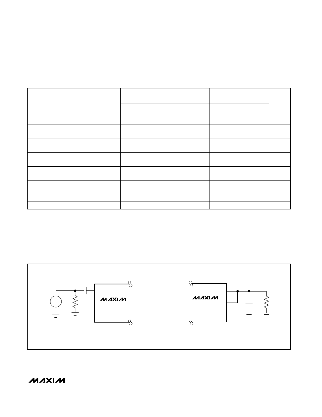
Figure 1. Standard Test Circuits
SYMBOL
t
VOUT-VSR
t
VSF-VOUT
t
VSR-VOUT
t
VOUT-HSF
t
VOUT-HSR
t
HSF-VOUT
t
HSR-VOUT
TYP MAX
SIGNAL
GEN
R
75Ω
IN
C
IN
0.1µF
VIN
a) INPUT TEST CIRCUIT
MAX7456
VOUT
C
MAX7456
SAG
L
22pF
b) ONE STANDARD VIDEO LOAD, DC-COUPLED
R
L
150Ω
MAX7456
Single-Channel Monochrome On-Screen
Display with Integrated EEPROM
6 _______________________________________________________________________________________
IMAGE WITH ON-SCREEN GRAPHICS
MAX7456 toc01
10µs/div
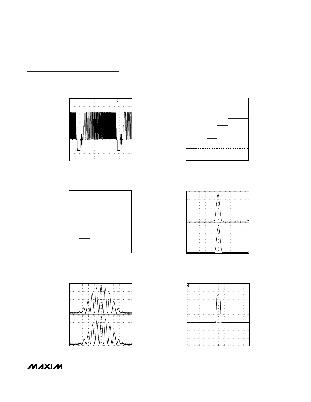
100% COLOR BARS RESPONSE
CVBS OUT
(200mV/div)
MAX7456 toc02
75% COLOR BARS VECTOR DIAGRAM
CVBS OUT
MAX7456 toc03
10µs/div
60% MULTIBURST RESPONSE
CVBS OUT
(200mV/div)
MAX7456 toc04
Typical Operating Characteristics
(V
AVDD
= +5V, V
DVDD
= +5V, V
PVDD
= +5V, TA= +25°C, unless otherwise noted. See the Typical Operating Circuit of Figure 2, if applicable.)
MAX7456
Single-Channel Monochrome On-Screen
Display with Integrated EEPROM
_______________________________________________________________________________________ 7
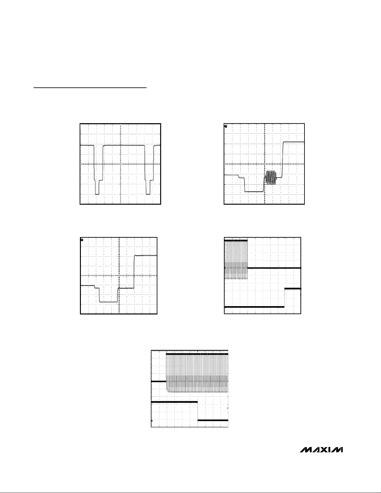
10µs/div
100% SWEEP RESPONSE
CVBS OUT
(200mV/div)
MAX7456 toc05
DIFFERENTIAL PHASE
MAX7456 toc06
STEP
DIFFERENTIAL PHASE (deg)
6th5th4th3rd2nd1st
0
0.05
0.10
CVBS OUT
0.15
0.20
-0.05
DIFFERENTIAL GAIN
MAX7456 toc07
STEP
DIFFERENTIAL GAIN (%)
6th5th4th3rd2nd1st
0
0.05
0.10
0.15
0.20
-0.05
CVBS OUT
400ns/div
2T RESPONSE
CVBS IN
(200mV/div)
CVBS OUT
(200mV/div)
MAX7456 toc08
400ns/div
12.5T RESPONSE
CVBS IN
(200mV/div)
CVBS OUT
(200mV/div)
MAX7456 toc09
200ns/div
OSD OUTPUT 100% WHITE PIXEL
CVBS OUT
(200mV/div)
MAX7456 toc10
Typical Operating Characteristics (continued)
(V
AVDD
= +5V, V
DVDD
= +5V, V
PVDD
= +5V, TA= +25°C, unless otherwise noted. See the Typical Operating Circuit of Figure 2, if applicable.)
MAX7456
Single-Channel Monochrome On-Screen
Display with Integrated EEPROM
8 _______________________________________________________________________________________
Typical Operating Characteristics (continued)
(V
AVDD
= +5V, V
DVDD
= +5V, V
PVDD
= +5V, TA= +25°C, unless otherwise noted. See the Typical Operating Circuit of Figure 2, if applicable.)
10µs/div
LINE-TIME DISTORTION
CVBS OUT
(200mV/div)
MAX7456 toc11
2µs/div
H TIMING (EXTERNAL-SYNC MODE)
CVBS OUT
(200mV/div)
MAX7456 toc12
2µs/div
H TIMING (INTERNAL-SYNC MODE)
CVBS OUT
(200mV/div)
MAX7456 toc13
500µs/div
LOSS-OF-SYNC (LOW TO HIGH)
CVBS OUT
(200mV/div)
LOS
(1V/div)
MAX7456 toc14
500µs/div
LOSS-OF-SYNC (HIGH TO LOW)
CVBS OUT
(200mV/div)
LOS
(1V/div)
MAX7456 toc15
MAX7456
Single-Channel Monochrome On-Screen
Display with Integrated EEPROM
_______________________________________________________________________________________ 9
Pin Description
PIN NAME FUNCTION
1, 2, 13–16,
27, 28
N.C. No Connection. Not internally connected.
3 DVDD Digital Power-Supply Input. Bypass to DGND with a 0.1µF capacitor.
4 DGND Digital Ground
5 CLKIN
Crystal Connection 1. Connect a parallel resonant, fundamental mode crystal between CLKIN and XFB
for use as a crystal oscillator, or drive CLKIN directly with a 27MHz system reference clock.
6 XFB
Crystal Connection 2. Connect a parallel resonant, fundamental mode crystal between CLKIN and XFB
for use as a crystal oscillator, or leave XFB unconnected when driving CLKIN with a 27MHz system
reference clock.
7
Clock Output. 27MHz logic-level output system clock.
8 CS Active-Low Chip-Select Input. SDOUT goes high impedance when CS is high.
9 SDIN Serial Data Input. Data is clocked in at rising edge of SCLK.
10 SCLK
Serial Clock Input. Clocks data into SDIN and out of SDOUT. Duty cycle must be between 40% and 60%.
11
Serial Data Output. Data is clocked out at the falling edge of SCLK. High impedance when CS is high.
12 LOS
Loss-of-Sync Output (Open-Drain). LOS goes high when the VIN sync pulse is lost for 32 consecutive
lines. LOS goes low when 32 consecutive valid sync pulses are received. Connect to a 1kΩ pullup
resistor to DVDD or another positive supply voltage suitable for the receiving device.
17
Vertical Sync Output (Open-Drain). VSYNC goes low following the video input’s vertical sync interval.
VSYNC is either recovered from VIN or internally generated when in internal sync mode. Connect to a
1kΩ pullup resistor to DVDD or another positive supply voltage suitable for the receiving device.
18
Horizontal Sync Output (Open-Drain). HSYNC goes low following the video input’s horizontal sync
interval. HSYNC is either recovered from VIN or internally generated when in internal sync mode. Connect
to a 1kΩ pullup resistor to DVDD or another positive supply voltage suitable for the receiving device.
19
System Reset Input. The minimum RESET pulse width is 50ms. All SPI registers are reset to their default
values after 100µs following the rising edge of RESET. These registers are not accessible for reading or
writing during that time. The display memory is reset to its default value of 00H in all locations after 20µs
following the rising edge of RESET.
20 AGND Analog Ground
21 AVDD Analog Power-Supply Input. Bypass to AGND with a 0.1µF capacitor.
22 VIN PAL or NTSC CVBS Video Input
23 PGND Driver Ground. Connect to AGND at a single point.
24 PVDD Driver Power-Supply Input. Bypass to PGND with a 0.1µF capacitor.
25 SAG Sag Correction Input. Connect to VOUT if not used. See Figure 1b.
26 VOUT Video Output
—EP
Exposed Pad. Internally connected to AGND. Connect EP to the AGND plane for improved heat
dissipation. Do not use EP as the only ground connection.
CLKOUT
SDOUT
VSYNC
HSYNC
RESET
MAX7456
Single-Channel Monochrome On-Screen
Display with Integrated EEPROM
10 ______________________________________________________________________________________
Detailed Description
The MAX7456 single-channel monochrome on-screen
display (OSD) generator integrates all the functions needed to generate a user-defined OSD and insert it into the
output signal. The MAX7456 accepts a composite NTSC
or PAL video signal. The device includes an input clamp,
sync separator, video timing generator, OSD insertion
mux, nonvolatile character memory, display memory,
OSD generator, crystal oscillator, an SPI-compatible interface to read/write the OSD data, and a video driver (see
the Simplified Functional Diagram). Additionally, the
MAX7456 provides vertical sync (VSYNC), horizontal
sync (HSYNC), and loss-of sync (LOS) outputs for system
synchronization. A clock output signal (CLKOUT) allows
daisy-chaining of multiple devices.
See the MAX7456 Register Description section for an
explanation of register notation use in this data sheet.
The 256 user-defined 12 x 18 pixel character set
comes preloaded and is combined with the input video
stream to generate a CVBS signal with OSD video output. A maximum of 256 12 x 18 pixel characters can be
reprogrammed in the NVM. In NTSC mode, 13 rows x
30 characters are displayed. In PAL mode, 16 rows x
30 characters are displayed. When the input video signal is absent, the OSD image can still be displayed by
using the MAX7456’s internal video timing generator.
Video Input
The MAX7456 accepts standard NTSC or PAL CVBS
signals at VIN. The video signal input must be AC-coupled with a 0.1µF capacitor and is internally clamped.
An input coupling capacitance of 0.1µF is required to
guarantee the specified line-time distortion (LTD) and
video clamp settling time. The video clamp settling time
changes proportionally to the input coupling capacitance, and LTD changes inversely proportional to the
capacitance.
28
27
26
25
24
23
22
21
20
19
18
17
16
15
1
2
3
4
5
6
7
8
9
10
11
12
13
14
MAX7456
SDIN
+5V
27MHz
SDOUT
+5V
CVBS OUT
SAG
PGND
RESET
HSYNC
VSYNC
DGND
CLKIN
XFB
CLKOUT
CS
SDIN
SCLK
SDOUT
LOS
N.C.
SCLK
CS
CVBS IN
LOS
VS
HS
N.C.
N.C.
N.C.
CLKOUT
N.C.
N.C.
AGND
N.C.
N.C.
+5V
0.1µF
C
OUT
75Ω
75Ω
1kΩ1kΩ1kΩ
0.1µF
0.1µF
0.1µF
C
SAG
DVDD
VOUT
PVDD
VIN
AVDD
Figure 2. Typical Operating Circuit
MAX7456
Single-Channel Monochrome On-Screen
Display with Integrated EEPROM
______________________________________________________________________________________ 11
Input Clamp
The MAX7456’s clamp is a DC-restore circuit that uses
the input coupling capacitor to correct any DC shift of
the input signal, on a line-by-line basis, such that the
sync tip at VIN is approximately 550mV. This establishes a DC level at VIN suitable for the on-chip sync
detection and video processing functions. This circuitry
also removes low-frequency noise such as 60Hz hum
or other additive low-frequency noise.
Sync Separator
The sync separator detects the composite sync pulses
on the video input and extracts the timing information to
generate HSYNC and VSYNC. It is also used for internal OSD synchronization and loss-of-sync (LOS) detection. LOS goes high if no sync signal is detected at VIN
for 32 consecutive lines, and goes low if 32 consecutive horizontal sync signals are detected. During a LOS
condition, when VM0[5] = 0 (Video Mode 0 register, bit
5), only the OSD appears at the VOUT. At this time, the
input image is set to a gray level at VOUT as determined by VM1[6:4]. The behavior of all sync modes is
shown in Table 1.
COLOR BURST
SYNC TIP
LEVEL
BLACK LEVEL
WHITE LEVEL
MAXIMUM VIDEO SWING
INPUT VOLTAGE
MINIMUM VIDEO SWING
VIN
Figure 3. Definition of Terms
VIDEO MODE VIN VSYNC HSYNC LOS VOUT
Video Active Active Low VIN + OSD
Auto Sync Select Mode
VM0[5, 4] = 0x
No input Active Active High OSD only
Video Active Active Low VIN + OSD
External Sync Select
VM0[5, 4] = 10
No input Inactive (high) Inactive (high) High DC
Video Active Active High OSD only
Internal Sync Select
VM0[5, 4] = 11
No input Active Active High OSD only
Table 1. Video Sync Modes
X = Don’t care.
MAX7456
Single-Channel Monochrome On-Screen
Display with Integrated EEPROM
12 ______________________________________________________________________________________
Video Timing Generator
The video timing generator is a digital circuit generating all internal and external (VSYNC and HSYNC) timing signals. VSYNC and HSYNC can be synchronized
to VIN, or run independently of any input when in internal sync mode. The video timing generator can generate NTSC or PAL timing using the same 27MHz crystal
(see Figures 4–9).
Crystal Oscillator
The internal crystal oscillator generates the system
clock used by the video timing generator. The oscillator
uses a 27MHz crystal or can be driven by an external
27MHz TTL clock at CLKIN. For external clock mode,
connect the 27MHz TTL input clock to CLKIN and leave
XFB unconnected.
Display Memory (SRAM)
The display memory stores 480 character addresses
that point to the characters stored in the NVM character
memory. The content of the display memory is userprogrammable through the SPI-compatible serial interface. The display-memory address corresponds to a
fixed location on a monitor (see Figure 10). Momentary
breakup of the OSD image can be prevented by writing
to the display memory during the vertical blanking interval. This can be achieved by using VSYNC as an interrupt to the host processor to initiate writing to the
display memory.
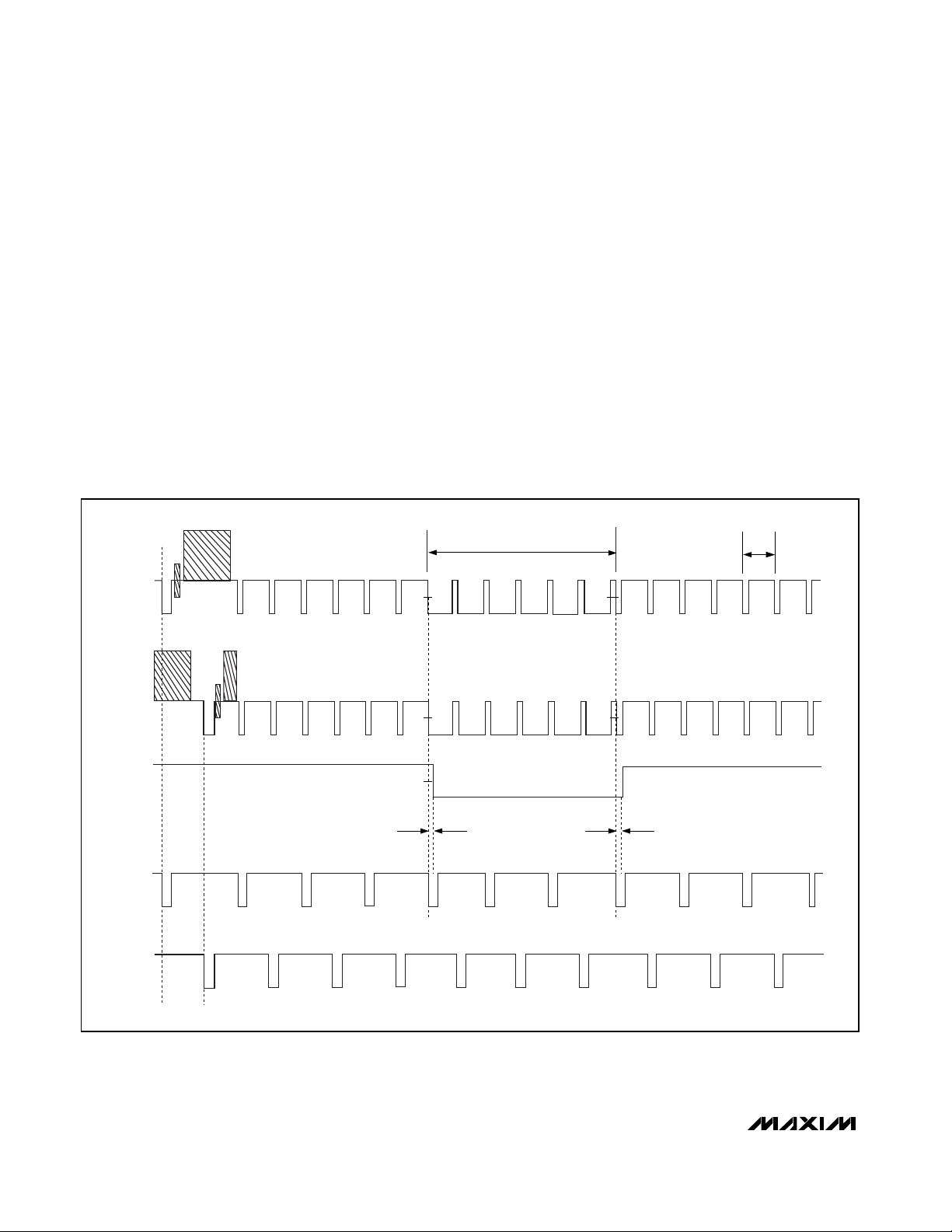
t
VOUT-VSF
1/2H
VERTICAL SYNCHRONIZATION
PULSE INTERVAL
VOUT
(ODD FIELD)
VOUT
(EVEN FIELD)
VSYNC
HSYNC
(ODD FIELD)
HSYNC
(EVEN FIELD)
50%
50%
t
VOUT-VSR
50%
50%
50%
Figure 4. VOUT,
VSYNC
, and
HSYNC
Timing (NTSC, External Sync Mode)
MAX7456
Single-Channel Monochrome On-Screen
Display with Integrated EEPROM
______________________________________________________________________________________ 13
t
VSF-VOUT
1/2H
VERTICAL SYNCHRONIZATION
PULSE INTERVAL
VOUT
(ODD FIELD)
VOUT
(EVEN FIELD)
VSYNC
HSYNC
(ODD FIELD)
HSYNC
(EVEN FIELD)
50%
50%
t
VSR-VOUT
50%
50%
50%
50%
Figure 5. VOUT,
VSYNC
, and
HSYNC
Timing (NTSC, Internal Sync Mode)

MAX7456
Single-Channel Monochrome On-Screen
Display with Integrated EEPROM
14 ______________________________________________________________________________________
t
VOUT-VSF
t
VOUT-VSR
1/2H
VERTICAL SYNCHRONIZATION
PULSE INTERVAL
VOUT
(ODD FIELD)
VOUT
(EVEN FIELD)
VSYNC
HSYNC
(ODD FIELD)
HSYNC
(EVEN FIELD)
50%
50%
50% 50%
50%
50%
Figure 6. VOUT,
VSYNC
, and
HSYNC
Timing (PAL, External Sync Mode)

MAX7456
Single-Channel Monochrome On-Screen
Display with Integrated EEPROM
______________________________________________________________________________________ 15
t
VSF-VOUT
t
VSR-VOUT
1/2H
VERTICAL SYNCHRONIZATION
PULSE INTERVAL
VOUT
(ODD FIELD)
VOUT
(EVEN FIELD)
VSYNC
HSYNC
(ODD FIELD)
HSYNC
(EVEN FIELD)
50%
50%
50% 50%
50%
50%
Figure 7. VOUT,
VSYNC
, and
HSYNC
Timing (PAL, Internal Sync Mode)

MAX7456
Single-Channel Monochrome On-Screen
Display with Integrated EEPROM
16 ______________________________________________________________________________________
VOUT
HSYNC
t
VOUT-HSF
t
VOUT-HSR
50%50%
Figure 8. VOUT, and
HSYNC
Horizontal Sync Timing (NTSC and PAL, External Sync Mode)
VOUT
HSYNC
t
HSF-VOUT
t
HSR-VOUT
50%
50%
Figure 9. VOUT and
HSYNC
Horizontal Sync Timing (NTSC and PAL, Internal Sync Mode)

Character Memory (NVM)
The character memory is a 256-row x 64-byte wide
nonvolatile memory (NVM) that stores the characters or
graphic images, and is factory preloaded with the characters shown in Figure 12. The content of the character
memory is user-programmable through the SPI-compatible serial interface. Each row contains the description of a single OSD character. Each character consists
of 12 horizontal x 18 vertical pixels where each pixel is
represented by 2 bits of data having three states: white,
black, or transparent. Thus, each character requires 54
bytes of pixel data (Figure 11).
The NVM requires reading and writing a whole character (64 bytes) at a time. This is enabled by an additional
row of memory called the shadow RAM. The 64-byte
temporary shadow RAM contains all the pixel data of a
selected character (CMAH[7:0]) and is used as a buffer
for read and write operations to the NVM (Figure 13).
Accessing the NVM is always through the shadow
RAM, and is thus a two-step process. To write a character to the NVM, the user first fills the shadow RAM
using 54 8-bit SPI write operations, and then executes
a single shadow RAM write command. Similarly, reading a character’s pixel values requires first reading a
character’s pixel data into the shadow RAM, and then
reading the desired pixel data from the shadow RAM to
the SPI port.
MAX7456
Single-Channel Monochrome On-Screen
Display with Integrated EEPROM
______________________________________________________________________________________ 17
DISPLAY MEMORY
(TWO, 256 x 16-BIT SRAMs)
0
ADDRESS (8 BIT)
L
B
C
L
B
C
B
L
K
B
L
K
I
N
V
I
N
V
L
B
C
B
L
K
I
N
V
479
29
DISPLAY AREA
(16 ROWS x 30 CHARACTERS)
0
29
450 479
CHARACTER ATTRIBUTE BIT DEFINITIONS:
LBC = LOCAL BACKGROUND CONTROL
BLK = BLINK CONTROL
INV = INVERT CONTROL
X = DON'T CARE
CHARACTER MEMORY
ADDRESS LOW (CMAL)
0
PIXEL DATA ARRANGEMENT IN CHARACTER MEMORY (NVM)
256 ROWS x 64 BYTES EEPROM
0 1 2 515253 6162 63
012
51 52 53 61 62 63
12 PIXELS
4 PIXEL VALUES
(1 BYTE)
(SEE FIGURE 11 FOR PIXEL MAP)
CHARACTER
DATA USAGE
(12 x 18 PIXELS)
012
51 52 53
18 PIXELS
2-BIT PIXEL DEFINITIONS:
00 = BLACK, OPAQUE
10 = WHITE, OPAQUE
X1 = TRANSPARENT (EXTERNAL SYNC MODE)
OR GRAY (INTERNAL SYNC MODE)
DISPLAY MEMORY ADDRESS
(DMAH, DMAL)
DISPLAY MEMORY ADDRESS
(DMAH, DMAL)
ADDRESS (8 BIT)
ADDRESS (8 BIT)
30
59
UNUSED
MEMORY
X
XXXX
X
XXXX
X
XXXX
CHARACTER
ADDRESS (CA)
CHARACTER
ATTRIBUTE
255
0
54
54
53
54
CHARACTER
DATA
CHARACTER MEMORY
ADDRESS HIGH (CMAH)
CHARACTER DATA
ARRANGEMENT IN
DISPLAY MEMORY
(SRAM) 480 ROWS
x 2 BYTES SRAM
63
Figure 10. Definitions of Various Parameters

MAX7456
Single-Channel Monochrome On-Screen
Display with Integrated EEPROM
18 ______________________________________________________________________________________
0 0, 1, 2
1 3, 4, 5
2 6, 7, 8
3 9, 10, 11
4 12, 13, 14
5 15, 16, 17
6 18, 19, 20
7 21, 22, 23
8 24, 25, 26
9 27, 28, 29
10 30, 31, 32
11 33, 34, 35
12 36, 37, 38
13 39, 40, 41
14 42, 43, 44
15 45, 46, 47
16 48, 49, 50
17 51, 52, 53
00 = BLACK
CHARACTER MEMORY
ADDRESS LOW
CMAL[5:0]
2-BIT PIXEL DEFINITION:
[5, 4] [3, 2]
10 = WHITE
X = DON'T CARE
X1 = TRANSPARENT (EXTERNAL SYNC MODE)
OR GRAY (INTERNAL SYNC MODE)
[x, y]
[x, y]
7
[7, 6] [5, 4] [3, 2]
[7, 6] [5, 4]
[7, 6]
[x, y]
PIXEL COLUMN NUMBER
PIXEL ROW NUMBER
[1, 0][5, 4] [3, 2]
[1, 0] [7, 6]
0
CDMI
[5, 4]
CDMI
[3, 2]
123456
CDMI
[7, 6]
CDMI
[1, 0]
[7, 6]
8 9 10 11
[5, 4] [3, 2]
[7, 6] [5, 4] [3, 2]
[7, 6] [5, 4] [3, 2]
[7, 6] [5, 4] [3, 2] [1, 0]
[7, 6] [5, 4] [3, 2] [1, 0]
[5, 4] [3, 2] [1, 0]
[1, 0]
[5, 4] [3, 2] [1, 0][7, 6]
[1, 0] [7, 6] [5, 4] [3, 2] [1, 0] [7, 6]
[7, 6] [5, 4]
[7, 6] [5, 4] [3, 2]
[7, 6] [5, 4] [3, 2] [1, 0]
[1, 0]
[3, 2] [1, 0] [7, 6] [5, 4]
[7, 6] [5, 4] [3, 2] [1, 0][7, 6] [5, 4] [3, 2] [1, 0]
[5, 4] [3, 2] [1, 0]
[1, 0][5, 4] [3, 2]
[1, 0]
[7, 6] [5, 4] [3, 2] [1, 0] [7, 6] [5, 4]
[7, 6] [5, 4]
[3, 2] [1, 0] [7, 6] [5, 4]
[1, 0] [3, 2] [1, 0]
[7, 6] [5, 4] [3, 2] [1, 0] [7, 6] [5, 4] [3, 2] [1, 0]
[5, 4] [3, 2] [1, 0]
[1, 0] [7, 6] [5, 4] [3, 2] [1, 0] [7, 6] [5, 4] [3, 2] [1, 0]
[7, 6] [5, 4] [3, 2] [1, 0] [7, 6] [5, 4] [3, 2] [1, 0]
[1, 0] [5, 4] [3, 2] [1, 0][7, 6] [7, 6]
[7, 6] [5, 4] [3, 2] [1, 0] [7, 6] [5, 4] [3, 2] [1, 0] [7, 6] [5, 4] [3, 2] [1, 0]
[7, 6] [5, 4] [3, 2] [1, 0]
[1, 0]
[7, 6] [5, 4]
[3, 2]
[7, 6] [5, 4] [3, 2]
[5, 4] [3, 2]
[5, 4]
[3, 2] [1, 0] [7, 6]
[7, 6] [5, 4] [3, 2] [1, 0]
[1, 0]
[1, 0]
[3, 2] [1, 0] [7, 6] [5, 4] [3, 2] [1, 0]
[1, 0] [7, 6][7, 6] [5, 4] [3, 2]
[7, 6][7, 6] [5, 4] [3, 2] [1, 0]
[3, 2]
[5, 4] [3, 2]
[1, 0]
[1, 0]
[7, 6] [5, 4] [3, 2] [1, 0] [7, 6] [5, 4] [3, 2] [1, 0]
[7, 6] [5, 4] [3, 2]
[7, 6]
[7, 6]
[5, 4] [3, 2] [1, 0] [7, 6] [5, 4] [3, 2] [1, 0] [7, 6]
[3, 2] [1, 0]
[7, 6] [5, 4] [3, 2] [1, 0] [7, 6] [5, 4] [3, 2]
[3, 2] [1, 0] [7, 6] [5, 4]
Figure 11. Character Data Usage (Pixel Map)

MAX7456
Single-Channel Monochrome On-Screen
Display with Integrated EEPROM
______________________________________________________________________________________ 19
CA[3:0], CMAH[3:0]
CA[7:4], CMAH[7:4]
Figure 12. Character Address Map (Default Character Set)

MAX7456
On-Screen Display (OSD) Generator
The OSD generator sets each pixel amplitude based on
the content of the character memory and Row
Brightness registers (RB0–RB15).
OSD Insertion Mux
The OSD insertion mux selects between an OSD pixel
and the input video signal. The OSD image sharpness
is controlled by the OSD Rise and Fall Time bits, and
the OSD Insertion Mux Switching Time bits, found in the
OSD Insertion Mux (OSDM) register. This register controls the trade-off between OSD image sharpness and
crosscolor/crossluma artifacts. Lower time settings produce sharper pixels, but potentially greater crosscolor/crossluma artifacts. The optimum setting depends
on the requirements of the application and, therefore,
can be set by the user.
Video-Driver Output
The MAX7456 includes a video-driver output with a
gain of 2. The driver has a maximum of 2.4V
P-P
output
swing and a 6MHz large signal bandwidth (≤ 0.2dB
attenuation). The driver output is capable of driving two
150Ω standard video loads.
Sag Correction
Sag correction is a means of reducing the electrical
and physical size of the output coupling capacitor while
achieving acceptable line-time distortion. Sag correction refers to the low frequency compensation of the
highpass filter formed by the 150Ω load of a back-ter-
minated coaxial cable and the output coupling capacitor. This breakpoint must be low enough in frequency to
pass the vertical sync interval (< 25Hz for PAL and
< 30Hz for NTSC) to avoid field tilt. Traditionally, the
breakpoint is made < 5Hz, and the coupling capacitor
must be very large, typically > 330µF. The MAX7456
reduces the value of this capacitor, replacing it with two
smaller capacitors (C
OUT
and C
SAG
), substantially
reducing the size and cost of the coupling capacitors
while achieving acceptable line-time distortion (Table 2).
Connect SAG to VOUT if not used.
Serial Interface
The SPI-compatible serial interface programs the operating modes and OSD data. Read capability permits
write verification and reading the Status (STAT), Display
Memory Data Out (DMDO), and Character Memory
Data Out (CMDO) registers.
Read and Write Operations
The MAX7456 supports interface clocks (SCLK) up to
10MHz. Figure 15 illustrates writing data and Figure 16
illustrates reading data from the MAX7456. Bring CS
low to enable the serial interface. Data is clocked in at
SDIN on the rising edge of SCLK. When CS transitions
high, data is latched into the input register. If CS goes
high in the middle of a transmission, the sequence is
aborted (i.e., data does not get written into the registers). After CS is brought low, the device waits for the
first byte to be clocked into SDIN to identify the type of
data transfer being executed.
The SPI commands are 16 bits long with the 8 most significant bits (MSBs) representing the register address
and the 8 least significant bits (LSBs) representing the
data (Figures 15 and 16). There are two exceptions to
this arrangement:
1) Auto-increment write mode used for display memory
access is a single 8-bit operation (Figure 21). When
performing the auto-increment write for the display
memory, the 8-bit address is internally generated,
and only 8-bit data is required at the serial interface.
2) Reading character data from the display memory,
when in 16-bit operation mode, is a 24-bit operation
(8-bit address plus 16-bit data). See Figure 20.
Single-Channel Monochrome On-Screen
Display with Integrated EEPROM
20 ______________________________________________________________________________________
0
.
.
.
.
.
.
.
.
.
.
.
ADDRESS
DECODER
NVM ARRAY
(256 ROWS x 64 BYTES)
64-BYTE SHADOW RAM
CMAH [7:0]
CMDI [7:0] CMDO [7:0]
630
. . . . . . . . . . . . . . . . . . . . . . .
255
CMAL [5:0]
Figure 13. NVM Structure
C
OUT
(µF) C
SAG
(µF)
LINE-TIME DISTORTION
(% typ)
470 — 0.2
100 — 0.4
100 22 0.3
47 47 0.3
22 22 0.4
10 10 0.6
Table 2. SAG-Correction Capacitor Values

MAX7456
Single-Channel Monochrome On-Screen
Display with Integrated EEPROM
______________________________________________________________________________________ 21
t
CSH0
t
CSS0
t
DH
t
CH
t
CL
t
CSS1
t
CSH1
t
CSW
t
CP
CS
SCLK
SDIN
SDOUT
t
DO1
t
DO2
t
DO3
t
DO4
t
DS
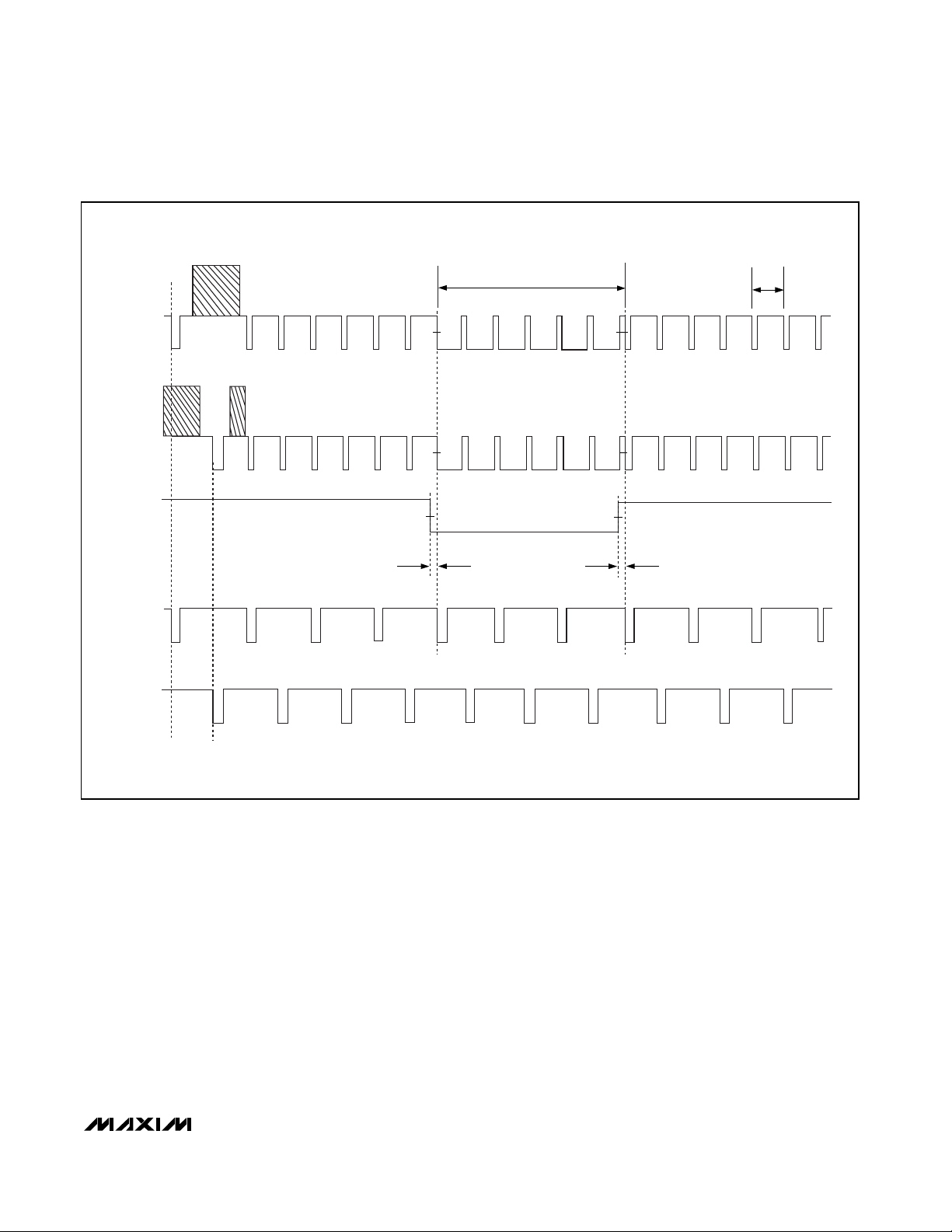
Figure 14. Detailed Serial-Interface Timing
CS
SCLK
SDIN
MSB LSB
12345678
9
10
11 121314 15 16
D7
D6
D5
D4
D3
D2
D1 D0
A6
A5
A4
A3A2A1 A0
0
Figure 15. Write Operation
CS
SCLK
SDIN
MSB
MSB
12345678
9
10
11 121314 15 16
D7
D6
D5
D4
D3
D2
D1 D0
X
A6
A5
A4
A3A2A1 A0
1
SDOUT
LSB
LSB
Figure 16. Read Operation
CS
SCLK
SDIN
MSB LSB
12345678
9
10
11 121314 15 16
00000111
L
B
C
B
L
K
I
N
V
00000
Figure 17. Writing Character Attribute Byte in 8-Bit Operation
Mode
CS
SCLK
SDIN
MSB
MSB
12345678
9
10
11 121314 15 16
L
B
C
B
L
K
I
N
V
00000
X
1011XXXX
SDOUT
LSB
LSB
Figure 18. Reading Character Attribute Byte in 8-Bit Operation
Mode

MAX7456
Resets
Power-On Reset
The MAX7456’s power-on reset circuitry (POR) provides an internal reset signal that is active after the supply voltage has stabilized. The internal reset signal
resets all registers to their default values and clears the
display memory. The register reset process requires
100µs, and to avoid unexpected results, read/write
activity is not allowed during this interval. The display
memory is reset, and the OSD is enabled typically
50ms after the supply voltage has stabilized and a stable 27MHz clock is available. The user should avoid
SPI operations during this time to avoid unexpected
results. After 50ms (typical), STAT[6] can be polled to
verify that the reset sequence is complete (Figure 22).
Single-Channel Monochrome On-Screen
Display with Integrated EEPROM
22 ______________________________________________________________________________________
CS
SCLK
SDIN
MSB LSB
12345678
9
10
11 121314 15 16
00000111
C
A
7
C
A
6
C
A
5
C
A
4
C
A
3
C
A
2
C
A
1
C
A
0
Figure 19. Writing Character Address Byte in 8-Bit and 16-Bit
Operation Modes
CS
SCLK
SDIN
MSB
12345678 12345678
9
10
11 121314 15 16
C
A
7
C
A
6
C
A
5
C
A
4
C
A
3
C
A
2
C
A
1
C
A
0
X
1011XXXX
SDOUT
LSB
MSB
L
B
C
B
L
K
I
N
V
00000
LSB
Figure 20. Reading Character Address and Character Attribute Bytes in 16-Bit Operation Mode
CS
SCLK
SDIN
MSB LSB
12345678
D7
D6
D5
D4
D3
D2
D1 D0
Figure 21. Write Operation in Auto-Increment Mode

Software Reset
The MAX7456 features a Software Reset bit (VM0[1])
that, when set high, clears the display memory and
resets all registers to their default values except the
OSD Black Level register (OSDBL). After 100µs (typical), STAT[6] can be polled to verify that the reset
process is complete.
Hardware Reset
The MAX7456 provides a hardware reset input (RESET)
that functions the same as the POR. All registers are
reset to their default values and are not accessible for
reading/writing when RESET is driven low. The resetting
process requires a ≥ 50ms wide RESET pulse, and no
other activities are allowed during this interval. All SPI
registers are reset to their default values 100µs after the
rising edge of RESET. The display memory is reset to
its default value of 00H in all locations 20µs after the rising edge of RESET. RESET takes precedence over the
Software Reset bit. After RESET has been deasserted,
STAT[6] can be polled to verify that the reset sequence
is complete.
MAX7456
Single-Channel Monochrome On-Screen
Display with Integrated EEPROM
______________________________________________________________________________________ 23
SUPPLY
VOLTAGE
XTAL
OSCILLATOR
50ms
4.75V
0V
SPI
REGISTER
RESET
100µs
50ms
DISPLAY
MEMORY
CLEAR
20µs
POWER
ON
POWER
STABLE
CLOCK
STABLE
POWER-ON
RESET START
POR DEFAULT
STAT E
Figure 22. Power-On Reset Sequence

MAX7456
MAX7456 Register Description
Access to all MAX7456 operations, including displaymemory and character-memory access, are through
the SPI registers listed in Table 3. There is no direct
access to the display and character memories through
the SPI port. See the Applications Information section
for step-by-step descriptions of the SPI operations
needed to access the memories.
The register format used in this data sheet is
REGISTER_NAME [BIT_NUMBERS]. For example, bit 1 in
Video Mode 0 register is written as VM0[1].
Single-Channel Monochrome On-Screen
Display with Integrated EEPROM
24 ______________________________________________________________________________________
Table 3. Register Map
WRITE
ADDRESS
READ
ADDRESS
REGISTER
NAME
REGISTER
DESCRIPTION
00H 80H VM0 Video Mode 0
01H 81H VM1 Video Mode 1
02H 82H HOS Horizontal Offset
03H 83H VOS Vertical Offset
04H 84H DMM Display Memory Mode
05H 85H DMAH Display Memory Address High
06H 86H DMAL Display Memory Address Low
07H 87H DMDI Display Memory Data In
08H 88H CMM Character Memory Mode
09H 89H CMAH Character Memory Address High
0AH 8AH CMAL Character Memory Address Low
0BH 8BH CMDI Character Memory Data In
0CH 8CH OSDM OSD Insertion Mux
10H 90H RB0 Row 0 Brightness
11H 91H RB1 Row 1 Brightness
12H 92H RB2 Row 2 Brightness
13H 93H RB3 Row 3 Brightness
14H 94H RB4 Row 4 Brightness
15H 95H RB5 Row 5 Brightness
16H 96H RB6 Row 6 Brightness
17H 97H RB7 Row 7 Brightness
18H 98H RB8 Row 8 Brightness
19H 99H RB9 Row 9 Brightness
1AH 9AH RB10 Row 10 Brightness
1BH 9BH RB11 Row 11 Brightness
1CH 9CH RB12 Row 12 Brightness
1DH 9DH RB13 Row 13 Brightness
1EH 9EH RB14 Row 14 Brightness
1FH 9FH RB15 Row 15 Brightness
6CH ECH OSDBL OSD Black Level
— AxH STAT Status
— BxH DMDO Display Memory Data Out
— CxH CMDO Character Memory Data Out
X = Don’t care.

Video Mode 0 Register (VM0)
Write address = 00H, read address = 80H.
Read/write access: unrestricted.
To write to this register, the following conditions must
be met:
1) STAT[5] = 0, the character memory (NVM) is not
busy.
2) DMM[2] = 0, the display memory (SRAM) is not
in the process of being cleared.
MAX7456
Single-Channel Monochrome On-Screen
Display with Integrated EEPROM
______________________________________________________________________________________ 25
BIT DEFAULT FUNCTION
7 0 Don’t Care
60
Video Standard Select
0 = NTSC
1 = PAL
5, 4 00
Sync Select Mode (Table 1)
0x = Autosync select (external sync when LOS = 0 and internal sync when LOS = 1)
10 = External
11 = Internal
30
Enable Display of OSD Image
0 = Off
1 = On
20
Vertical Synchronization of On-Screen Data
0 = Enable on-screen display immediately
1 = Enable on-screen display at the next VSYNC
10
Software Reset Bit
When this bit is set, all registers are set to their default values and the display memory is cleared.
When a stable 27MHz clock is present, this bit is automatically cleared internally after typically
100µs. The user does not need to write a 0 afterwards. SPI operations should not be performed
during this time or unpredictable results may occur. The status of the bit can be checked by
reading this register after typically 100µs. This register is not accessible for writing until the display
memory clear operation is finished (typically 20µs).
00
Video Buffer Enable
0 = Enable
1 = Disable (VOUT is high impedance)
X = Don’t care.

MAX7456
Single-Channel Monochrome On-Screen
Display with Integrated EEPROM
26 ______________________________________________________________________________________
Video Mode 1 Register (VM1)
Write address = 01H, read address = 81H.
Read/write access: unrestricted.
BIT DEFAULT FUNCTION
70
Background Mode (See Table 4)
0 = The Local Background Control bit (see DMM[5] and DMDI[7]) sets the state of each character
background.
1 = Sets all displayed background pixels to gray. The gray level is specified by bits VM1[6:4]
below. This bit overrides the local background control bit.
Note: In internal sync mode, the background mode bit is set to 1.
6, 5, 4 100
Background Mode Brightness (% of OSD White Level)
000 = 0%
001 = 7%
010 = 14%
011 = 21%
100 = 28%
101 = 35%
110 = 42%
111 = 49%
3, 2 01
Blinking Time (BT)
00 = 2 fields (33ms in NTSC mode, 40ms in PAL mode)
01 = 4 fields (67ms in NTSC mode, 80ms in PAL mode)
10 = 6 fields (100ms in NTSC mode, 120ms in PAL mode)
11 = 8 fields (133ms in NTSC mode, 160ms in PAL mode)
1, 0 11
Blinking Duty Cycle (On : Off)
00 = BT : BT
01 = BT : (2 x BT)
10 = BT : (3 x BT)
11 = (3 x BT) : BT
Horizontal Offset Register (HOS)
Write address = 02H, read address = 82H.
Read/write access: unrestricted (Figure 23).
BIT DEFAULT FUNCTION
7, 6 00 Don’t Care
5–0 10 0000
Horizontal Position Offset
(OSD video is not inserted into the horizontal blanking interval)
00 0000 = Farthest left (-32 pixels)
10 0000 = No horizontal offset
11 1111 = Farthest right (+31 pixels)

MAX7456
Single-Channel Monochrome On-Screen
Display with Integrated EEPROM
______________________________________________________________________________________ 27
Vertical Offset Register (VOS)
Write address = 03H, read address = 83H.
Read/write access: unrestricted (Figure 23).
BIT DEFAULT FUNCTION
7, 6, 5 000 Don’t Care
4–0 1 0000
Vertical Position Offset
(OSD video can be vertically shifted into the vertical blanking lines)
0 0000 = Farthest up (+16 pixels)
1 0000 = No vertical offset
1 1111 = Farthest down (-15 pixels)
Figure 23. Character Display Area
ROW NO.
0
VERTICAL POSITION OFFSET
HSYNC
DISPLAY AREA:
NTSC: 13 ROWS x 30 COLUMNS
PAL: 16 ROWS x 30 COLUMNS
HORIZONTAL POSITION OFFSET
15
VSYNC
360 PIXELS
NTSC: 234 LINES
PAL: 288 LINES

MAX7456
Single-Channel Monochrome On-Screen
Display with Integrated EEPROM
28 ______________________________________________________________________________________
Display Memory Mode Register (DMM)
Write address = 04H, read address = 84H.
Read/write access: unrestricted.
To write to this register, the following condition must be
met:
DMM[2] = 0, the display memory is not in the process
of being cleared.
BIT DEFAULT FUNCTION
7 0 Don’t Care
60
Operation Mode Selection
0 = 16-bit operation mode
The 16-bit operation mode increases the speed at which the display memory can be updated.
When writing to the display memory, the attribute byte is not entered through the SPI-compatible
interface. It is entered automatically by copying DMM[5:3] to a character’s attribute byte when a
new character is written, thus reducing the number of SPI write operations per character from two to
one (Figure 19). When in this mode, all characters written to the display memory have the same
attribute byte. This mode is useful because successive characters commonly have the same
attribute. This mode is distinct from the 8-bit operation mode where a character attribute byte must
be written each time a character address byte is written to the display memory (see Table 5). When
reading data from the display memory, both the Character Address byte and Character Attribute
byte are transferred with the SPI-compatible interface (Figure 18).
1 = 8-bit operation mode
The 8-bit operation mode provides maximum flexibility when writing characters to the display
memory. This mode enables writing individual Character Attribute bytes for each character (see
Table 5). When writing to the display memory, DMAH[1] = 0 directs the data to the Character
Address byte and DMAH[1] = 1 directs the Character Attributes byte to the data. This mode is
distinct from the 16-bit operation mode where the attribute bits are automatically copied from
DMM[5:3] when a character is written.
50
Local Background Control Bit, LBC (see Table 4)
Applies to characters written in 16-bit operating mode.
0 = Sets the background pixels of the character to the video input (VIN) when in external sync
mode.
1 = Sets the background pixels of the character to the background mode brightness level defined
by VM1[6:4] in external or internal sync mode.
Note: In internal sync mode, the local background control bit behaves as if it is set to 1.
40
Blink Bit, BLK
Applies to characters written in 16-bit operating mode.
0 = Blinking off
1 = Blinking on
Note: Blinking rate and blinking duty cycle data in the Video Mode 1 (VM1) register are used for
blinking control.
In external sync mode: when the character is not displayed, VIN is displayed.
In internal sync mode: when the character is not displayed, background mode brightness is
displayed (see VM1[6:4]).
30
Invert Bit, INV
Applies to characters written in 16-bit operating mode (see Figure 24).
0 = Normal (white pixels display white, black pixels display black)
1 = Invert (white pixels display black, black pixels display white)

MAX7456
Single-Channel Monochrome On-Screen
Display with Integrated EEPROM
______________________________________________________________________________________ 29
Display Memory Mode Register (DMM) (continued)
BIT DEFAULT FUNCTION
20
Clear Display Memory
0 = Inactive
1 = Clear (fill all display memories with zeros)
Note: This bit is automatically cleared after the operation is completed (the operation requires
20µs). The user does not need to write a 0 afterwards. The status of the bit can be checked by
reading this register.
This operation is automatically performed:
a) On power-up
b) Immediately following the rising edge of RESET
c) Immediately following the rising edge of CS after VM0[1] has been set to 1
10
Vertical Sync Clear
Valid only when clear display memory = 1, (DMM[2] = 1)
0 = Immediately applies the clear display-memory command, DMM[2] = 1
1 = Applies the clear display-memory command, DMM[2] = 1, at the next VSYNC time
00
Auto-Increment Mode
Auto-increment mode increases the speed at which the display memory can be written by
automatically incrementing the character address for each successive character written. This mode
reduces the number of SPI commands, and thus the time needed to write a string of adjacent
characters. This mode is useful when writing strings of characters written from left-to-right, top-tobottom, on the display (see Table 5).
0 = Disabled
1 = Enabled
When this bit is enabled for the first time, data in the Display Memory Address (DMAH[0] and
DMAL[7:0]) registers are used as the starting location to which the data is written. When performing
the auto-increment write for the display memory, the 8-bit address is internally generated, and
therefore only 8-bit data is required by the SPI-compatible interface (Figure 21). The content is to
be interpreted as a Character Address byte if DMAH[1] = 0 or a Character Attribute byte if
DMAH[1] = 1. This mode is disabled by writing the escape character 1111 1111.
If the Clear Display Memory bit is set, this bit is reset internally.

MAX7456
Single-Channel Monochrome On-Screen
Display with Integrated EEPROM
30 ______________________________________________________________________________________
INVERT
BIT
DMM[3]
EXTERNAL SYNC MODE AND LOCAL
BACKGROUND CONTROL BIT (LBC) = 0
INTERNAL SYNC MODE OR LOCAL
BACKGROUND CONTROL BIT (LBC) = 1
0
1
Figure 24. Character Attribute Bit Examples: Invert and Local Background Control

MAX7456
Single-Channel Monochrome On-Screen
Display with Integrated EEPROM
______________________________________________________________________________________ 31
Table 4. Character Background Control
SYNC MODE
BACKGROUND MODE,
VM1[7]
LOCAL BACKGROUND
CONTROL BIT, LBC
DMM[5], DMDI[7]
CHARACTER
BACKGROUND PIXEL
0 0 Input Video
0 1 Gray
External
1 X Gray
Internal X X Gray
X = Don’t care.
Display Memory Address High Register
(DMAH)
Write address = 05H, read address = 85H.
Read/write access: unrestricted.
To write to this register, the following condition must be
met:
DMM[2] = 0, the display memory is not in the process
of being cleared.
BIT DEFAULT FUNCTION
7–2 0000 00 Don’t Care
10
Byte Selection Bit
This bit is valid only when in the 8-bit operation mode (DMM[6] = 1).
0 = Character Address byte is written to or read (DMDI[7:0] contains the Character Address byte).
1 = Character Attribute byte is written to or read (DMDI[7:0] contains the Character Attribute byte).
00
Display Memory Address Bit 8
This bit is the MSB of the display-memory address. The display-memory address sets the location
of a character on the display (Figure 10). The lower order 8 bits of the display-memory address is
found in DMAL[7:0].
Display Memory Address Low Register
(DMAL)
Write address = 06H, read address = 86H.
Read/write access: unrestricted.
To write to this register, the following condition must be
met:
DMM[2] = 0, the display memory is not in the process
of being cleared.
BIT DEFAULT FUNCTION
7–0 0000 0000
Display Memory Address Bits 7–0
This byte is the lower 8 bits of the display-memory address. The display-memory address sets the
location of a character on the display (Figure 10). The MSB of the display-memory address is
DMAH[0].

MAX7456
Single-Channel Monochrome On-Screen
Display with Integrated EEPROM
32 ______________________________________________________________________________________
Display Memory Data In Register (DMDI)
Write address = 07H, read address = 87H.
Read/write access: unrestricted.
To write to this register, the following condition must be
met:
DMM[2] = 0, the display memory is not in the process
of being cleared.
BIT DEFAULT FUNCTION
7–0 0000 0000
Character Address or Character Attribute byte to be stored in the display memory.
8-Bit Operation Mode (DMM[6] = 1)
If DMAH[1] = 0, the content is to be interpreted as a Character Address byte, where
Bits 7–0 = Character Address bits, CA[7:0] (Figure 12).
If DMAH[1] = 1, the content is to be interpreted as a Character Attribute byte where
Bit 7 = Local Background Control bit, LBC (Figure 24 and Table 4)
Bit 6 = Blink bit, BLK
Bit 5 = Invert bit, INV (see Figure 24)
Bit 4–0 = 0
(The LBC, BLK, and INV bits are described in the Display Memory Mode register.)
16-Bit Operation Mode (DMM[6] = 0)
The content is always interpreted as a Character Address byte where bits 7–0 =
CA[7:0] (Figure 12).
Auto-Increment Mode (DMM[0] = 1)
The character address CA[7:0] = FFH is reserved for use as an escape character that terminates
the auto-increment mode. Therefore, the character located at address FFH is not available for
writing to the display memory when in auto-increment mode. In all other modes, character FFH is
available.

MAX7456
Single-Channel Monochrome On-Screen
Display with Integrated EEPROM
______________________________________________________________________________________ 33
Character Memory Mode Register (CMM)
Write address = 08H, read address = 88H.
Read/write access: unrestricted.
To write to this register, the following conditions must
be met:
1) STAT[5] = 0, the character memory (NVM) is not
busy.
2) VM0[3] = 0, the OSD is disabled.
X = Don’t care.
BIT DEFAULT FUNCTION
7–0 0000 0000
Only whole characters (54 bytes) can be written to or read from the nonvolatile character memory
(NVM) at one time. This is done through the (64 byte) shadow RAM (Figure 13). The shadow RAM is
accessed through the SPI port one byte at a time. The shadow RAM is written to and read from
NVM by the following procedures:
Writing to NVM
1010 XXXX = Write to NVM array from shadow RAM.
The 64 bytes from shadow RAM are written to the NVM array at the character-memory address
location (CMAH, CMAL) (Figure 13). The character memory is busy for approximately 12ms during
this operation. During this time, STAT[5] is automatically set to 1. The Character Memory Mode
register is cleared and STAT[5] is reset to 0 after the write operation has been completed. The user
does not need to write zeros afterwards.
Reading from NVM
0101 XXXX = Read from NVM array into shadow RAM.
The 64 bytes corresponding to the character-memory address (CMAH, CMAL) are read from the
NVM array into the shadow RAM (Figure 13). The character memory is busy for approximately 0.5µs
during this operation. The CMM register is cleared after the operation is completed. The user does
not need to write zeros afterwards. During this time, STAT[5] is automatically set to 1. STAT[5] is
reset to 0 when the read operation has been complete.
If the display has been enabled (VM0[3] = 1) or the character memory is busy (STAT[5] = 1), NVM
read/write operation commands are ignored and the corresponding registers are not updated.
However, all the registers can be read at any time.
For all the character-memory operations, the character address is formed with Character Memory
Address High (CMAH[7:0]) and Character Memory Address Low (CMAL[7:0]) register bits (Figures
11, 12, and 13).

MAX7456
Single-Channel Monochrome On-Screen
Display with Integrated EEPROM
34 ______________________________________________________________________________________
Character Memory Address High Register
(CMAH)
Write address = 09H, read address = 89H.
Read/write access: unrestricted.
To write to this register, the following conditions must
be met:
1) STAT[5] = 0, the character memory (NVM) is not
busy.
2) VM0[3] = 0, the OSD is disabled.
BIT DEFAULT FUNCTION
7–0 0000 0000
Character Memory Address Bits
These 8 bits point to a character in the character memory (256 characters total in NVM) (Figures 10
and 12).
Character Memory Address Low Register
(CMAL)
Write address = 0AH, read address = 8AH.
Read/write access: unrestricted.
To write to this register, the following conditions must
be met:
1) STAT[5] = 0, the character memory (NVM) is not
busy.
2) VM0[3] = 0, the OSD is disabled.
BIT DEFAULT FUNCTION
7, 6 00 Don’t Care
5–0 00 0000
Character Memory Address Bits
These 6 bits point to one of the 64 bytes (only 54 used) that represent a 4-pixel group in the
character (Figures 10 and 11).
Character Memory Data In Register (CMDI)
Write address = 0BH, read address = 8BH.
Read/write access: unrestricted.
To write to this register, the following conditions must
be met:
1) STAT[5] = 0, the character memory (NVM) is not
busy.
2) VM0[3] = 0, the OSD is disabled.
BIT DEFAULT FUNCTION
7, 6 NA Leftmost pixel. 00 = Black, 10 = White, 01 or 11 = Transparent (see Figure 11)
5, 4 NA Left center pixel. 00 = Black, 10 = White, 01 or 11 = Transparent (see Figure 11)
3, 2 NA Right center pixel. 00 = Black, 10 = White, 01 or 11 = Transparent (see Figure 11)
1, 0 NA Rightmost pixel. 00 = Black, 10 = White, 01 or 11 = Transparent (see Figure 11)
NA = Not applicable.

MAX7456
Single-Channel Monochrome On-Screen
Display with Integrated EEPROM
______________________________________________________________________________________ 35
OSD Insertion Mux Register (OSDM)
Write address = 0CH, read address = 8CH.
Read/write access: unrestricted.
BIT DEFAULT FUNCTION
7, 6 00 Don’t Care
5, 4, 3 011
OSD Rise and Fall Time—typical transition times between adjacent OSD pixels
000: 20ns (maximum sharpness/maximum crosscolor artifacts )
001: 30ns
010: 35ns
011: 60ns
100: 80ns
101: 110ns (minimum sharpness/minimum crosscolor artifacts)
2, 1, 0 011
OSD Insertion Mux Switching Time–typical transition times between input video and OSD pixels
000: 30ns (maximum sharpness/maximum crosscolor artifacts )
001: 35ns
010: 50ns
011: 75ns
100: 100ns
101: 120ns (minimum sharpness/minimum crosscolor artifacts)
Row N Brightness Register
(RB0–RB15)
Address = 10H + row number; write address = 10H
through 1FH, read address = 90H through 9FH,
read/write access: unrestricted.
Top row number is 0. Bottom row number is 13 in NTSC
mode and 15 in PAL mode (see Figure 23).
BIT DEFAULT FUNCTION
7–4 0000 Don’t Care
3, 2 00
Character Black Level —All the characters in row N use these brightness levels for the black pixel,
in % of OSD white level.
00 = 0%
01 = 10%
10 = 20%
11 = 30%
1, 0 01
Character White Level —All the characters in row N use these brightness levels for the white pixel,
in % of OSD white level.
00 = 120%
01 = 100%
10 = 90%
11 = 80%

MAX7456
Single-Channel Monochrome On-Screen
Display with Integrated EEPROM
36 ______________________________________________________________________________________
OSD Black Level Register (OSDBL)
Write address = 6CH, read address = ECH.
Read/write access: This register contains 4 factory-preset bits [3:0] that must not be changed. Therefore,
when changing bit 4, first read this register, modify bit
4, and then write back the updated byte.
BIT DEFAULT FUNCTION
7–5 000 Don’t Care
41
OSD Image Black Level Control
This bit enables the alignment of the OSD image black level with the input image black level at
VOUT. Always enable this bit following power-on reset to ensure the correct OSD image brightness.
0 = Enable automatic OSD black level control
1 = Disable automatic OSD black level control
0–3 xxxx
These bits are factory preset. To ensure proper operation of the MAX7456, do not change the
values of these bits.
xxxx = Factory preset—can be any one of the 16 possible values. This value is permanently stored in the MAX7456 and will always
be restored to the factory preset value following power-on reset or hardware reset.
Status Register (STAT)
Read address = AxH.
Read/write access: read only.
BIT DEFAULT FUNCTION
7 NA Don’t Care
6NA
Reset M od e
0 = C l ear w hen p ow er - up r eset m od e i s com p l ete. O ccur s 50m s ( typ ) fol l ow i ng stab l e V
D D
( Fi g ur e 22)
1 = S et w hen i n p ow er - up r eset m od e
5NA
Character Memory Status
0 = Available to be written to or read from
1 = Unavailable to be written to or read from
4NA
VSYNC Output Level
0 = Active during vertical sync time
1 = Inactive otherwise
3NA
HSYNC Output Level
0 = Active during horizontal sync time
1 = Inactive otherwise
2NA
Loss-of-Sync (LOS)
0 = Sync Active. Asserted after 32 consecutive input video lines.
1 = No Sync. Asserted after 32 consecutive missing input video lines.
1NA
0 = NTSC signal is not detected at VIN
1 = NTSC signal is detected at VIN
0NA
0 = PAL signal is not detected at VIN
1 = PAL signal is detected at VIN
NA = Not applicable.
X = Don’t care.

MAX7456
Single-Channel Monochrome On-Screen
Display with Integrated EEPROM
______________________________________________________________________________________ 37
Display Memory Data Out Register (DMDO)
Read address = BxH.
Read/write access: read only.
To write to this register the following condition must be
met:
DMM[2] = 0, the display memory is not in the process
of being cleared.
BIT DEFAULT FUNCTION
7–0 NA
Character Address or Character Attribute byte to be read from the display memory.
8-Bit Operation Mode (DMM[6] = 1):
If DMAH[1] = 0, the content is to be interpreted as a Character Address byte, where
Bits 7–0 = Character Address bits, CA[7:0] (Figure 12)
If DMAH[1] = 1, the content is to be interpreted as a Character Attribute byte where
Bit 7 = Local Background Control bit, LBC (see Figure 24 and Table 4)
Bit 6 = Blink bit, BLK
Bit 5 = Invert bit, INV (see Figure 24)
Bit 4–0 = 0
The LBC, BLK, and INV bits are described in the Display Memory Mode register.
16-Bit Operation Mode (DMM[6] = 0):
The content is to be interpreted as a Character Address byte, where
Bits 7–0 = CA[7:0] (see Figure 12)
followed by a Character Attribute byte, where
Bit 7 = 0
Bit 6 = Local Background Control bit, LBC (see Figure 24 and Table 4)
Bit 5 = Blink bit, BLK
Bit 4 = Invert bit, INV (see Figure 24)
Bit 3–0 = 0
The LBC, BLK, and INV bits are described in the Display Memory Mode register.
NA = Not applicable.
X = Don’t care.
Character Memory Data Out Register
(CMDO)
Read address = CxH.
Read/write access: read only.
To write to this register, the following conditions must
be met:
1) STAT[5] = 0, the character memory (NVM) is not
busy.
2) VM0[3] = 0, the OSD is disabled.
BIT DEFAULT FUNCTION
7, 6 NA Leftmost pixel. 00 = Black, 10 = White, 01 or 11 = Transparent (see Figure 11)
5, 4 NA Left center pixel. 00 = Black, 10 = White, 01 or 11 = Transparent (see Figure 11)
3, 2 NA Right center pixel. 00 = Black, 10 = White, 01 or 11 = Transparent (see Figure 11)
1, 0 NA Rightmost pixel. 00 = Black, 10 = White, 01 or 11 = Transparent (see Figure 11)
NA = Not applicable.
X = Don’t care.

MAX7456
Single-Channel Monochrome On-Screen
Display with Integrated EEPROM
38 ______________________________________________________________________________________
Applications Information
Character-Memory Operation
Only whole characters (54 bytes of pixel data) can be
written to or read from the NVM character memory at one
time. This is done through the (64 byte) shadow RAM
(see Figure 13). The shadow RAM is accessed by the
SPI port one byte at a time. The shadow RAM is written
to and read from the NVM by a single SPI command.
Steps for Writing Character Bytes
into the NVM Character Memory
Writing a new character:
1) Write VM0[3] = 0 to disable the OSD image display.
2) Write CMAH[7:0] = xxH to select the character
(0–255) to be written (Figures 10 and 13).
3) Write CMAL[7:0] = xxH to select the 4-pixel byte
(0–63) in the character to be written (Figures 10 and
13).
4) Write CMDI[7:0] = xxH to set the pixel values of the
selected part of the character (Figures 11 and 13).
5) Repeat steps 3 and 4 until all 54 bytes of the character data are loaded into the shadow RAM.
6) Write CMM[7:0] = 1010xxxx to write to the NVM
array from the shadow RAM (Figure 13). The character memory is busy for approximately 12ms during this operation. STAT[5] can be read to verify that
the NVM writing process is complete.
7) Write VM0[3] = 1 to enable the OSD image display.
Modifying an existing character:
1) Write VM0[3] = 0 to disable the OSD image display.
2) Write CMAH[7:0] = xxH to select the character
(0–255) to be modified (Figures 10 and 13).
3) Write CMM[7:0] = 0101xxxx to read character data
from the NVM to the shadow RAM (Figure 13).
4) Write CMAL[7:0] = xxH to select the 4-pixel byte
(0–63) in the character to be modified (Figures 10
and 13).
5) Read CMDO[7:0] = xxH to read the byte of 4-pixel
data to be modified (Figures 11 and 13).
6) Modify the byte of 4-pixel data as desired.
7) Write CMDI[7:0] = xxH to write the modified byte of
4-pixel data back to the shadow RAM (Figures 11
and 13).
8) Repeat steps 4 through 7 as needed until all pixels
have been loaded into the shadow RAM.
9) Write CMM[7:0] = 1010xxxx to write the shadow
RAM data to the NVM (Figure 13). The character
memory is busy for typically 12ms during this operation. STAT[5] can be read to verify that the NVM
writing process is complete.
10) Write VM0[3] =1 to enable the OSD image display.
Steps for Reading Character
Bytes from Character Memory
1) Write VM0[3] = 0 to disable the OSD image.
2) Write CMAH[7:0] = xxH to select the character
(0–255) to be read (Figures 10 and 13).
3) Write CMM[7:0] = 0101xxxx to read the character
data from the NVM to the shadow RAM (Figure 13).
4) Write CMAL[7:0] = xxH to select the 4-pixel byte
(0–63) in the character to be read (Figures 10 and 13).
5) Read CMDO[7:0] = xxH to read the selected 4-pixel
byte of data (Figures 11 and 13).
6) Repeat steps 4 and 5 to read other bytes of 4-pixel
data.
7) Write VM0[3] = 1 to enable the OSD image display.
Display-Memory Operation
The following two steps enable viewing of the OSD
image. These steps are not required to read from or
write to the display memory:
1) Write VM0[3] = 1 to enable the display of the OSD
image.
2) Write OSDBL[4] = 0 to enable automatic OSD black
level control. This ensures the correct OSD image
brightness. This register contains 4 factory-preset
bits [3:0] that must not be changed. Therefore,
when changing bit 4, first read OSDBL[7:0], modify
bit 4, and then write back the updated byte.
Steps for Clearing Display Memory
Write DMM[2] = 1 to start the clear display-memory
operation. This operation typically takes 20µs. The
Display Memory Mode register cannot be written to
again until the clear operation is complete. DMM[2] is
automatically reset to zero upon completion.
Steps for Writing to
Display Memory in 8-Bit Mode
The 8-bit operation mode provides maximum flexibility
when writing characters to the display memory. This
mode enables writing individual Character Attribute
bytes for each character (see Table 5). This mode is
distinct from the 16-bit operation mode where the
Character Attribute byte is automatically copied from
DMM[5:3] when a character is written (Figure 19).
Write DMM[6] = 1 to select the 8-bit operation mode.

Writing the Character Address Byte to the Display
Memory:
1) Write DMAH[1] = 0 to write a Character Address
byte.
2) Write DMAH[0] = x to select the MSB and
DMAL[7:0] = xxH to select the lower order bits of
the address where the character data is to be written. This address determines the location of the
character on the display (see Figure 10).
3) Write the Character Address byte (CA[7:0]) to be
written to the display memory to DMDI[7:0] (see
Figures 10, 12, and 19).
Writing the Character Attribute Byte to the Display
Memory:
1) Write DMAH[1] = 1 to write a Character Attribute
byte.
2) Write DMAH[0] = x to select the MSB and
DMAL[7:0] = xxH to select the lower order bits of
the address where the character data is to be written. This address determines the location of the
character on the display (Figure 10).
3) Write the Character Attribute byte to be written to
the display memory to DMDI[7:0] (see Figures 10
and 19).
Steps for Writing to
Display Memory in 16-Bit Mode
The 16-bit operation mode increases the speed at
which the display memory can be updated. This is
done by automatically copying DMM[5:3] to a
Character’s Attribute byte when a new character is written, thus reducing the number of SPI write operations
per character from two to one (Figure 19). When in this
mode, all characters written to the display memory
have the same attribute byte. This mode is useful
because successive characters commonly have the
same attribute. This mode is distinct from the 8-bit
operation mode where a Character Attribute byte must
be written each time a Character Address byte is written to the display memory (see Table 5).
1) Write DMM[6] = 0 to select the 16-bit operation
mode.
2) Write DMM[5:3] = xxx to set the Local Background
Control (LBC), Blink (BLK), and Invert (INV) attribute
bits that will be applied to all characters written to
the display memory while in the 16-bit operation
mode.
3) Write DMAH[0] = x to select the MSB and
DMAL[7:0] = xxH to select the lower order bits of the
address where the character data is to be written.
This address determines the location of the character on the display (see Figure 10).
4) Write the Character Address byte (CA[7:0]) to be
written to the display memory into DMDI[7:0]. It will
be stored along with a Character Attribute byte
derived from DMM[5:3] (Figures 12 and 19).
Steps for Writing to Display Memory
in Auto-Increment Mode
Auto-increment mode increases the speed at which the
display memory can be written by automatically incrementing the character address for each successive
character written. This mode is useful when writing
strings of characters written from left-to-right and topto-bottom on the display. This mode reduces the number of SPI commands (see Table 5).
When in 8-Bit Operating Mode:
1) Write DMM[0] = 1 to set the auto-increment mode.
2) Write to DMM[6] = 1 to set the 8-bit operation mode.
3) Write DMAH[1] = 0 to select if a Character Address
byte will be written or DMAH[1] = 1 to select if a
Character Attribute byte will be written.
4) Write DMAH[0] = x to select the MSB and
DMAL[7:0] to select the lower order address bits, of
the starting address for auto-increment operation.
This address determines the location of the character on the display (see Figures 10 and 21).
5) Write to DMDI[7:0] to store character data (Character
Address or Character Attribute bytes) to the current
display-memory address. The display-memory
address is automatically incremented following the
write operation. Subsequent characters are successively written from left-to-right and top-to-bottom on the
display (see Figure 10). Repeat until the final displaymemory address is reached.
6) Write DMDI[7:0] = FFH to terminate the auto-increment mode. Note that the character stored at
CA[7:0] = FFH is not available for use when in autoincrement mode.
When in 16-Bit Operating Mode:
1) Write DMM[0] = 1 to set the auto-increment mode.
2) Write DMM[6] = 0 to set the 16-bit operation mode.
3) Write DMM[5:3] = xxx to set the Local Background
Control (LBC), Blink (BLK), and Invert (INV) attribute
bits that will be applied to all characters.
4) Write DMAH[0] = x to select the MSB and
DMAL[7:0] to select the lower order address bits, of
the starting address for auto-increment operation.
MAX7456
Single-Channel Monochrome On-Screen
Display with Integrated EEPROM
______________________________________________________________________________________ 39

MAX7456
This address determines the location of the character on the display (see Figures 10 and 21).
5) Write the Character Address byte (CA[7:0]) to be
written to the display memory into DMDI[7:0]. It will
be stored along with a Character Attribute byte
derived from DMM[5:3] (see Figure 19). The display-memory address is automatically incremented
following the write operation. Repeat until the final
display-memory address is reached.
6) Write DMDI[7:0] = FFH to terminate the auto-increment mode. Note that the character stored at
CA[7:0] = FFH is not available for use when in autoincrement mode.
Steps for Reading from Display
Memory in 8-Bit Mode
1) Write DMM[6] = 1 to select the 8-bit operation mode.
2) Write DMAH[1] = 0 to read the Character Address
byte or DMAH[1] = 1 to read the Character Attribute
byte.
3) Write to DMAH[0] to select the MSB of the address
where data must be read from (Figure 10).
4) Write to DMAL[7:0] to select all the lower order bits,
except for the MSB, of the address where data must
be read from (Figure 10).
5) Read DMDO[7:0] to read the data from the selected
location in the display memory (Figure 10).
Steps for Reading from Display
Memory in 16-Bit Mode
1) Write DMM[6] = 0 to select the 16-bit operation
mode.
2) Write DMAH[0] = x to select the MSB and
DMAL[7:0] = xxH to select the lower order bits of
the address where the character data is to be read.
This address determines the location of the character on the display (see Figure 10).
3) Read DMDO[15:0] to read the Character Address
byte and the Character Attribute byte from the
selected location in the display memory. The first
data byte is the Character Address (CA[7:0]), and
the second byte contains the Character Attribute
bits (Figure 20). Note that the bit positions of the
Character Attribute byte when read, differ from
when they are written. See the Display Memory Data
Out Register (DMDO) section and Figure 20 for a
description of the bit locations of the attribute bits
when reading.
Note: If an internal display-memory read request
occurs simultaneously with an SPI display-memory
operation, the internal read request is ignored, and the
display of that character, during that field time, may
appear to momentarily break up. See the Synchronous
OSD Updates section.
Synchronous OSD Updates
The display of a character may momentarily appear to
break up if an internal display-memory read request
occurs simultaneously with an SPI display-memory
operation. Momentary breakup of the OSD image can
be prevented by writing to the display memory during
the vertical blanking interval. This can be achieved by
using VSYNC as an interrupt to the host processor to
initiate writing to the display memory. Alternatively, the
OSD image can be synchronously disabled before writing to the display memory and synchronously reenabled afterwards (see VM0[3:2]).
Multiple OSDs with
Common Clock Application
The MAX7456 provides a TTL clock output (CLKOUT)
capable of driving one CLKIN pin of another MAX7456.
Two or more MAX7456 parts can be driven using an
external clock driver. This arrangement reduces the
system cost by having only one crystal on one
MAX7456 that supplies the clock signal to multiple
MAX7456 parts (Figure 25).
Single-Channel Monochrome On-Screen
Display with Integrated EEPROM
40 ______________________________________________________________________________________
Table 5. Display-Memory Access Modes and SPI Operations
OPERATING
MODE
AUTO-INCREMENT
DMM[0] = 0
No. OF READ
OPERATIONS
No. OF WRITE
OPERATIONS
AUTO-INCREMENT
DMM[0] = 1
No. OF WRITE
OPERATIONS
One-time setup 2 1 One-time setup 6
16-Bit Mode
DMM[6] = 0
Per character 3 3 Per character 1
One-time setup 1 1 One-time setup 6
8-Bit Mode
DMM[6] = 1
Per character 6 6 Per character 1
MODE DISABLED
MODE ENABLED

MAX7456
Single-Channel Monochrome On-Screen
Display with Integrated EEPROM
______________________________________________________________________________________ 41
28
27
26
25
24
23
22
21
20
19
18
17
16
15
1
2
3
4
5
6
7
8
9
10
11
12
13
14
MAX7456
SDIN
+5V
27MHz
SDOUT
+5V
CVBS OUT1
SAG
PGND
RESET
HSYNC
VSYNC
DGND
CLKIN
XFB
CLKOUT
CS
SDIN
SCLK
SDOUT
LOS
N.C.
SCLK
CS1
CVBS IN1
LOS1
VS1
HS1
N.C.
N.C.
N.C.
N.C.
N.C.
AGND
N.C.
N.C.
+5V
0.1µF
C
OUT
75Ω
75Ω
1kΩ1kΩ1kΩ
0.1µF
+5V
1kΩ1kΩ1kΩ
0.1µF
0.1µF
C
SAG
C
OUT
C
SAG
28
27
26
25
24
23
22
21
20
19
18
17
16
15
1
2
3
4
5
6
7
8
9
10
11
12
13
14
MAX7456
+5V
CLOCK
DRIVER
+5V
CVBS OUT2
SAG
PGND
RESET
HSYNC
VSYNC
DVDD
DGND
CLKIN
XFB
CLKOUT
CS
SDIN
SCLK
SDOUT
LOS
N.C.
CS2
CVBS IN2
LOS2
VS2
HS2
N.C.
N.C.
N.C.
N.C.
N.C.
AGND
N.C.
N.C.
0.1µF
TO OTHER
MAX7456 PARTS
AS NEEDED
VOUT
PVDD
VIN
AVDD
75Ω
75Ω
0.1µF
0.1µF
0.1µF
DVDD
VOUT
PVDD
VIN
AVDD
+
+
Figure 25. Typical Multiple OSDs with Daisy-Chained Clock

MAX7456
Single-Channel Monochrome On-Screen
Display with Integrated EEPROM
42 ______________________________________________________________________________________
Selecting a Clock Crystal
Choose a 27MHz parallel resonant, fundamental mode
crystal. No external load capacitors are needed. All
capacitors required for the Pierce oscillator are included on-chip.
Power Supply and Bypassing
The MAX7456 operates from three independent supply
lines. Each supply must be within a +4.75V to +5.25V
voltage range. Separate the digital power supply from
the analog and video-driver supply lines to prevent
high-frequency digital noise that may couple onto the
video output. All three supplies should be at the same
DC voltage. Bypass each supply with a 0.1µF capacitor
to ground very close to the IC pins. There are no
power-supply sequencing requirements for the device.
Layout Concerns
For best performance, make the VIN and VOUT traces
as short as possible. Place all AC-coupling capacitors
and 75Ω termination resistors close to the device with
the resistors terminated to the solid analog ground
plane. Since the MAX7456 TSSOP package has an
exposed pad (EP) underneath, do not run traces under
the package to avoid possible short circuits. Refer to
the MAX7456 EV kit for an example of PCB layout.
To aid heat dissipation, the EP should be connected to
a similarly sized pad on the component side of the
PCB. This pad should be connected through to the solder-side copper by several plated holes to conduct
heat away from the device. The solder-side copper pad
area should be larger than the EP area. It is recommended that the EP be connected to ground, but it is
not required. Do not use EP as the only ground connection for the device.
28
27
26
25
24
23
22
21
20
19
18
17
16
15
1
2
3
4
5
6
7
8
9
10
11
12
13
14
N.C.
N.C.
VOUT
SAG
PVDD
PGND
N.C.
VIN
AVDD
AGND
RESET
HSYNC
VSYNC
N.C.
N.C.
N.C.
LOS
SDOUT
SCLK
SDIN
CS
CLKOUT
XFB
CLKIN
DGND
DVDD
N.C.
N.C.
TSSOP
TOP VIEW
MAX7456
+
Pin Configuration
Chip Information
PROCESS: BiCMOS

MAX7456
Single-Channel Monochrome On-Screen
Display with Integrated EEPROM
Maxim cannot assume responsibility for use of any circuitry other than circuitry entirely embodied in a Maxim product. No circuit patent licenses are
implied. Maxim reserves the right to change the circuitry and specifications without notice at any time.
Maxim Integrated Products, 120 San Gabriel Drive, Sunnyvale, CA 94086 408-737-7600 ____________________ 43
© 2007 Maxim Integrated Products is a registered trademark of Maxim Integrated Products, Inc.
Package Information
(The package drawing(s) in this data sheet may not reflect the most current specifications. For the latest package outline information,
go to www.maxim-ic.com/packages
.)
AA AA
TSSOP 4.4mm BODY.EPS
 Loading...