MAXIM MAX7446 Technical data

现货库存、技术资料、百科信息、热点资讯,精彩尽在鼎好!
General Description
The MAX7446 4-channel, buffered video reconstruction
filter is ideal for anti-aliasing and DAC-smoothing video
applications or wherever analog video is reconstructed
from a digital data stream (such as cable/satellite/terrestrial set-top boxes, DVD players, hard disk recorders
(HDRs), and personal video recorders (PVRs)). This
device operates from a single +5V supply and has a
flat passband out to 5MHz with a stopband attenuation
of 43dB at 27MHz. This makes it ideal for use with
NTSC, PAL, and standard-definition digital TV (SDTV)
video systems. Each output is capable of driving two
standard 150Ω video loads.
The MAX7446 processes CVBS and RGB video signals.
The video output buffers have a fixed gain of +6dB. The
channel for CVBS video has high-frequency boost circuitry
that provides picture sharpness with +1.2dB of gain
boost without degradation in the stopband. The output
video drivers can be disabled with an external pin.
The MAX7446 is available in a 14-pin TSSOP package
with an exposed pad, and is specified over the -40°C to
+85°C extended temperature range.
Applications
Set-Top Boxes/HDRs Game Consoles
Desktop Video Editors DVD Players
Digital VCRs
Features
♦ 4-Channel Filter and Buffer for RGB and
CVBS Signals
♦ Filter Response Ideal for NTSC, PAL, and
Interlaced SDTV Video Signals
♦ 43dB (typ) Stopband Attenuation at 27MHz
♦ ±0.75dB (max) Passband Ripple Out to 5MHz
♦ Blanking Level Voltage on Cable <1V
♦ Each Channel Drives Two 150Ω Video Loads
♦ +5V Single-Supply Voltage
♦ Small 14-Pin TSSOP Package
MAX7446
4-Channel Video Filter for RGB and CVBS Video
________________________________________________________________ Maxim Integrated Products 1
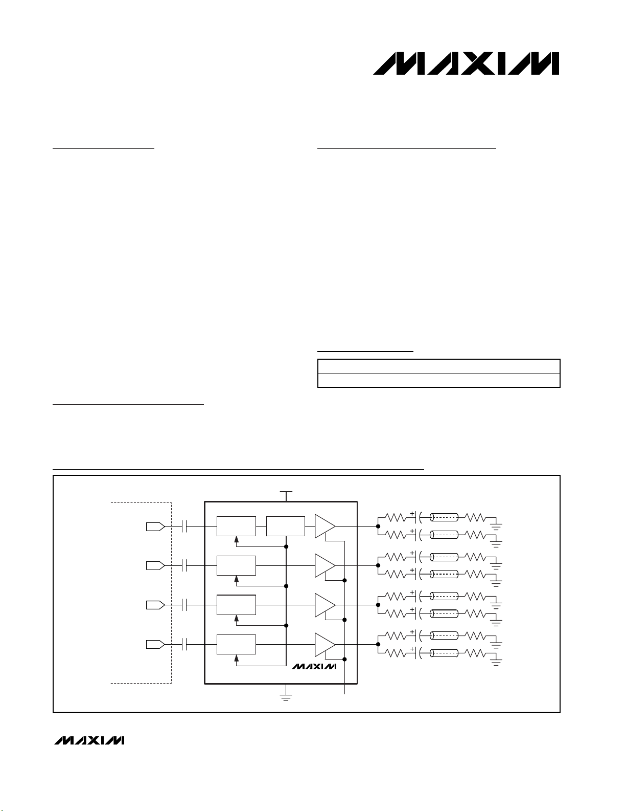
Functional Diagram
Ordering Information
19-2951; Rev 0; 8/03
For pricing, delivery, and ordering information, please contact Maxim/Dallas Direct! at
1-888-629-4642, or visit Maxim’s website at www.maxim-ic.com.
*EP = Exposed pad.
Pin Configuration appears at end of data sheet.
PART TEMP RANGE PIN-PACKAGE
MAX7446EUD -40°C to +85°C 14 TSSOP-EP*
*
*
*
*
*
*
*
*
75Ω
75Ω
75Ω
75Ω
75Ω
75Ω
75Ω
75Ω
ENCODER
CVBS
(WITHOUT SYNC)
V
CC
0.1µF
0.1µF
0.1µF
0.1µF
INA
INB
INC
IND
D/A
R
D/A
G
D/A
B
D/A
LOWPASS
FILTER
LOWPASS
FILTER
LOWPASS
FILTER
LOWPASS
FILTER
SYNC
DETECTOR
GND
MAX7446
DISABLE
75Ω
OUTA
75Ω
75Ω
OUTB
75Ω
75Ω
OUTC
75Ω
75Ω
OUTD
75Ω
*OPTIONAL CAPACITORS

MAX7446
4-Channel Video Filter for RGB and CVBS Video
2 _______________________________________________________________________________________
ABSOLUTE MAXIMUM RATINGS
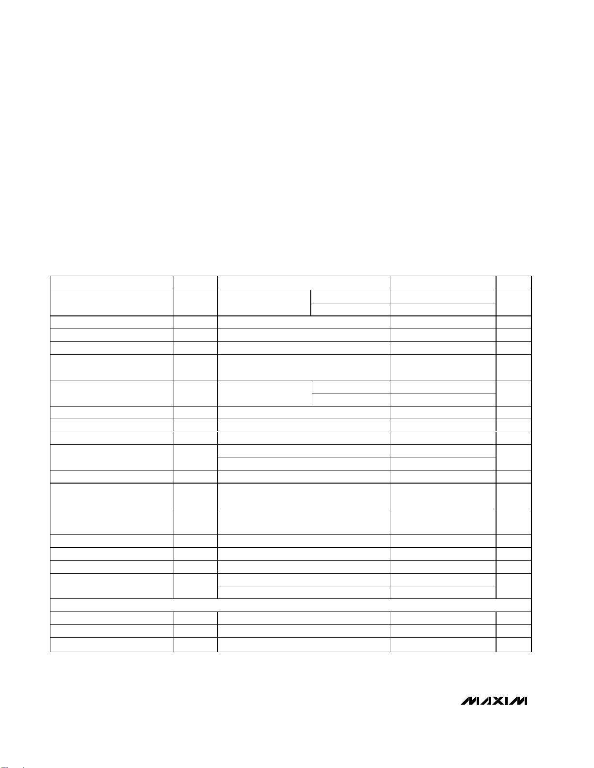
ELECTRICAL CHARACTERISTICS
(V
CC
= +5V ±5%, CL= 0 to 20pF, RL= 75Ω to GND for DC-coupled load, RL= 75Ω to V
CC
/ 2 for AC-coupled load, C
IN_
= 0.1µF,
T
A
= T
MIN
to T
MAX
, unless otherwise noted. Typical values are at VCC= +5V, TA= +25°C.)
Stresses beyond those listed under “Absolute Maximum Ratings” may cause permanent damage to the device. These are stress ratings only, and functional
operation of the device at these or any other conditions beyond those indicated in the operational sections of the specifications is not implied. Exposure to
absolute maximum rating conditions for extended periods may affect device reliability.
VCCto GND ...........................................................................+6V
All Other Pins to GND.................................-0.3V to (V
CC
+ 0.3V)
Maximum Current into Any Pin Except V
CC
and GND .....±50mA
Continuous Power Dissipation (T
A
= +70°C)
TSSOP-EP (derate 20.8mW/°C above +70°C)...........1667mW
Operating Temperature Range ...........................-40°C to +85°C
Storage Temperature Range .............................-65°C to +150°C
Junction Temperature......................................................+150°C
Lead Temperature (soldering, 10s) .................................+300°C
PARAMETER SYMBOL CONDITIONS MIN TYP MAX UNITS
Passband Response
Stopband Attenuation A
Differential Gain dG 5-step modulated staircase 0.15 0.50 %
Differential Phase dθ 5-step modulated staircase 0.15 0.50 D eg r ees
Signal-to-Noise Ratio SNR
Group Delay Deviation
Line-Time Distortion H
Field-Time Distortion V
Clamp Settling Time t
Output DC Clamp Level
Low-Frequency Gain Accuracy A
Low-Frequency Gain Matching A
Group Delay Matching
Channel-to-Channel Crosstalk X
Output Short-Circuit Current I
Input Leakage Current I
Input Dynamic Swing
SUPPLY
Supply Voltage Range V
Supply Current I
Power-Supply Rejection Ratio PSRR V
f = 100kHz to 5MHz,
relative to 100kHz
f ≥ 27MHz 39 43 dB
SB
Peak signal (2V
f = 100Hz to 50MHz
∆t
DIST
DIST
CLAMP
Deviation from 100kHz
g
to 4.1MHz
18µs, 100 IRE bar 0.3 %
130 lines, 18µs, 100 IRE bar 0.5 %
To ±1% 100 Lines
Channel A 0.6 0.9 1.1
Channels B, C, D 1.1 1.5 1.8
f = 100kHz -3 +3 %
V
V ( M ATC H )
t
g(MATCH)
TALK
Low-frequency channel-to-channel matching,
f = 100kHz
Low-frequency channel-to-channel matching,
f = 100kHz
f = 100kHz to 3.58MHz 60 dB
OUT_ shorted to GND or V
SC
IN
Channel A 1.2
Channels B, C, D 0.9
CC
No load 100 140 mA
CC
= 100mV
IN
P-P
Channel A 0.9 1.2 1.5
Channels B, C, D -0.75 +0.15 +0.75
) to RMS noise,
P-P
80 dB
Channel A 17 30
Channels B, C, D 11 20
4%
2ns
CC
70 mA
10 µA
4.75 5.25 V
, f = 0 to 3.5MHz 40 dB
dB
ns
V
V
P-P
 Loading...