MAXIM MAX7440, MAX7441, MAX7442 Technical data

现货库存、技术资料、百科信息、热点资讯,精彩尽在鼎好!
General Description
The MAX7440/MAX7441/MAX7442 six-channel video
reconstruction filters replace 30 or more discrete components. The devices are ideal for digital-to-analog
converter (DAC) video reconstruction applications,
when analog video is reconstructed from a digital data
stream. The MAX7440/MAX7441/MAX7442 operate
from a single +5V power supply. The inputs are DCcoupled from the DAC and the output can either be ACor DC-coupled. The DC-IN, DC-OUT architecture, leads
to a perfect line-time distortion performance (zero tilt).
The filters have a cutoff frequency optimized for PAL,
NTSC, and SDTV video applications and offer three
high-frequency boost options. The MAX7440 offers a
flat passband response on all six channels; the
MAX7441/MAX7442 offer high-frequency boost on the
three channels used for CVBS and Y/C. The MAX7440/
MAX7441/MAX7442 are available in a 14-pin SO package and are fully specified over the extended temperature range.
Applications
Features
♦ Replace 30 or More Discrete Components
♦ Ideal for CVBS, Y/C (S-Video), and RGB or Y Pb Pr
Applications
♦ 45dB Attenuation at 27MHz
♦ -0.2dB Passband Response
♦ Ideal for STBs with SCART Interface
♦ +5V Single-Supply Voltage
♦ Input Common-Mode Range Includes GND
♦ DC-Coupled Input, DC/AC-Coupled Output
♦ 14-Pin SO Package
MAX7440/MAX7441/MAX7442
6-Channel Integrated Video Reconstruction
Filters
________________________________________________________________ Maxim Integrated Products 1
Ordering Information
19-2750; Rev 0; 1/03
For pricing, delivery, and ordering information, please contact Maxim/Dallas Direct! at
1-888-629-4642, or visit Maxim’s website at www.maxim-ic.com.
*Future product—contact factory for availability.
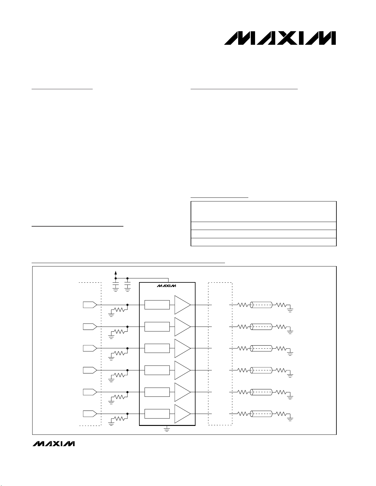
75Ω
75Ω
A/V SWITCHING
DEVICE (MAX4399)
OR BUFFERS
OUT1
IN1
+5V
0.1µF1µF
LOWPASS FILTER
WITH HF BOOST*
A = +1V/V
D/A
ENCODER
75Ω
OUT2
IN2
LOWPASS FILTER
A = +1V/V
D/A
75Ω
OUT3
IN3
LOWPASS FILTER
A = +1V/V
D/A
75Ω
OUT4
IN4
LOWPASS FILTER
A = +1V/V
D/A
75Ω
OUT5
IN5
LOWPASS FILTER
WITH HF BOOST*
A = +1V/V
D/A
75Ω
OUT6
*MAX7440 HAS FLAT RESPONSE, MAX7441/MAX7442 INCLUDES HF BOOST.
IN6
LOWPASS FILTER
WITH HF BOOST*
A = +1V/V
D/A
75Ω
75Ω
75Ω
75Ω
75Ω
MAX7440
MAX7441
MAX7442
Typical Application Circuit
STB
DVDs
Hard Disk Recorders
PVR
SCART Video Applications
General Video Filtering
PART TEMP RANGE
MAX7440ESD -40°C to +85°C 14 SO No
MAX7441ESD -40°C to +85°C 14 SO Yes
MAX7442ESD* -40°C to +85°C 14 SO Yes
PINPACKAGE
H IG H -
F R EQ U EN C Y
B O O ST

MAX7440/MAX7441/MAX7442
6-Channel Integrated Video Reconstruction
Filters
2 _______________________________________________________________________________________
ABSOLUTE MAXIMUM RATINGS
ELECTRICAL CHARACTERISTICS
(VCC= +5V ±5%, RL= 5kΩ, CL= 0 to 20pF, TA= T
MIN
to T
MAX
, unless otherwise noted. Typical values are at TA= +25°C.)
Stresses beyond those listed under “Absolute Maximum Ratings” may cause permanent damage to the device. These are stress ratings only, and functional
operation of the device at these or any other conditions beyond those indicated in the operational sections of the specifications is not implied. Exposure to
absolute maximum rating conditions for extended periods may affect device reliability.
VCCto GND ...........................................................................+6V
All Other Pins to GND.................................-0.3V to (V
CC
+ 0.3V)
Maximum Current into Any Pin .........................................±50mA
Continuous Power Dissipation (T
A
= +70°C)
14-Pin SO (derate 8.3mW/°C above +70°C)..............666.7mW
Operating Temperature Range ...........................-40°C to +85°C
Storage Temperature Range .............................-65°C to +150°C
Junction Temperature......................................................+150°C
Lead Temperature (soldering, 10s) .................................+300°C
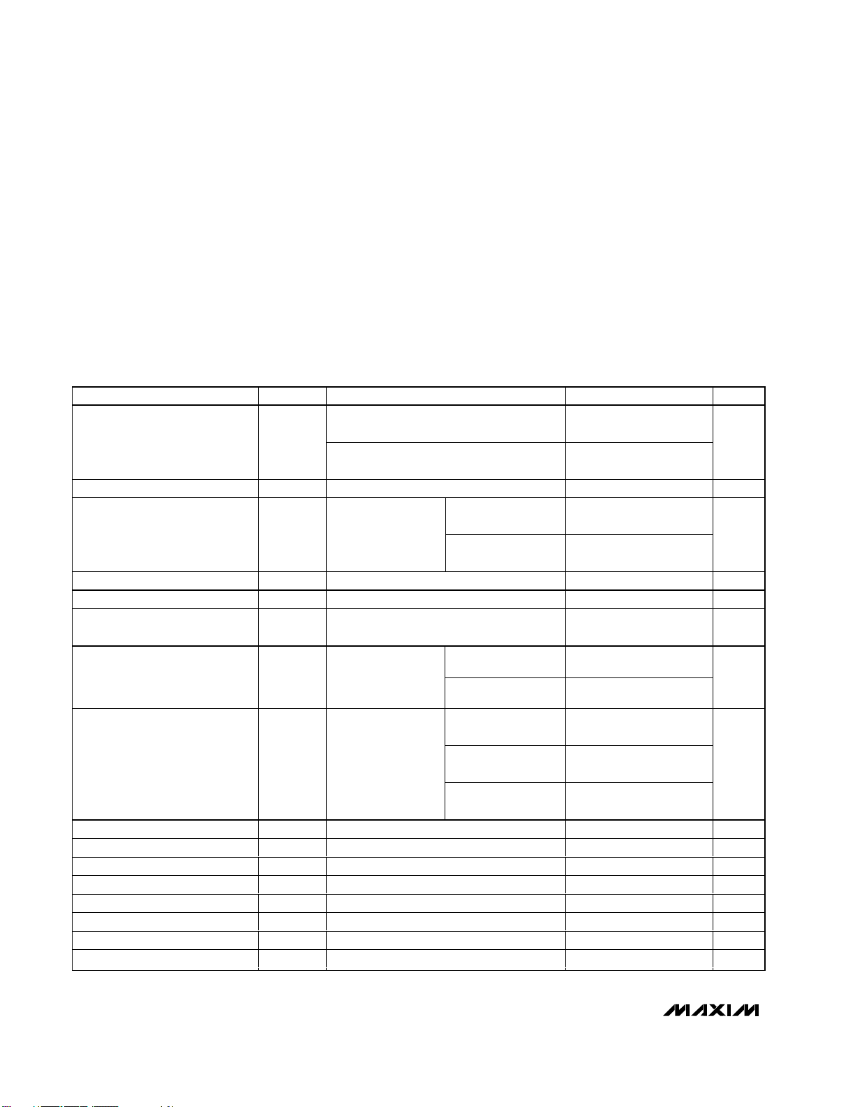
Passband Response
Stopband Attenuation A
Boost Amplitude f = 4.5MHz
Differential Gain dG 5-step modulated staircase 0.05 %
Differential Phase dB 5-step modulated staircase 0.05 Degrees
Signal-to-Noise Ratio SNR
Group Delay Matching tg(MATCH)
Group Delay Deviation ∆
Line-Time Distortion H
Field-Time Distortion V
Low-Frequency Gain Variation A
Low-Frequency Gain 0.975 V/V
Low-Frequency Gain Matching t
Input Voltage Range 0 1.75 V
Channel-to-Channel Crosstalk X
Input Leakage Current I
PARAMETER SYMBOL CONDITIONS MIN TYP MAX UNITS
sb
g
dist
dist
V
g
TALK
IN
DC to 3.5MHz, MAX7440/MAX7441
(channels 2, 3, 4)
DC to 5MHz, MAX7440/MAX7441
(channels 2, 3, 4)
f = 27MHz 37 45 dB
Peak signal (1V
to 100MHz
Low-frequency
channel-to-channel
matching,
f = 200kHz
Deviation from
100kHz to 4.5MHz
18µs, 100IRE bar -3 0 +3 mV
130 lines, 18µs, 100IRE bar -4 +4 mV
Gain at f = 100kHz -0.25 +0.25 dB
f = 100kHz -3 +3 %
Channel-to-channel crosstalk, DC to 5MHz 71 dB
VIN = 0V 2 6 25 µA
-0.40 -0.2 +0.10
-0.80 -0.5 0
+1dB HF boost,
MAX7441
+2dB HF boost,
MAX7442
) to RMS noise, f = 10Hz
P-P
Channels 2, 3, 4 2
Channels 1, 5, 6 2
MAX7440/MAX7441/
MAX7442
MAX7441 (channels
1, 5, 6)
MAX7442 (channels
1, 5, 6)
0.4 0.60 0.91
1.2
71 dB
10
17
17
dB
dB
ns
ns

MAX7440/MAX7441/MAX7442
6-Channel Integrated Video Reconstruction
Filters
_______________________________________________________________________________________ 3
ELECTRICAL CHARACTERISTICS (continued)
(VCC= +5V ±5%, RL= 5kΩ, CL= 0 to 20pF, TA= T
MIN
to T
MAX
, unless otherwise noted. Typical values are at TA= +25°C.)
0
-70
0.1 1 10 100
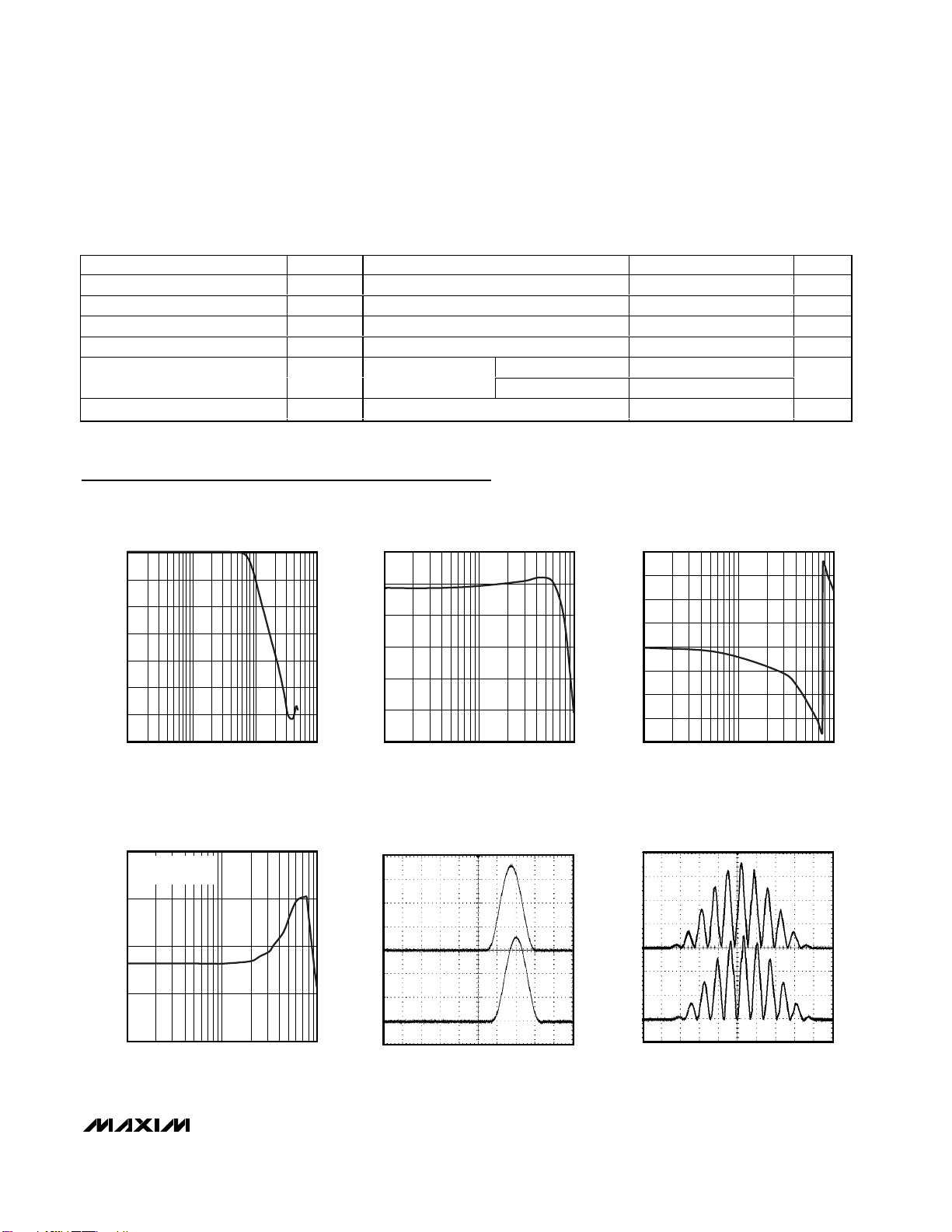
AMPLITUDE vs. FREQUENCY
-50
-60
MAX7440 toc01
FREQUENCY (MHz)
AMPLITUDE (dB)
-40
-30
-20
-10
PASSBAND AMPLITUDE vs. FREQUENCY
MAX7440 toc02
FREQUENCY (MHz)
AMPLITUDE (dB)
1
-8
-6
-4
-2
0
2
-10
0.1 10
PHASE RESPONSE vs. FREQUENCY
MAX7440 toc03
FREQUENCY (MHz)
PHASE (DEGREES)
1
-150
-100
-50
0
50
100
150
200
-200
0.1 10
80
40
0.1 1 10
GROUP DELAY vs. FREQUENCY
50
MAX7440toc04
FREQUENCY (MHz)
GROUP DELAY (ns)
60
70
MAX7441
(CHANNELS 2, 3, 4)
200ns/div
2T RESPONSE (1IRE = 7.14mV)
IN_
200mV/div
MAX7440 toc05
OUT_
200mV/div
400ns/div
MODULATED 12.5T RESPONSE
(1IRE = 7.14mV)
IN_
200mV/div
MAX7440 toc06
OUT_
200mV/div
Typical Operating Characteristics
(VCC= +5V, RL= 5kΩ, TA= +25°C, unless otherwise noted.)
PARAMETER SYMBOL CONDITIONS MIN TYP MAX UNITS
Input Resistance 200 kΩ
Input Capacitance 20 pF
Supply Voltage Range V
Supply Current I
CC
CC
Power-Supply Rejection Ratio PSRR VIN = 100mV
DC Level Shift OUT_ to IN_ 0.85 1.05 V
4.75 5.25 V
VCC = +5.5V, no load 57 78 mA
P-P
DC 39
f = 0 to 1MHz 30
dB
 Loading...