

Page 1
General Description
The MAX7428/MAX7430/MAX7432A filters are low-cost,
high-performance replacements for standard discrete filter and buffer solutions. The MAX7428/MAX7430/
MAX7432A are ideal for anti-aliasing and DAC smoothing video applications, when analog video is reconstructed from a digital data stream. These devices require a
single +5V supply and the filters have a cutoff frequency
optimized for NTSC, PAL, and standard definition digital
TV (SDTV) video signals. The MAX7428/MAX7430/
MAX7432A feature Maxim’s single-pin bus (MSPB™)
interface to digitally control channel selection (IN_A or
IN_B), adjust high-frequency boost, bypass the filter,
configure luma vs. chroma operation, and control the
output disable. The MAX7428 single-channel filter is
ideal for composite (CVBS) video signals. The MAX7430
dual filter is optimized for S-Video (Y/C) applications. The
MAX7432A triple filter is optimized for component (YPbP
r
or embedded synchronous RGB) video signals. The
MAX7428 is available in a tiny 8-pin SOT23 package, the
MAX7430 is available in a miniature 10-pin µMAX®package, and the MAX7432A is available in a 14-pin TSSOP
package. The MAX7428/MAX7430/MAX7432A are fully
specified over the -40°C to +85°C extended temperature
range.
Applications
Set-Top Boxes
DVD Players
Hard-Disk Recorders
Camcorders
Features
♦ Ideal for CVBS, Y/C (S-Video), and RGB (Y PbPr)
Outputs for NTSC, PAL, and SDTV
♦ 6th-Order Lowpass Filter
♦ Drives Two 150Ω Video Loads
♦ Four Levels of Passband High-Frequency
Boost Control
♦ Input 2 to 1 Multiplexer
♦ Output Disable
♦ Filter Bypassing
♦ +5V Single-Supply Voltage
♦ Tiny 8-Pin SOT23 Package (MAX7428), 10-Pin
µMAX Package (MAX7430), and 14-Pin TSSOP
Package (MAX7432A)
MAX7428/MAX7430/MAX7432A
Standard Definition Video Reconstruction
Filters and Buffers
________________________________________________________________ Maxim Integrated Products 1
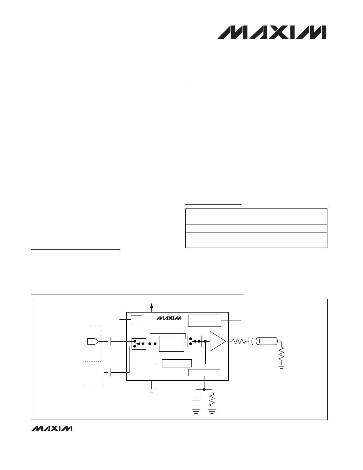
+6dB
LEVEL SHIFT
6TH-ORDER
FILTER
OUT
SERIAL INTERFACE
AND CONTROL
DATA
D/A
INA
INB
*
*OPTIONAL
SYNC
AUX INPUT
BIAS GENERATOR
GND
REXT
ENCODER
MAX7428
SYNCIO
V
CC
75Ω
75Ω
C
IN
C
IN
*
Functional Diagrams
Ordering Information
xx-xxxx; Rev 0; 2/06
Pin Configurations appear at end of data sheet.
Functional Diagrams continued at end of data sheet.
For pricing, delivery, and ordering information, please contact Maxim/Dallas Direct! at
1-888-629-4642, or visit Maxim’s website at www.maxim-ic.com.
PART
TEMP
RANGE
PIN-
TOP
MARK
MAX7428EKA-T
8 SOT23-8 AAIU
MAX7430EUB
10 µMAX —
MAX7432AEUD
14 TSSOP —
MSPB is a trademark of Maxim Integrated Products, Inc.
µMAX is a registered trademark of Maxim Integrated Products, Inc.
PACKAGE
-40°C to +85°C
-40°C to +85°C
-40°C to +85°C
Page 2
MAX7428/MAX7430/MAX7432A
Standard Definition Video Reconstruction
Filters and Buffers
2 _______________________________________________________________________________________
ABSOLUTE MAXIMUM RATINGS
ELECTRICAL CHARACTERISTICS
(VCC= +5V ±10%, R
REXT
= 300kΩ ±1%, CIN= 0.1µF, C
REXT
= (1nF to 1µF) ±1%, C
LOAD
= 0 to 20pF; BOOST0_, BOOST1_ = 0, 0;
T
A
= T
MIN
to T
MAX
, unless otherwise noted. Typical values are at TA= +25°C.) (Note 2)
Stresses beyond those listed under “Absolute Maximum Ratings” may cause permanent damage to the device. These are stress ratings only, and functional
operation of the device at these or any other conditions beyond those indicated in the operational sections of the specifications is not implied. Exposure to
absolute maximum rating conditions for extended periods may affect device reliability.
VCCto GND ...........................................................................+6V
All Other Pins to GND.................................-0.3V to (V
CC
+ 0.3V)
Maximum Current Into Any Pin .........................................
±
50mA
Continuous Power Dissipation (T
A
= +70°C)
8-Pin SOT23 (derate 9.71mW/°C above +70°C)..........777mW
10-Pin µMAX (derate 6.94mW/°C above +70°C) ......555.5mW
14-Pin TSSOP (derate 9.1mW/°C above +70°C) .........727mW
Operating Temperature Range ...........................-40°C to +85°C
Storage Temperature Range .............................-65°C to +150°C
Junction Temperature......................................................+150°C
Lead Temperature (soldering, 10s) .................................+300°C
PARAMETER
CONDITIONS
UNITS
f = 100kHz to 4.2MHz relative to 100kHz
Passband Response
f = 100kHz to 5MHz relative to 100kHz
dB
Stopband Attenuation A
sb
f
>
27MHz 48 dB
HF Boost Relative Step Size, 4
Levels
f = 4.2MHz to 5MHz 0.2 0.4 0.6 dB
Differential Gain dG 5-step modulated staircase 0.2 %
Differential Phase dθ 5-step modulated staircase 0.2
degrees
Harmonic Distortion THD f = 100kHz to 5MHz 0.1 0.5 %
Signal-to-Noise Ratio SNR
Peak signal (2Vp-p) to RMS noise,
f = 100Hz to 50MHz
72 dB
Group Delay Deviation Δt
g
Deviation from 100kHz to 3.58 (4.43)MHz 20 ns
Line-Time Distortion H
dist
18µs, 100 IRE bar 0.3 %
Field-Time Distortion V
dist
130 lines, 18µs, 100 IRE bar 0.5 %
Clamp Settling Time t
clamp
to ±1% (Note 1)
Lines
CLEVEL = 0 0.8 1.3
Output DC Clamp Level
CLEVEL = 1
V
Low-Frequency Gain A
V
Gain at 100kHz 1.9
V/V
Group Delay Matching
f = 100kHz
2ns
Low-Frequency Gain Matching
)
C hannel - to- channel g ai n m atchi ng , f = 100kH z5%
Channel-to-Channel Crosstalk X
TALK
Channel-to-channel crosstalk, f = 100kHz
to 5.5MHz
-60 dB
Output Short-Circuit Current I
SC
OUT_ shorted to ground or V
CC
50 mA
Input Leakage Current I
IN
10 µA
CLEVEL = 0 1.4
Input Dynamic Swing
CLEVEL = 1 0.9
Vp-p
VCC Supply Range V
CC
4.5 5.5 V
SYMBOL
MIN TYP MAX
-0.5 +0.5
-1.0 +1.0
t
g(MATCH)
A
V(MATCH
Y
INp-p
C
INp-p
Low frequency channel-to-channel matching
1.35 1.85
1.975 2.05
100
Page 3
MAX7428/MAX7430/MAX7432A
Standard Definition Video Reconstruction
Filters and Buffers
_______________________________________________________________________________________ 3
ELECTRICAL CHARACTERISTICS (continued)
(VCC= +5V ±10%, R
REXT
= 300kΩ ±1%, CIN= 0.1µF, C
REXT
= (1nF to 1µF) ±1%, C
LOAD
= 0 to 20pF; BOOST0_, BOOST1_ = 0, 0;
T
A
= T
MIN
to T
MAX
, unless otherwise noted. Typical values are at TA= +25°C.) (Note 2)
MSPB INTERFACE TIMING SPECIFICATIONS
(VCC= +5V ±10%, R
REXT
= 300kΩ ±1%, C
REXT
= (1nF to 1µF) ±1%, C
LOAD
= 0 to 20pF, TA= T
MIN
to T
MAX
, unless otherwise noted.
Typical values are at T
A
= +25°C.) (Figures 4 through 9)
Note 1: One horizontal line = 63.5µs.
Note 2: MAX7428 devices are 100% production tested at T
A
= +25°C and are guaranteed by design from TA= T
MIN
to T
MAX
.
PARAMETER
CONDITIONS
UNITS
MSPB TIMING
Logic-Zero/Prompt Pulse Width t0, t
P
158µs
Logic-One Pulse Width t
1
24 30 36 µs
Transaction Pulse Width t
T
80
µs
Separation Between Pulses t
WAIT
0.5 µs
Bus Release Time by Host After
Prompt Pulse
1µs
Bus Reclaim Time by Host After
Prompt Pulse
13 µs
Read Back Data Valid Window
After the Prompt Pulse
t
READ
2.3 4.7 µs
PARAMETER SYMBOL CONDITIONS MIN TYP MAX UNITS
Power-Supply Rejection Ratio PSRR V
IN_A/IN_B Crosstalk V
LOGIC CHARACTERISTICS
Logic Input High Voltage V
Logic Input Low Voltage V
Logic Input Current IIH/I
Logic Output High Voltage V
Logic Output Low Voltage V
CC
OH
OL
No load
= 100mVp-p, f = 0 to 5.5MHz 40 dB
IN
= 100mVp-p, f = 100kHz to 5.5MHz -60 dB
IN
IH
IL
VIL = 0 (source), VIH = VCC (sink) 10 µA
IL
I
(SOURCE)
I
(SINK)
= 500µA
= 500µA 0.4 V
SYMBOL
MAX7428 24 32
MAX7430 45 62Supply Current I
MAX7432A 68 86
2V
-
V
CC
0.5
MIN TYP MAX
mA
0.8 V
V
100 120
t
RELEASE
t
RECLAIM
Page 4
MAX7428/MAX7430/MAX7432A
Standard Definition Video Reconstruction
Filters and Buffers
4 _______________________________________________________________________________________
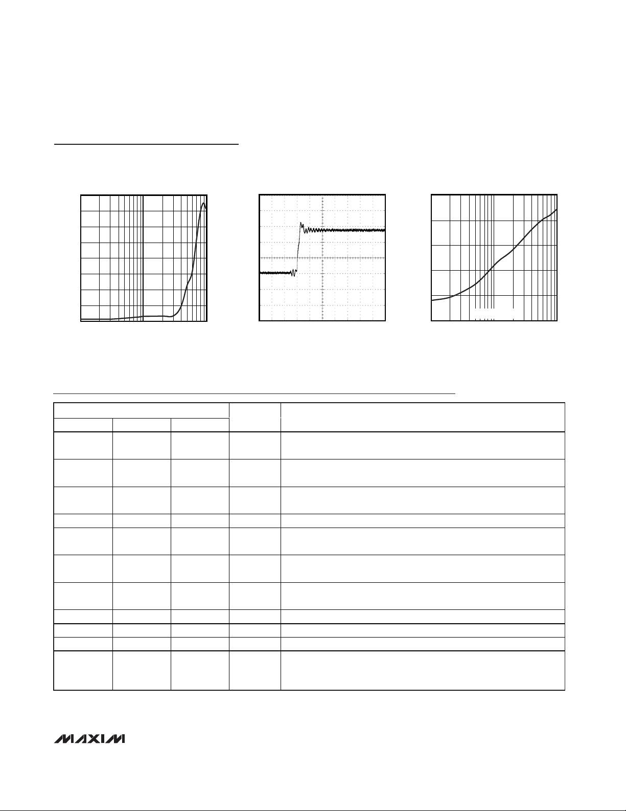
Typical Operating Characteristics
(VCC= +5V, R
REXT
= 300kΩ; BOOST0_, BOOST1_ = 0, 0; V
IN_
= 1Vp-p, TA= +25°C, unless otherwise noted.)
0.1 1 10 100
AMPLITUDE vs. FREQUENCY
MAX7428/30/32 toc01
FREQUENCY (MHz)
AMPLITUDE (dB)
0
-60
-50
-40
-30
-20
-10
0.1 1 10
PASSBAND AMPLITUDE vs. FREQUENCY
MAX7428/30/32 toc02
FREQUENCY (MHz)
AMPLITUDE (dB)
2
-10
-8
-6
-4
-2
0
A
C
D
B
A: BOOST1, BOOST0 = 1, 1
B: BOOST1, BOOST0 = 1, 0
C: BOOST1, BOOST0 = 0, 1
D: BOOST1, BOOST0 = 0, 0
0.1 1 10
PHASE RESPONSE vs. FREQUENCY
MAX7428/30/32 toc03
FREQUENCY (MHz)
PHASE (DEGREES)
180
-180
-120
-60
0
60
120
0.1 1 10
GROUP DELAY vs. FREQUENCY
MAX7428/30/32 toc04
FREQUENCY (MHz)
GROUP DELAY (ns)
120
0
20
40
60
80
100
200ns/div
2T RESPONSE (1IRE = 7.14mV)
INA_
200mV/div
OUT_
200mV/div
MAX7428/30/32 toc05
400ns/div
MODULATED 12.5T RESPONSE
(1IRE = 7.14mV)
INA_
200mV/div
OUT_
200mV/div
MAX7428/30/32 toc06
22
24
23
26
25
27
28
-40 10-15 356085
SUPPLY CURRENT vs. TEMPERATURE
MAX7428/30/32 toc07
TEMPERATURE (°C)
SUPPLY CURRENT (mA)
NO LOAD
0.2
0.1
0
-0.1
-0.2
-0.3
DIFFERENTIAL GAIN (%)
0 -0.01 -0.04 -0.08 -0.10
-0.06
1st.
2nd.
3rd. 4th.
5th.
6th.
DIFFERENTIAL GAIN
MAX7428/30/32 toc08
MAX7428/30/32 toc09
0.20
0.15
0.10
0.05
0
-0.05
1st.
2nd.
3rd.
4th.
5th. 6th.
0 0.04 0.06
0.06
0.04 0.02
DIFFERENTIAL PHASE (DEGREES)
DIFFERENTIAL PHASE
Page 5
MAX7428/MAX7430/MAX7432A
Standard Definition Video Reconstruction
Filters and Buffers
_______________________________________________________________________________________ 5
0.1 1 10
OUTPUT IMPEDANCE vs. FREQUENCY
MAX7428/30/32 toc10
FREQUENCY (MHz)
IMPEDANCE (Ω)
0
0.5
1.0
1.5
2.0
2.5
3.0
3.5
4.0
200ns/div
OUTPUT TRANSIENT DUE TO
INPUT MUX SWITCHING
OUT_
500mV/div
MAX7428/30/32 toc11
-70
-95
0.1 1 10
PASSBAND CHANNEL-TO-CHANNEL
CROSSTALK vs. FREQUENCY
-90
MAX7428/30/32 toc12
FREQUENCY (MHz)
CROSSTALK (dB)
-85
-80
-75
BOOST = CODE 00
Typical Operating Characteristics (continued)
(VCC= +5V, R
REXT
= 300kΩ; BOOST0_, BOOST1_ = 0, 0; VIN= 1Vp-p, TA= +25°C, unless otherwise noted.)
Pin Description
PIN
MAX7432A
NAME FUNCTION
1 1 — IN1A
Video Input 1A. Master channel, sync signal required. Use a 0.1µF
series input capacitor for proper operation.
2 2 — IN2A
Video Input 2A. Slave channel, clamping controlled by master channel
sync. Use a 0.1µF series input capacitor for proper operation.
3 — — IN3A
Video Input 3A. Slave channel, clamping controlled by master channel
sync. Use a 0.1µF series input capacitor for proper operation.
4, 10 8 4 GND Ground
5 4 — IN1B
Video Input 1B. Master channel, sync signal required. Use a 0.1µF
series input capacitor for proper operation.
6 5 — IN2B
Video Input 2B. Slave channel, clamping controlled by master channel
sync. Use a 0.1µF series input capacitor for proper operation.
7 — — IN3B
Video Input 3B. Slave channel, clamping controlled by master channel
sync. Use a 0.1µF series input capacitor for proper operation.
8 6 6 DATA Serial Data Interface
9 — — OUT3 Buffer Output 3
11 7 — OUT2 Buffer Output 2
12 3 7 REXT
External Resistor. Connect a 300kΩ resistor from REXT to GND for
internal biasing. Connect a 1nF to 1µF capacitor from REXT to GND for
chip-address programming (see Table 3).
MAX7430 MAX7428
Page 6
D/A
D/A
0.1μF
0.1μF
INA
INB
GND
ENCODER
75Ω
75Ω
75Ω
**220μF
75Ω
C1
300kΩ
SERIAL I/O
SYNC PULSE
IN OR OUT
OUT
V
CC
5V
REXT
DATA
SYNCIO
**220μF
*1MΩ
*1MΩ
MAX7428
Z0 = 75Ω
Z
0
= 75Ω
5V
10kΩ
***
C1 = 1nF TO 1μF (SEE TABLE 3)
*NEEDED ONLY IN FILTER BYPASS MODE
**OPTIONAL CAPACITOR
***ONLY ONE PULLUP RESISTOR NEEDED PER BUS
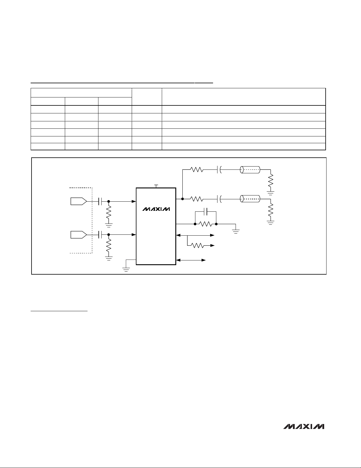
Figure 1. MAX7428 Typical Application Circuit
MAX7428/MAX7430/MAX7432A
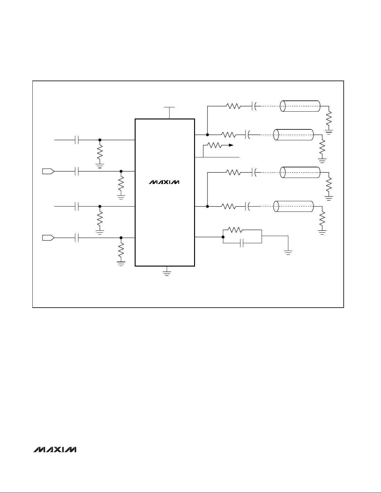
Detailed Description
The MAX7428/MAX7430/MAX7432A filter and buffer the
outputs of DAC encoder chipsets that process digital
video information in applications such as set-top boxes,
hard-disk recorders, DVD players, recorders, and digital VCRs. These devices also filter and “clean-up” analog video signals. Each channel in the MAX7428/
MAX7430/MAX7432A includes an input mux to select
the input channel, a 6th-order Sallen-Key filter with four
adjustable high-frequency boost levels, an output
buffer with a 6dB gain, a sync detector and clamp, and
an external resistor to set internal bias levels. Output
disable adds additional multiplexing in a wired-OR configuration. Filter bypass, in conjunction with the two
inputs, can be used to provide filtered and unfiltered
video signal processing. Maxim’s Single Pin Bus
(MSPB) interface controls all of the above features. An
external capacitor is used to assign each device a
unique address that allows control of up to 16 devices
on the same bus. Typical application circuits for the
MAX7428/MAX7430/MAX7432A are shown in Figures 1,
2, and 3.
Input Considerations
Use a 0.1µF ceramic capacitor to AC-couple the input
to the MAX7428/MAX7430/MAX7432A. This input
capacitor stores a DC level to level-shift the input signal
to an optimal point between VCCand GND. The ABSEL
bit on the Control Register sets which channel (IN_A or
IN_B) is selected (Control Register section). The IN_A
and IN_B inputs have a typical input resistance of
50kΩ.
Standard Definition Video Reconstruction
Filters and Buffers
6 _______________________________________________________________________________________
Pin Description (continued)
PIN
MAX7432A
NAME FUNCTION
13 9 — OUT1 Buffer Output 1
14 10 2 V
CC
+5V Supply Voltage
— — 1 INA Video Input A. Use a 0.1µF series input capacitor for proper operation.
— — 3 INB Video Input B. Use a 0.1µF series input capacitor for proper operation.
—— 5
Sync Pulse Input or Output
— — 8 OUT Buffer Output
MAX7430 MAX7428
SYNCIO
Page 7
MAX7428/MAX7430/MAX7432A
Standard Definition Video Reconstruction
Filters and Buffers
_______________________________________________________________________________________ 7
0.1μF
*1MΩ
D/A
0.1μF
*1MΩ
0.1μF
*1MΩ
D/A
0.1μF
*1MΩ
75Ω
Z
0
= 75Ω
Z
0
= 75Ω
75Ω
Z
0
= 75Ω
Z
0
= 75Ω
200μF**
200μF**
75Ω
75Ω
75Ω
75Ω
200μF**
200μF**
75Ω
75Ω
SERIAL I/O
300kΩ
C1
+5V
MAX7430
IN1A
IN1B
IN2A
IN2B
OUT1
OUT2
DATA
REXT
GND
V
CC
ENCODER
ENCODER
+5V
10kΩ
***
C1 = 1nF TO 1μF (SEE TABLE 3)
*NEEDED ONLY IN FILTER BYPASS MODE
**OPTIONAL OUTPUT CAPACITOR
***ONLY ONE PULLUP RESISTOR NEEDED PER BUS
AUX IN
AUX IN
Figure 2. MAX7430 Typical Application Circuit
Page 8

MAX7428/MAX7430/MAX7432A
Standard Definition Video Reconstruction
Filters and Buffers
8 _______________________________________________________________________________________
0.1μF
*1MΩ
D/A
0.1μF
*1MΩ
0.1μF
*1MΩ
D/A
0.1μF
*1MΩ
75Ω
75Ω
220μF**
220μF**
75Ω
75Ω
75Ω
75Ω
220μF**
220μF**
75Ω
75Ω
SERIAL I/O
300kΩ
C1
+5V
MAX7432
IN1A
IN1B
IN2A
IN2B
0.1μF
*1MΩ
D/A
0.1μF
*1MΩ
IN3A
IN3B
OUT1
OUT2
75Ω
75Ω
Z
0
= 75Ω
Z0 = 75Ω
Z0 = 75Ω
Z0 = 75Ω
Z0 = 75Ω
Z
0
= 75Ω
220μF**
220μF**
75Ω
75Ω
OUT3
DATA
REXT
GND
V
CC
ENCODER
ENCODER
ENCODER
C1 = 1nF TO 1μF (SEE TABLE 3)
*NEEDED ONLY IN FILTER BYPASS MODE
**OPTIONAL OUTPUT CAPACITOR
***ONLY ONE PULLUP RESISTOR NEEDED PER BUS
AUX IN
AUX IN
AUX IN
+5V
***
Figure 3. MAX7432A Typical Application Circuit
Page 9

MAX7428/MAX7430/MAX7432A
Standard Definition Video Reconstruction
Filters and Buffers
_______________________________________________________________________________________ 9
Filter
Filter Response
The reconstruction filter consists of a 6th-order
Butterworth filter in three second-order stages. The
Butterworth filter features a maximally flat passband for
NTSC and PAL bandwidths. The stopband offers typically 50dB of attenuation at sampling frequencies of 25MHz
and above (see Typical Operating Characteristics).
The corner frequency is not critical since the response
of the filter meets both the stopband and passband
specifications. The MAX7428/MAX7430/MAX7432A
incorporate an autotrimming feature that reduces the
corner frequency variation digitally. It is possible,
although not likely, that a discrete shift in the corner frequency may occur due to an external environmental
change. The autotrimming operates continuously so
that the corner frequency remains centered over the full
operating temperature range.
High-Frequency Boost
The high-frequency boost compensates for signal degradation and roll-off in the signal path prior to the MAX7428/
MAX7430/MAX7432A. High-frequency boost is programmable in four steps to increase image sharpness.
Output Buffer
The output buffer is able to drive two 150Ω video loads
with a 2Vp-p signal. The +6dB gain of the output buffer
is independent of the filter bypass or input selection.
The output buffer drives the 75Ω backmatch resistors
and series capacitor (typically 220µF). The MAX7428/
MAX7430/MAX7432A are able to drive the video load
directly without using the 220µF capacitor. This feature
is common in SCART applications. The OUTDISABLE bit
of the control register disables the output (mute) (see
Control Register section).
Filter Bypass
The MAX7428/MAX7430/MAX7432A offer selectable filter bypassing that allows either of the video inputs to
be filtered or unfiltered. The 1MΩ optional input resistors are needed only in filter bypass mode to provide a
discharge path for the input coupling capacitors.
Serial Interface
Maxim’s Single Pin Bus (MSPB) interface uses DATA to
transfer data to and from the microprocessor (µP) and
the MAX7428/MAX7430/MAX7432A. This negative logic
protocol uses three different pulse widths to represent
a logic “1”, logic “0”, and control commands. MSPB
allows up to 16 devices to be connected on the same
bus by assigning a unique 4-bit identification address
to each device. The µP can communicate to each
device individually or by sending a “broadcast” message to all the devices. The unique address for each
device is set by means of the time constant set by the
external capacitor connected in parallel with the external 300kΩ resistor (see Initializing the MAX7428/
MAX7430/MAX7432A section).
MAX7428 Control Register
Table 1 defines the structure of the MAX7428 8-bit control register programmed by MSPB. This register controls the selection of INA or INB, SYNCIO functionality,
filter bypassing, clamp-level selection, high-frequency
boost control, and output disable. See Maxim’s Single
Pin Bus Interface (MSPB) section for detailed programming instructions.
SYNCIO: SYNCIO Select bit. A logic 0 sets the SYNCIO
pin to function as an output while a logic 1 sets SYNCIO
to function as an input.
ABSEL: Channel Select bit. A logic 0 selects the input
at INB to be processed while a logic 1 selects the input
at INA to be processed.
BYPASS: Filter Bypass Select bit. A logic 1 selects the
filter while a logic 0 bypasses the filter.
Table 1. MAX7428 Control Register
(MSB)
FIRST BIT
(LSB)
NAME SYNCIO ABSEL BYPASS CLEVEL
—
DEFAULT 0 1 1 0 0 0 0 0
BOOST1 BOOST0
RELATIVE HIGH
FREQUENCY
BOOST
000
0 1 0.3db to 0.5db
1 0 0.6db to 1.0db
1 1 0.9db to 1.5db
Table 2. Boost Level Programming
BOOST1 BOOST0 OUTDISABLE
Page 10

MAX7428/MAX7430/MAX7432A
Standard Definition Video Reconstruction
Filters and Buffers
10 ______________________________________________________________________________________
CLEVEL: Clamp Level bit. A logic 0 selects a clamp
level of 1V while a logic 0 selects a clamp level of 1.5V
at the output.
[BOOST1, BOOST0]: High-Frequency Boost Control bits.
The adjust bits select the amount of high-frequency boost
for the filter. Table 2 defines four levels of adjustment.
OUTDISABLE: Output Disable bit. A logic 0 selects
normal operation while a logic 1 places the output in a
high-impedance state.
MAX7430 Control Register
Table 3 defines the structure of the MAX7430 16-bit control register programmed by MSPB. This register controls
the selection of IN_A or IN_B, selection of filter 1 or 2, filter
bypassing, clamp-level selection, high-frequency boost
control, and output disable. See Maxim’s Single Pin Bus
Interface (MSPB) section for detailed programming
instructions.
ABSEL_: Channel Select bit. A logic zero selects the
input at IN_B to be processed while a logic 1 selects
the input at IN_A to be processed.
BYPASS_: Filter Bypass Select bit. A logic 1 selects
the channel filter while a logic 0 bypasses the channel
filter.
CLEVEL_: Clamp Level bit. A logic 0 selects a channel
clamp level of 1V while a logic 0 selects a channel
clamp level of 1.5V at the output.
[BOOST1_, BOOST0_]: High-Frequency Boost Control
bits. The adjust bits select the amount of high-frequency
boost for the channel filter. Table 4 defines four levels of
adjustment.
OUTDISABLE_: Output Disable bit. A logic 0 selects
normal channel output operation while a logic 1 puts
the channel output in a high-impedance state.
MAX7432A Control Register
Table 5 defines the structure of the MAX7432A 24-bit
control register programmed by MSPB. This register
controls the selection of IN_A or IN_B, selection of filter
1, 2, or 3, filter bypassing, clamp-level selection, highfrequency boost control, and output disable. See
Maxim’s Single-Pin Bus Interface (MSPB) section for
detailed programming instructions.
ABSEL_: Channel Select bit. A logic zero selects the
input at IN_B to be processed while a logic 1 selects
the input at IN_A to be processed.
BYPASS_: Filter Bypass Select bit. A logic 1 selects
the channel filter while a logic 0 bypasses the channel
filter.
CLEVEL_: Clamp Level bit. A logic 0 selects a channel
clamp level of 1V while a logic 0 selects a channel
clamp level of 1.5V at the output.
[BOOST1_, BOOST0_]: High-Frequency Boost Control
bits. The adjust bits select the amount of high-frequency
boost for the channel filter. Table 6 defines four levels of
adjustment.
OUTDISABLE_: Output Disable Bit. A logic 0 selects
normal channel output operation while a logic 1 puts
the channel output in high-impedance state.
(MSB)
NAME — ABSEL2
OUT
DISABLE2
—
DEFAULT 0 1 1 0 0 0 0 0
NAME — ABSEL1
OUT
DISABLE1
—
DEFAULT 0 1 1 0 0 0 0 0
Table 3. MAX7430 Control Register
BOOST1_ BOOST0_
RELATIVE HIGH
FREQUENCY BOOST
00 0
0 1 0.3dB to 0.5dB
1 0 0.6dB to 1.0dB
1 1 0.9dB to 1.5dB
Table 4. Boost Level Programming
BYPASS2 CLEVEL2 BOOST1(2) BOOST0(2)
BYPASS1 CLEVEL1 BOOST1(1) BOOST0(1)
FIRST BIT
(LSB)
Page 11

MAX7428/MAX7430/MAX7432A
Standard Definition Video Reconstruction
Filters and Buffers
______________________________________________________________________________________ 11
Applications Information
Maxim’s Single Pin Bus (MSPB)
Serial Interface
The MSPB interface uses three pulses of different
widths to represent commands and data bits. Figure 4
shows the set of pulses that the single pin interface
uses to communicate with the device. A combination of
the one pulse (t1), zero pulse (t0), transaction pulse (tT),
and prompt pulse (tP), writes to, reads back from, and
sends broadcast data to the devices on the bus.
Note: The zero pulse and prompt pulse are the same.
Initialization pulses are significantly longer and are
used only on power-up or software reset.
Initializing the
MAX7428/MAX7430/MAX7432A
Initialization is performed only after power-up or software
reset. It assigns a unique address to each device on the
bus. The time constant of the capacitor connected to
R
EXT
in parallel with the 300kΩ resistor determines the
order in which the devices are initialized (address
assigned). The device with the largest time constant is
initialized first and so on, in descending order. Table 7
shows the “Initialize Wait” and “Initialize Time” pulse
widths needed for a specific capacitor value and tolerance. Program each device on the bus with this command sequence starting with the device with the biggest
capacitor. To reinitialize a device, cycle the power or use
a software reset. The following is the command
sequence and timing diagram (Figure 5) for initialization
as shown below. Chip ID is entered LSB first.
Note: If there is only one device on the bus, no initialization is needed. Communicate to the device using the
broadcast command described on page 13.
(MSB)
NAME — ABSEL3
OUT
DISABLE3
—
DEFAULT 0 1 1 0 0 0 0 0
NAME — ABSEL2
OUT
DISABLE2
—
DEFAULT 0 1 1 0 0 0 0 0
NAME — ABSEL1
OUT
DISABLE1
—
DEFAULT 0 1 1 0 0 0 0 0
Table 5. MAX7432A Control Register
BOOST1_ BOOST0_
RELATIVE HIGH
FREQUENCY BOOST
00 0
0 1 0.3dB to 0.5dB
1 0 0.6dB to 1.0dB
1 1 0.9dB to 1.5dB
Table 6. Boost Level Programming
ZERO/PROMPT
PULSE
t
P
= t0 = 5μs
t
1
= 30μs
t
0
ONE PULSE
TRANSACTION
PULSE
t
1
tT = 100μs
t
T
Figure 4. MSPB Interface Pulses
BYPASS3 CLEVEL3 BOOST1(3) BOOST0(3)
BYPASS2 CLEVEL2 BOOST1(2) BOOST0(2)
BYPASS1 CLEVEL1 BOOST1(1) BOOST0(1)
FIRST BIT
(LSB)
Page 12

MAX7428/MAX7430/MAX7432A
Standard Definition Video Reconstruction
Filters and Buffers
12 ______________________________________________________________________________________
Programming the
MAX7428/MAX7430/MAX7432A
An address sequence precedes a write or read operation to determine with which device to communicate. If
the address transmitted in this mode matches with a
device’s address, the device and µP can initiate data
transfer. When entering the four address bits, ensure
that the LSB is entered first. The following is the command sequence and timing diagram (Figure 6) for an
address sequence.
Use a write sequence to load data into the data register
of the device. It must follow an address sequence.
Transmit a minimum of eight data bits for the MAX7428,
16 data bits for the MAX7430, or 24 data bits for the
MAX7432A to make this transaction valid starting with
the LSB first. The last 8/16/24 data bits are used if more
than 8/16/24 bits are loaded into the register. The following is the command sequence and timing diagram
(Figure 7) for a write sequence.
During the read sequence, the µP sends a prompt
pulse causing the device to output the data word LSB
first. Similar to the write transaction, the read transaction must be preceded by an address sequence. If
more than 8 prompts (MAX7428), 16 prompts
(MAX7430), or 24 prompts (MAX7432A) are available,
the device outputs the same data starting with the LSB
again. The following is the command sequence and
timing diagram (Figure 8) for a read sequence.
Write Command Sequence:
T001
Data ≥ 8-bits (MAX7428,
See Table 1)
Data ≥ 16-bits (MAX7430,
See Table 3)
Data ≥ 24-bits (MAX7432A,
See Table 5)
T111
Table 7. Initialization Capacitor Values and Pulse Widths
(CREXT = ±10% Tolerance, RREXT = ±1% Tolerance)
Note: ( ) Indicates the time periods associated with 20% capacitors. This limits the maximum number of devices on the bus to seven.
CAPACITOR VALUE (nF)
1000 20.000 162 (136.8) 171 (144) 179 (151.2)
680 13.600 112 118 123
470 9.400 52.6 (44.1) 55.4 (46.4) 58.2 (48.72)
220 4.400 35.90 37.80 39.70
150 3.000 23.90 (13.7) 25.20 (14.4) 26.50 (15.1)
100 2.000 16.25 17.10 17.95
68 1.360 11.21 (4.4) 11.80 (4.64) 12.39 (4.9)
47 0.940 5.26 5.54 5.82
22 0.440 3.59 3.78 3.97
15 0.300 2.39 2.52 2.65
10 0.200 1.625 (1.37) 1.710 (1.44) 1.795 (1.51)
6.8 0.136 1.121 1.180 1.239
4.7 0.094 0.526 (0.441) 0.554 (0.464) 0.582 (0.487)
2.2 0.044 0.359 0.378 0.397
1.5 0.030 0.239 0.252 0.265
1 0.020 0.162 (0.137) 0.171 (0.144) 0.179 (0.151)
INITIALIZING WAIT PERIOD
(ms) (t
INTWAIT
)
INITIALIZING TIME PERIOD (ms)
WITH R
MIN TYP MAX
REXT
= 300kΩ (t
INT
)
Initialization Command Sequence:
Initialize wait T011
Initialize Time
Address ID = 4-bits T111
Address Command Sequence:
T010 Address = 4-bits T111
Page 13

MAX7428/MAX7430/MAX7432A
Standard Definition Video Reconstruction
Filters and Buffers
______________________________________________________________________________________ 13
The broadcast sequence writes data to the control registers of all the devices on the bus at the same time. Write
data with the LSB first. The following is the command
sequence and timing diagram (Figure 9) for the broadcast transaction. No address sequence is required. Use
the broadcast command when there is only one device
on the bus.
Executing a software reset serves the same function as
a power-on reset and is achieved by transmitting all
data bits (eight or more) for the MAX7428, sixteen or
more ones for the MAX7430, or 24 or more ones for the
MAX7432A to that device register.
Composite Video Filtering
The MAX7428 is ideally suited for filtering composite
video signals. Program the SYNCIO as an output when
processing composite video signals. In the rare occasion that an external sync pulse is needed to process
the composite video, program the SYNCIO as an input.
Broadcast Command Sequence:
T000
Data ≥ 8-bits (MAX7428)
Data ≥ 16-bits (MAX7430)
Data ≥ 24-bits (MAX7432A)
T111
Figure 5. Initialization Timing Diagram
ADDRESS: 0001
t
WAIT
t
T
t
T
t
1
t
1
t
0
t
1
t
1
t
1
t
0
t
0
t
0
t
0
LSB MSB
Figure 6. Address Timing Diagram
DATA: 1***000
t
WAIT
t
T
t
1
t
0
t
1
t
T
t
1
t
1
t
1
t
0
t
0
t
0
t
0
LSB MSB
Figure 7. Write Timing Diagram
Software Reset Command Sequence:
T000
8 or more 1s (MAX7428)
16 or more 1s (MAX7430)
T111
OR
T010 Address = 4-bits T111
T001
8 or more 1s (MAX7428)
16 or more 1s (MAX7430)
T111
Read Command Sequence:
Prompts ≥ 8 (MAX7428)
T101
Prompts ≥ 16 (MAX7430)
T111
Prompts ≥ 24 (MAX7432A)
t
WAIT
t
INTWAIT
t
T
t
t
0
t
1
1
t
INT
24 or more 1s (MAX7432A)
24 or more 1s (MAX7432A)
ADDRESS: 0001
t
t
1
t
0
0
t
t
T
0
t
t
1
t
1
1
LSB MSB
Page 14

MAX7428/MAX7430/MAX7432A
Standard Definition Video Reconstruction
Filters and Buffers
14 ______________________________________________________________________________________
When processing composite video set the clamp level to
+1V (CLEVEL = 0). Use the MAX7430 to process two
synchronous composite signals simultaneously. Use the
MAX7432A to process three synchronous composite
signals simultaneously.
Y/C Video Filtering
The MAX7430 is ideally suited for processing S-Video (Y/C)
signals (Figure 10). Ensure that IN1_ filters the signal that
contains the sync information (Y) since the clamping on
IN2_ is internally controlled by the master channel (IN1_)
sync. Set the clamp level for IN1_ to +1V (CLEVEL1 = 0)
and set the clamp level for IN2_ to +1.5V (CLEVEL2 = 1).
Use two MAX7428s for Y/C video filtering. Since only the
Y signal contains the sync, a typical Y/C video-filtering
application requires a master-slave configuration of the
SYNCIO. The MAX7428 processing the Y signal should
have SYNCIO configured as an output, which in turn drives the SYNCIO of the second MAX7428, processing the
C signal that has its SYNCIO configured as an input
(Figure 11). Clamping level for the Y signal should be set
for +1V (CLEVEL = 0), and clamping level for the C signal should be set for +1.5V (CLEVEL = 1). Use the
MAX7432A to filter one Y/C and one composite video
signal that are synchronous.
Component Video (RGB
or Y P
bPr
) Filtering
Component video consists of three separate signals.
Typically the three signals are separate red, green, and
blue (RGB) signals or Y (luma) and two color difference
signals: B-Y (Pb) which is blue minus luma and R-Y (Pr),
which is red minus luma. Sync information is included
with the Y signal of Y PbPrcomponent video, or in the
case of RGB, sync is usually carried on the G or on a
separate H sync line. The MAX7432A is ideally suited
for filtering component video signals. Ensure that the
sync signal (Y for Y PbPrsignals and usually G for RGB
signals) is filtered by IN1_ since IN2_ and IN3_ are
internally synced to IN1_. Set the clamp level for IN1_
to +1V (CLEVEL1 = 0) and set the clamp levels for IN2_
and IN3_ to +1.5V (CLEVEL2, 3 = 1) for Y PbPrfiltering
(Figure 12) and set all clamp levels to 1V (CLEVEL_ =
0) for RGB filtering (Figure 13). A Y PbPrcomponent
video-filter application requires three MAX7428s with
SYNCIO master-slave configuration. The MAX7428 processing the Y signal has its SYNCIO configured as an
output, which in turn drives the SYNCIO inputs of the
other MAX7428s (Figure 14). For RGB video signal filtering with a separate horizontal sync signal, configure
all MAX7428s for SYNCIO as an input (Figure 15).
t
WAIT
t
T
t
T
t
1
t
1
t
P
t
1
t
1
t
1
t
0
AB CD
HIGH-Z
t
P
t
P
READS 1ST BIT (LSB)
A: μP WILL RELEASE BUS BY TIME A
B: μP CAN START READING BIT AT TIME B
C: μP HAS UNTIL TIME C TO FINISH READING BIT
D: DEVICE WILL RELEASE BUS BY TIME D
NOTE:
TIME A, B, C, D ARE REFERENCED TO t
0
.
READS 2ND BIT REPEAT TO READ
6 MORE BITS
0 OR 1 0 OR 1
t
0
AB CD
0 OR 1
t
O
Figure 8. Read Timing Diagram
DATA: 1***000
t
WAIT
t
T
t
1
t
T
t
1
t
1
t
1
t
0
t
0
t
0
t
0
t
0
t
0
LSB MSB
Figure 9. Broadcast Timing Diagram
Page 15

MAX7428/MAX7430/MAX7432A
Standard Definition Video Reconstruction
Filters and Buffers
______________________________________________________________________________________ 15
Set the clamping levels for component video so the
MAX7428 processing Y clamps at +1V (CLEVEL = 0).
The remaining two MAX7428s should have clamp levels
set to +1.5V (CLEVEL = 1). For RGB video with external
sync (H), all three MAX7428s should have clamp levels
set to +1V (CLEVEL = 0).
Power-Supply Bypassing and Layout
The MAX7428/MAX7430/MAX7432A operate from a single +5V supply. Bypass VCCto GND with a 0.1µF
capacitor. Place all external components as close to
the devices as possible. Refer to the MAX7428EVKIT
for a proven PC board layout example.
INA
(CLEVEL = 0)
OUTY (LUMA)
SYNCIO
MAX7428
INA
(CLEVEL = 1)
OUTC (CHROMA)
SYNCIO
MAX7428
Figure 11. Y/C Video Filter Application
MAX7430
IN1A
OUT2
OUT1
IN2A
[CLEVEL = 0]
[CLEVEL = 1]
Y (LUMA)
C (CHROMA)
Figure 10. MAX7430 Y/C Video Filter Application
B
R
G
(MUST CONTAIN
SYNC SIGNAL)
MAX7432
IN1A
OUT2
OUT1
IN2A
[CLEVEL = 0]
[CLEVEL = 0]
OUT3
IN3A
[CLEVEL = 0]
Figure 13. MAX7432A RGB Video Filter with Embedded Sync
Application
P
r
P
b
Y (LUMA)
(INCLUDES
SYNC SIGNAL)
MAX7432
IN1A
OUT2
OUT1
IN2A
[CLEVEL = 0]
[CLEVEL = 1]
OUT2
IN3A
[CLEVEL = 1]
Figure 12. MAX7432A Y PbPrVideo Filter Application
Page 16

MAX7428/MAX7430/MAX7432A
Standard Definition Video Reconstruction
Filters and Buffers
16 ______________________________________________________________________________________
Chip Information
TRANSISTOR COUNT: MAX7428 = 4955
MAX7430 = 7413
MAX7432A = 9873
PROCESS: BiCMOS
INB
INA
(CLEVEL = 0)
OUTY (LUMA)
(INCLUDES
SYNC SIGNAL)
SYNCIO
MAX7428
INB
INA
(CLEVEL = 1)
OUT
P
r
SYNCIO
MAX7428
(CLEVEL = 1)
MAX7428
INB
INA
OUT
P
b
SYNCIO
Figure 14. Y PbPrVideo Filter Application
INB
INA
(CLEVEL = 0)
OUTR
SYNCIO
MAX7428
INB
INA
(CLEVEL = 0)
OUTG
SYNCIO
MAX7428
(CLEVEL = 0)
MAX7428
INB
INA
OUTB
EXTERNAL H
SYNC
SYNCIO
Figure 15. RGB Video Filter with External Sync Application
Page 17

MAX7428/MAX7430/MAX7432A
Standard Definition Video Reconstruction
Filters and Buffers
______________________________________________________________________________________ 17
DATA
SYNCIOGND
1
2
87OUT
REXTV
CC
INB
INA
SOT23
TOP VIEW
3
4
6
5
MAX7428
1
2
3
4
5
10
9
8
7
6
V
CC
OUT1
GND
OUT2IN1B
REXT
IN2A
IN1A
MAX7430
μMAX
DATAIN2B
14
13
12
11
10
9
8
1
2
3
4
5
6
7
V
CC
OUT1
REXT
OUT2GND
IN3A
IN2A
IN1A
MAX7432
GND
OUT3
DATAIN3B
IN2B
IN1B
TSSOP
Pin Configurations
SERIAL INTERFACE
AND CONTROL
BIAS GENERATOR
GND
REXT
MAX7430
V
CC
+6dB
LEVEL SHIFT
6TH-ORDER
FILTER
D/A
IN1A
IN1B
AUX INPUT
*
*
OUT1
SYNC
+6dB
LEVEL SHIFT
6TH-ORDER
FILTER
D/A
IN2A
ENCODER
*
*
OUT2
IN2B
AUX INPUT
DATA
*OPTIONAL OUTPUT CAPACITOR
Functional Diagrams (continued)
Page 18

MAX7428/MAX7430/MAX7432A
Standard Definition Video Reconstruction
Filters and Buffers
18 ______________________________________________________________________________________
Functional Diagrams (continued)
SERIAL INTERFACE
AND CONTROL
BIAS GENERATOR
GND
REXT
MAX7432
V
CC
+6dB
LEVEL SHIFT
6TH-ORDER
FILTER
D/A
IN1A
IN1B
AUX INPUT
*
*
OUT1
SYNC
+6dB
LEVEL SHIFT
6TH-ORDER
FILTER
D/A
IN2A
*
*
OUT2
IN2B
AUX INPUT
DATA
+6dB
LEVEL SHIFT
6TH-ORDER
FILTER
D/A
IN3A
ENCODER
*
*
OUT3
IN3B
AUX INPUT
*OPTIONAL OUTPUT CAPACITOR
Page 19

MAX7428/MAX7430/MAX7432A
Standard Definition Video Reconstruction
Filters and Buffers
______________________________________________________________________________________ 19
SOT23, 8L.EPS
0
0
MARKING
PACKAGE OUTLINE, SOT-23, 8L BODY
21-0078
H
1
1
Package Information
(The package drawing(s) in this data sheet may not reflect the most current specifications. For the latest package outline information,
go to www.maxim-ic.com/packages.)
Page 20

MAX7428/MAX7430/MAX7432A
Standard Definition Video Reconstruction
Filters and Buffers
20 ______________________________________________________________________________________
Package Information (continued)
(The package drawing(s) in this data sheet may not reflect the most current specifications. For the latest package outline information,
go to www.maxim-ic.com/packages.)
α
10LUMAX.EPS
α
Page 21

MAX7428/MAX7430/MAX7432A
Standard Definition Video Reconstruction
Filters and Buffers
Maxim cannot assume responsibility for use of any circuitry other than circuitry entirely embodied in a Maxim product. No circuit patent licenses are
implied. Maxim reserves the right to change the circuitry and specifications without notice at any time.
Maxim Integrated Products, 120 San Gabriel Drive, Sunnyvale, CA 94086 408-737-7600 ____________________ 21
© 2006 Maxim Integrated Products Printed USA is a registered trademark of Maxim Integrated Products, Inc.
TSSOP4.40mm.EPS
Package Information (continued)
(The package drawing(s) in this data sheet may not reflect the most current specifications. For the latest package outline information,
go to www.maxim-ic.com/packages.)
 Loading...